Semiconductor Package Types Explained: DIP, BGA, QFP, and More
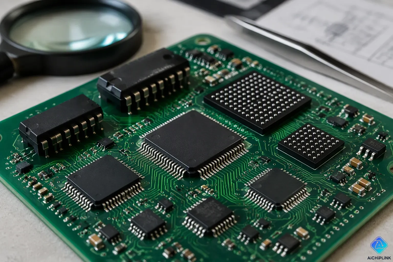
The major semiconductor package types are DIP, SOIC, QFP, QFN, BGA, CSP, WLP, SiP, and 3D packages. But first, what exactly is a semiconductor package? In short, it protects the die, connects it to the board, and manages heat and footprint.
| Source | 2024 Market Size | CAGR | 2030 Projected Size |
|---|---|---|---|
| FAQ | USD 43.95 billion | 10.2% | USD 78.72 billion |
| Market Summary | USD 39,585.2 million | 10.4% | USD 70,896.4 million |
This guide helps you compare semiconductor package options by size, pin count, thermal performance, cost, and assembly difficulty. You’ll learn about common IC package types, such as DIP packages and the BGA IC package, so you can choose the right one for your PCB design. When IC package types are explained clearly, evaluating the different types of IC packages becomes much easier. And with strong demand for advanced electronics, the semiconductor packaging market continues to grow rapidly.
Key Takeaways
-
Semiconductor packages protect the chip, connect it to the board, and manage heat.
-
Pick a package based on pin count, speed, heat, size, cost, and assembly needs.
-
DIP and PGA are through-hole packages. They are used for prototyping and for processors that go in sockets.
-
Surface-mount packages such as SOIC, QFP, and QFN take up less room and work well with machines that put parts together automatically.
-
BGA and LGA use grid arrays to fit many pins and handle heat better.
-
Modern packages such as CSP, SiP, and 3D stacking allow electronics to be smaller and faster.
-
Compare your design needs with the package comparison table to find the best match.
-
Think about how hard they are to fix: BGA and QFN are tougher to repair than DIP or QFP.
What Is a Semiconductor Package?
Definition and Core Function
A semiconductor package is a protective case around a silicon die. It holds the tiny circuit inside and connects that circuit to the printed circuit board. It also helps move heat away from the chip. Think of it as a bridge between the tiny world of transistors and the larger world of electronic devices.
The package does three main jobs. First, it protects the fragile die from moisture, dust, and physical damage. Second, it provides electrical connection through metal leads, pins, or solder bumps that carry signals to the PCB. Third, it gets rid of heat made during operation. Without a package, a bare die cannot survive real-world use.
Why Packaging Matters
Packaging shapes the performance, reliability, and cost of every electronic product. A well-designed package keeps signals clean at high speeds. It also decides how much heat the chip can release and how much board space the design uses. These factors directly affect product size, battery life, and lifespan.
The choice of package also affects manufacturing. Some packages work well with automated assembly lines. Others are better for hand soldering or prototyping. Engineers who understand integrated circuit packaging make smarter trade-offs early in a design. That knowledge saves time and money later.
Key Selection Factors
Several factors guide the choice of package. Size and footprint matter most in compact devices. Pin count must match the number of input and output signals the chip needs. Signal speed affects package choice because faster signals need shorter electrical paths. Thermal performance decides how well the package handles power without overheating. Cost and assembly difficulty complete the list, especially for high-volume production.
Different ic package types serve different needs. A simple LED driver may work fine in a dual in-line package. A high-speed processor needs a ball grid array or flip-chip design. Designers weigh these factors together. No single factor decides the outcome. The right balance depends on the application, the budget, and the manufacturing setup.
IC Package Fundamentals
Die, Substrate, and Leads
Every package starts with a die. This tiny silicon square holds the actual circuit. The die sits on a substrate, which acts as the package's foundation. The substrate provides mechanical support and sends electrical signals from the die to the outside world. Common substrate materials are laminates such as FR-4 and BT, ceramics such as alumina and aluminum nitride, and TAB materials. Some designs use ceramic, organic materials, or a blend of both.
Signals from the substrate reach the PCB through leads or bumps. Different package types use different lead frames. Ceramic packages often use alloy 42 or Invar alloy because their rate of thermal expansion matches the ceramic's. Plastic packages commonly use copper alloy lead frames, which support fine pin pitches for chip I/O redistribution. Encapsulation covers the die and protects it from moisture, dust, and physical harm. This protective shell completes the package structure.
Through-Hole vs. Surface-Mount
Packages come in three broad groups: through-hole, surface-mount, and advanced packaging. Through-hole packages use pins that go through holes in the PCB and get soldered on the far side. This method makes strong mechanical bonds. Surface-mount packages sit on the board surface. Instead of long pins, they use small leads or pads.
Surface mount technology leads modern electronics manufacturing. A Mordor Intelligence report cited by Cusack Electronics says that SMT made up 72.99% of US electronics manufacturing services process revenue in 2025. Through-hole technology is still used for power-conversion modules and avionics, but its share continues to fall. Vibration-resistant SMT packages now push into military and aerospace applications. This shift mirrors the growing demand for smaller, lighter, and faster electronic devices.
Grid Array and Advanced Approaches
Grid array packages put connections under the package body instead of around the edges. This design supports hundreds or thousands of pins in a compact area. The ball grid array uses tiny solder balls set in a grid pattern. Land grid array packages use flat pads rather than balls. These designs give shorter signal paths and better thermal performance than perimeter-lead packages.
Advanced packaging covers chip scale packages, flip-chip, multi-chip modules, system-in-package, wafer-level packaging, and 2.5D and 3D ICs. These methods stack dies vertically or put several chips side by side in one package. They save space and improve performance. Understanding IC package fundamentals helps designers compare these options. Each IC package type serves specific needs. The next sections look deeper at semiconductor packaging choices, from simple DIP packages to complex 3D stacks.
Through-Hole Packages: DIP and PGA
Through-hole packages have pins that go into drilled holes. They still show up in many designs. DIP and PGA are the main through-hole ic package types. These two ic package types make strong joints and are easy to replace.
Dual In-line Package (DIP)
Characteristics and Pin Counts
A DIP has two rows of pins that run parallel. The pins go through the PCB and are soldered on the other side. This shape makes DIP packages easy to check.
DIP pin counts stay low compared to grid array packages. Chips like op-amps and small microcontrollers use this form. The wide body limits how dense it can be.
Pros and Cons
DIP packages are cheap and good for beginners. Designers can hand-solder them or push them into sockets. Rework is simple because you can see each pin.
However, dip packages take up a lot of board space. Long pins add inductance, which hurts high-speed signals. High pin counts would make DIP too big.
Common Applications
DIP is still common in hobbyist electronics and prototyping boards. Many legacy microcontrollers still come in dip packages.
For simple circuits, DIP keeps assembly cost low. It also works well for educational kits.
Pin Grid Array (PGA)
Characteristics and Pin Counts
A PGA puts pins in a grid under the package. This layout supports far more connections than edge-lead designs. Pin counts can go over a thousand in custom sockets.
AMD specifies Socket AM4 as a 1331-opening PGA interface, indicating that AMD's AM4 platform processors still use PGA sockets.
Array positions vary by socket. Standard ZIF sockets hold up to 989 positions. Custom LIF sockets go over 1,000 positions.
Examples include FC-PGA at 370 pins for Pentium III and Celeron, PGA at 603 pins for Xeon, PPGA at 370 pins for early Celeron, and FC-PGA2 at 370/478 pins for Pentium III/Celeron and Pentium 4.
Pros and Cons
PGA gives high pin density and clean signal paths. Short pins improve electrical behavior. Socketed upgrades help desktop processors.
PGA needs careful insertion. Bent pins are easy to cause if alignment is off. Socket hardware adds cost and height.
Common Applications
PGA shows up in desktop CPUs. Intel Pentium III, Celeron, and Xeon families have used PGA packages. AMD's AM4 platform processors also use PGA sockets.
Servers and workstations rely on PGA when field replacement matters.
When Through-Hole Still Makes Sense
Through-hole packages are not obsolete. They are still useful for prototyping, education, and power circuits where mechanical strength counts. Even in an SMT-dominated world, through-hole ic package types give designers a reliable backup.
Semiconductor packaging decisions should balance density, speed, and serviceability. A DIP socket on a breadboard is still the fastest path to a working prototype. PGA suits socketed processors that need high pin counts without soldering.
Surface-Mount IC Package Types
Surface mount technology is the main way modern boards are put together. These smd ic package types sit flat on the PCB and use short leads or pads. They save space and work well with machines that do the assembly.
Small Outline Package (SOP and SOIC)
Characteristics and Pin Counts
The small outline package family makes the DIP footprint smaller so it can be surface mounted. Body width tells the variants apart. Texas Instruments and Fairchild Semiconductor draw the line this way:
Texas Instruments and Fairchild Semiconductor consistently refer to JEDEC 3.9 mm and 7.5 mm width parts as "SOIC" and to EIAJ Type II 5.3 mm width parts as "SOP".
SOIC Type Body Width Typical Pin Counts Narrow Body SOIC 3.90 mm (approx. 150 mils) 8, 14, 16 pins Wide Body SOIC 7.50 mm (approx. 300 mils) 16, 20, 24, 28 pins
The thin small outline package (TSOP) serves memory devices and is even shorter.
Pros and Cons
These packages cost little and solder easily by hand or machine. Their low profile suits dense boards. Lead inductance stays higher than grid array designs, so very fast signals suffer. Pin counts also stop well below BGA.
Common Applications
Op-amps, voltage regulators, and memory chips use this small outline package style. Automotive control modules rely on it too.
Quad Flat Package (QFP and TQFP)
Characteristics and Pin Counts
Leads come out from all four sides of a plastic quad flat pack. The thin quad flat package (TQFP) cuts height for designs with little space. A low-profile quad flat package (LQFP) offers a middle ground. Ceramic quad flat pack versions exist for harsh environments.
| Package | Lead pitch range | Pin count range |
|---|---|---|
| QFP | 0.4–1.0 mm | 32–304 pins |
| TQFP | 0.4 mm, 0.5 mm, 0.65 mm, 0.8 mm, 1.0 mm | 32–176 pins |
Pitch choices carry real meaning:
-
0.8 mm pitch: coarse pitch, easier assembly
-
0.65 mm pitch: standard industrial pitch
-
0.5 mm pitch: fine pitch, high-density designs
-
0.4 mm pitch: ultra-fine pitch, advanced applications
Pros and Cons
QFP packages handle high pin counts at moderate cost. Inspectors can see every solder joint, which helps quality control. Fine pitches demand precise placement equipment, and bent leads cause scrap.
Common Applications
Microcontrollers, DSPs, and display drivers commonly use QFP. Consumer electronics favor TQFP for its slim profile.
Quad Flat No-Lead (QFN)
Characteristics and Pin Counts
QFN packages remove the outer leads. Contacts sit flush under the body edges, and a central pad moves heat into the board. Pin counts typically range from small logic devices up to roughly a hundred contacts.
Pros and Cons
The exposed pad gives excellent thermal performance for the size. Inductance stays low, and the footprint is tiny. Solder joints hide under the package, so inspection is hard. Rework requires hot-air tools and patience.
Common Applications
QFN suits power management ICs, RF chips, and sensor hubs. Portable devices prize this smd ic package type for its small size.
Grid Array Packages: BGA and LGA
Ball Grid Array (BGA)
Characteristics and Pin Counts
A ball grid array replaces edge leads with a grid of tiny solder balls under the body. The chip connects to the board through these balls instead of pins. This layout supports very high pin counts in a small area. A bga ic package can carry hundreds of connections, and large processors use thousands.
Pros and Cons
The short path from die to ball keeps inductance low. High-speed signals travel cleanly, and heat moves into the board through the balls. The whole package stays compact for its pin count. However, solder joints hide beneath the body. X-ray inspection is often the only way to check them. Rework demands special tools and skill.
Common Applications
The bga ic package serves processors, FPGAs, and memory devices. Smartphones, laptops, and servers depend on this design. Graphics chips and network processors also use it.
Land Grid Array (LGA) and Fine-Pitch BGA
Characteristics and Pin Counts
An LGA swaps solder balls for flat pads. The socket holds the package against matching contacts on the board. Fine-pitch BGA shrinks the ball spacing and the ball size. Both designs pack many connections into a small footprint.
Pros and Cons
LGA packages sit in sockets, so users can replace them. This helps desktop CPUs and test setups. The socket adds height and cost. Fine-pitch versions need precise placement. A slight misalignment can bridge nearby pads.
Common Applications
Desktop processors often use LGA sockets. Server boards use them for easy upgrades. Fine-pitch BGA appears in mobile chips and compact modules.
Chip Scale Package (CSP)
Characteristics and Pin Counts
A chip scale package is nearly the same size as the die inside it. The IPC/JEDEC J-STD-012 definition sets the limit. The package substrate must not exceed 120% of the chip size, so the maximum package-to-die ratio is 1.2×. Ball pitch usually falls between 0.3 mm and 0.5 mm.
Pros and Cons
This is the smallest standard surface-mount category. It saves board space and shortens signal paths. The trade-offs are real. The fine pitch needs high-density interconnect boards. Rework is difficult, and inspection is limited.
Common Applications
CSP fits mobile phones, IoT devices, and RF modules. Wearables and cameras also rely on it. As semiconductor packaging advances, this form keeps shrinking.
Advanced Semiconductor Packaging
Advanced packaging goes beyond single dies in standard molded bodies. This group includes chip scale packages (CSP), flip-chip, multi-chip modules, system-in-package, wafer-level packaging, and 2.5D and 3D ICs. These methods stack dies on top of each other or place several chips side by side. They save board space, shorten signal paths, and boost performance. This semiconductor packaging class powers AI accelerators, mobile processors, and memory stacks.
Flip-Chip
Characteristics and Pin Counts
A flip-chip package attaches the die upside down. Small solder bumps connect the die to the substrate or PCB. This replaces the wire bonds of older packages. Pin counts range from dozens to thousands. The short connection path lowers inductance and delivers clean high-speed signals.
Pros and Cons
Flip-chip brings strong thermal performance because heat flows through the bumps into the board. It also makes the package smaller. The main trade-offs show up in assembly. The process needs precise placement and careful underfill to protect joints. Inspection and rework are hard once the chip sits in place.
Common Applications
High-performance computing uses flip-chip a lot. Processors, graphics chips, and network switches depend on it. The design also shows up in automotive radar and 5G transceivers.
Multi-Chip Module (MCM) and SiP
Characteristics and Pin Counts
A multi-chip module groups several bare dies on one substrate. A system-in-package (SiP) goes further and adds passive components, filters, or antennas. Pin counts change with the number of dies. Some SiPs go over a thousand external connections. These ic package types merge functions that once needed separate boxes on a board.
Pros and Cons
MCM and SiP cut total board area. They lower assembly cost by reducing the number of parts placed on the PCB. Shorter interconnects between dies improve speed and cut power loss. However, testing and known-good dies add cost. Heat from multiple dies can build up in a small space.
Common Applications
Smartphones use SiPs for power management and radio front ends. Wearables pack sensors and controllers into one module. Servers use MCMs to pair cores with cache memory.
Wafer-Level, 2.5D, and 3D Packaging
Characteristics and Pin Counts
Wafer-level semiconductor packaging builds the package right on the wafer before cutting. A wafer-level chip scale package keeps the final size almost equal to the die. Fan-out wafer-level packaging adds mold compound to create more connection area. 2.5D packaging places dies side by side on a silicon interposer. 3D packaging stacks dies vertically with through-silicon vias. Pin counts rise into the thousands for interposer designs.
Pros and Cons
Wafer-level processing cuts cost by handling many chips at once. Short paths between stacked dies reduce signal delay and power use. Stacked dies also pack the most density into the smallest footprint. Rework is nearly impossible after assembly. Thermal management becomes a challenge when multiple hot dies share one stack.
Common Applications
Mobile processors use fan-out designs to fit more I/O in less space. AI accelerators use 2.5D interposers to connect compute dies to high-bandwidth memory. Memory stacks use 3D packaging to multiply capacity.
Building Blocks of IC Packages Compared
The building blocks of ic packages decide how a chip works in a real design. Footprint, pin count, heat handling, cost, and rework difficulty all change together. The table below shows the main package families side by side.
| Package | Footprint | Pin Count | Thermal Performance | Relative Cost | Assembly Difficulty | Rework Difficulty |
|---|---|---|---|---|---|---|
| DIP | 7.6–36 mm length | 4–64 | Low | Low | Low | Low |
| SOIC | 4–18 mm length | Up to 28 | Low to moderate | Low | Low | Low |
| QFP | 7–28 mm square | Up to 256 | Moderate | Moderate | Moderate | Moderate |
| QFN | 2–12 mm square | Up to 128 | Good | Moderate | Moderate | High |
| BGA | 5–45 mm square | 2000+ | Good to high | High | High | High |
| CSP | ≤1.2× die area | Up to 400 | Moderate to good | High | High | High |
| WLP | Equal to die size | Up to 200 | Moderate | High | High | Very high |
| SiP | 3–20 mm square | Variable | Application-dependent | High | High | Very high |
| 3D/TSV | Package-level | 2000+ | High | Very high | Very high | Very high |
Footprint and Pin Count
Footprint and pin count set the first limit on any design. A 17×17 mm BGA can hold 400 or more connections. QFP cannot do that at normal pitches. That one fact explains why high-speed processors moved to grid array designs.
DIP packages range from 4 to 64 pins, and the 8-pin, 14-pin, and 16-pin types are used most. SOIC tops out near 28 pins. QFP reaches 256 pins, and QFN stops around 128. The bga ic package goes past 2000 connections. CSP and WLP stay close to die size, so their pin counts depend on the die itself. SiP pin counts change with the number of integrated dies. A 3D stack can also pass 2000 connections through through-silicon vias.
Thermal Performance and Cost
Heat removal sets the package families apart. DIP and SOIC use leads and still air, so they fit low-power parts. QFP does a bit better through its lead frame. QFN adds an exposed pad that solders right to the board, which gives strong thermal performance for its size. BGA moves heat through the solder balls into the board plane. Flip-chip and 3D stacks handle the highest power densities.
Cost follows complexity. DIP and SOIC cost the least. QFP and QFN sit in the middle. BGA, CSP, WLP, SiP, and 3D packages cost more because they need advanced substrates, fine-pitch fabrication, and tighter process control. A designer who picks a package without weighing thermal limits may face throttling or early failure. The same designer who over-specifies a package pays for capability the design never uses.
Assembly and Rework Difficulty
Assembly difficulty goes up with hidden joints. DIP and SOP are easier to probe, route, and rework. QFP holds more connections while keeping the leads visible. QFN and LGA save space and shorten connections, but their critical joints sit beneath the body. BGA and CSP raise connection density further, making footprint control, fabrication, reflow, X-ray inspection, and repair planning more demanding.
QFN inspection is a good example. QFN solder joints sit under the package and are fairly thin, so X-ray cannot reliably find open joints with too little solder. Inspection often depends on external side fillets and post-production test stations. IPC criteria for QFN side-joint defects are not yet well established.
BGA rework cost is much higher than QFP rework cost. Single short or open circuits cannot be fixed, all defects must be removed by rework, and BGA rework needs more equipment. BGA components often do not work after rework, while some QFP components can still be used if taken apart carefully. BGA rework also needs complete preheating with a smooth, gradual preheating curve. All solder balls under the BGA must be heated at the same time.
CSP rework follows a similar path with tighter tolerances. CSP solder spheres are usually about half the diameter of BGA spheres, such as 0.35 mm versus 0.55–0.75 mm. That difference calls for finer nozzle and alignment control. A dedicated placement and rework station with split vision optics, software process control, and lead-free reflow capability becomes necessary.
To read the table row by row, start with the design constraint that matters most. A tight board with low pin count points to QFN or CSP. A high pin count with moderate cost points to QFP. A high pin count with high speed points to BGA. A design that must survive field replacement points to LGA or PGA. Each row shows the trade-off the designer accepts.
Choosing the Right Package
Which semiconductor package? The answer depends on the project. The factors influencing package selection overlap in every design. Pin count, heat, speed, space, and cost all matter. No single package wins every comparison.
Pin Count and Signal Speed
Start with the number of connections. Each signal needs a pin. A simple op-amp needs eight. A modern processor can need more than five hundred. That range rules out many package families.
DIP and SOIC fit low pin counts. DIP packages usually stop near 64 pins. SOIC tops out around 28. QFP reaches roughly 256 pins. Most QFN devices sit between 12 and 64 pins. Beyond that level, the design needs a grid array. A bga ic package places solder balls under the chip. Those balls support I/O density that leaded packages cannot match. Processors and SoCs require this approach.
Signal speed matters just as much. Long leads add inductance. Through-hole packages suffer most. Surface-mount packages do better. Grid arrays shorten the path from die to board. Advanced 2.5D and 3D packaging shortens the path further. Dies sit side by side on an interposer or stack vertically. The result is lower latency. A high-speed processor with over 500 pins needs this short interconnect. Such a device also needs a package that routes on HDI or multilayer PCBs.
Thermal and Power Needs
Heat changes the package decision. A package must move heat away from the die. DIP packages rely on leads and still air. They suit low-power parts. QFP adds some metal, but not enough for high power. QFN includes an exposed pad that solders to the PCB ground plane. BGA goes further. Solder balls beneath the chip spread heat into the board. Large processors lean on this path.
Power needs set the boundary. A medium-power sensor hub runs fine in a QFN. A high-power processor needs a BGA or a 2.5D design. The 2.5D approach places dies side by side on a silicon interposer. That layout is easier to cool than a 3D stack because each die has direct access to heat paths. A 3D stack piles dies vertically, creating heat-stacking challenges. For high power, choose a package compatible with multilayer, HDI, or metalcore boards.
Manufacturing, Cost, and Rework
Manufacturing capability narrows the options. SMD ic package types such as QFN and BGA demand standard surface-mount equipment. Difficulty still changes sharply.
QFN costs less. Plastic QFN components run about $0.10 to $0.50 each. Assembly uses standard surface-mount technology. The leadless design also saves roughly 25% of board space compared with a same-size QFP. BGA costs more, between $0.50 and $2.00 per component. The ball placement process needs precise control and specialized soldering and rework equipment.
Rework difficulty follows a similar curve. QFN joints sit under the body and are hard to inspect. BGA adds X-ray inspection and full preheating. A single bad joint under a large BGA often cannot be repaired. PCB layouts should keep clearances for BGA devices at least 1 mm. Large packages need larger edge clearances, often 125 mil. Boards should avoid double-sided BGA assemblies. Placement direction matters too. Large QFP, QFN, BGA, and PoP packages should sit along the assembly-line direction. This keeps board warpage within the 0.75% solder-joint tolerance.
Now the scenarios become clear. A hobbyist building an LED driver can choose DIP or SOIC. Those packages solder easily by hand. A company making a high-volume IoT sensor should pick a QFN. It saves space and money. A team designing a high-speed processor should pick a BGA or flip-chip package. Pin count and heat leave no other option.
Common mistakes repeat across projects. Ignoring thermal limits forces a chip to run hot and throttle. Underestimating rework difficulty creates service headaches. Choosing a BGA without the right assembly equipment leads to scrap. These pitfalls separate a smooth design from a costly one. The right ic package type balances every constraint.
Different types of ic packages exist for different jobs. The right ic package type changes with the product, the line, and the budget. Semiconductor packaging choices are not universal. They are trade-offs. A designer who maps pin count, heat, and manufacturing needs early will land on a workable plan. That is the point of package selection.
Pin count, thermal performance, footprint, cost, assembly difficulty, and reworkability drive every semiconductor packaging decision. No single package wins everywhere. A dip packages choice suits a hobbyist breadboard. A ball grid array fits a high-speed processor. The right ic package type depends on your application and manufacturing context.
Use the comparison table above as a practical reference. Match your design constraints to the package families that fit.
Advanced packaging keeps evolving. Fan-out wafer-level packaging leads the market, and the overall sector should grow at roughly 10.2% yearly through 2030, exceeding US$78.72 billion. Staying informed about ic package types and semiconductor packages helps you make smarter package selection choices for future designs.

Written by Jack Elliott from AIChipLink.
AIChipLink, one of the fastest-growing global independent electronic components distributors in the world, offers millions of products from thousands of manufacturers, and many of our in-stock parts is available to ship same day.
We mainly source and distribute integrated circuit (IC) products of brands such as Broadcom, Microchip, Texas Instruments, Infineon, NXP, Analog Devices, Qualcomm, Intel, etc., which are widely used in communication & network, telecom, industrial control, new energy and automotive electronics.
Empowered by AI, Linked to the Future. Get started on AIChipLink and submit your RFQ online today!
Frequently Asked Questions
What is the difference between a package and a bare die?
A bare die is the raw silicon circuit. It has no shell and no way to connect to a board. A package adds a protective case, metal leads or bumps, and a path for heat. The package turns a fragile chip into a part that can be soldered and used.
Which package should a beginner choose for a first project?
Start with DIP or SOIC. Both solder easily by hand, and DIP works in a socket on a breadboard. Their pins stay visible, so mistakes are easy to spot. QFN and BGA hide their joints and need special tools.
Why do high-speed processors use BGA instead of QFP?
QFP tops out near 256 pins. A modern processor needs far more connections. BGA places solder balls under the body and supports over 2000 pins. The short path from die to ball also lowers inductance, which keeps fast signals clean.
Is QFN better than QFP for new designs?
It depends on the design. QFN saves roughly 25% of board space and adds an exposed pad for better heat flow. QFP keeps its leads visible, which makes inspection and rework easier. Choose QFN for size and thermal needs, QFP for serviceability.
How hard is it to rework a BGA package?
BGA rework is difficult. All solder balls must heat at the same time with a smooth preheating curve. A single bad joint under a large BGA often cannot be repaired. The part usually cannot be reused after removal.
What does chip scale package mean?
A chip scale package is nearly the same size as the die inside it. The IPC/JEDEC J-STD-012 definition caps the package at 120% of the chip size. Ball pitch usually falls between 0.3 mm and 0.5 mm.
When should a designer pick a SiP over separate chips?
Pick a SiP when board space is tight and several functions must sit close together. A SiP groups dies, passives, and sometimes antennas in one module. This shortens interconnects and cuts assembly steps. Testing and thermal buildup add cost and risk.
Do through-hole packages still have a place in modern design?
Yes. Through-hole parts give strong mechanical joints and are easy to replace. They suit prototyping, education, power circuits, and some avionics. Surface mount dominates high-volume production, but through-hole remains a reliable option for specific jobs.
How do I compare ic package types for a new board?
List your pin count, power level, board space, and assembly equipment first. Then match those needs to the comparison table above. A low pin count and hand assembly point to DIP or SOIC. High pin count and high speed point to BGA or flip-chip.