Introduction
In the realm of electronics and semiconductor technology, packaging plays a crucial role in determining the performance, durability, and cost-effectiveness of integrated circuits (ICs). One of the most widely used packaging styles in the industry is the Quad Flat Package (QFP). This package type is well-regarded for its versatility, ease of manufacturing, and efficient use in both consumer and industrial applications. Whether you are an engineer, technician, or electronics enthusiast, understanding QFP and how it compares to other packaging options is vital.
This blog will delve into the Quad Flat Package (QFP) by explaining its structure, advantages, limitations, and applications. We will also provide a comparison table for QFP versus other common package types and answer frequently asked questions (FAQs) to give you a comprehensive understanding.
What Is QFP (Quad Flat Package)?
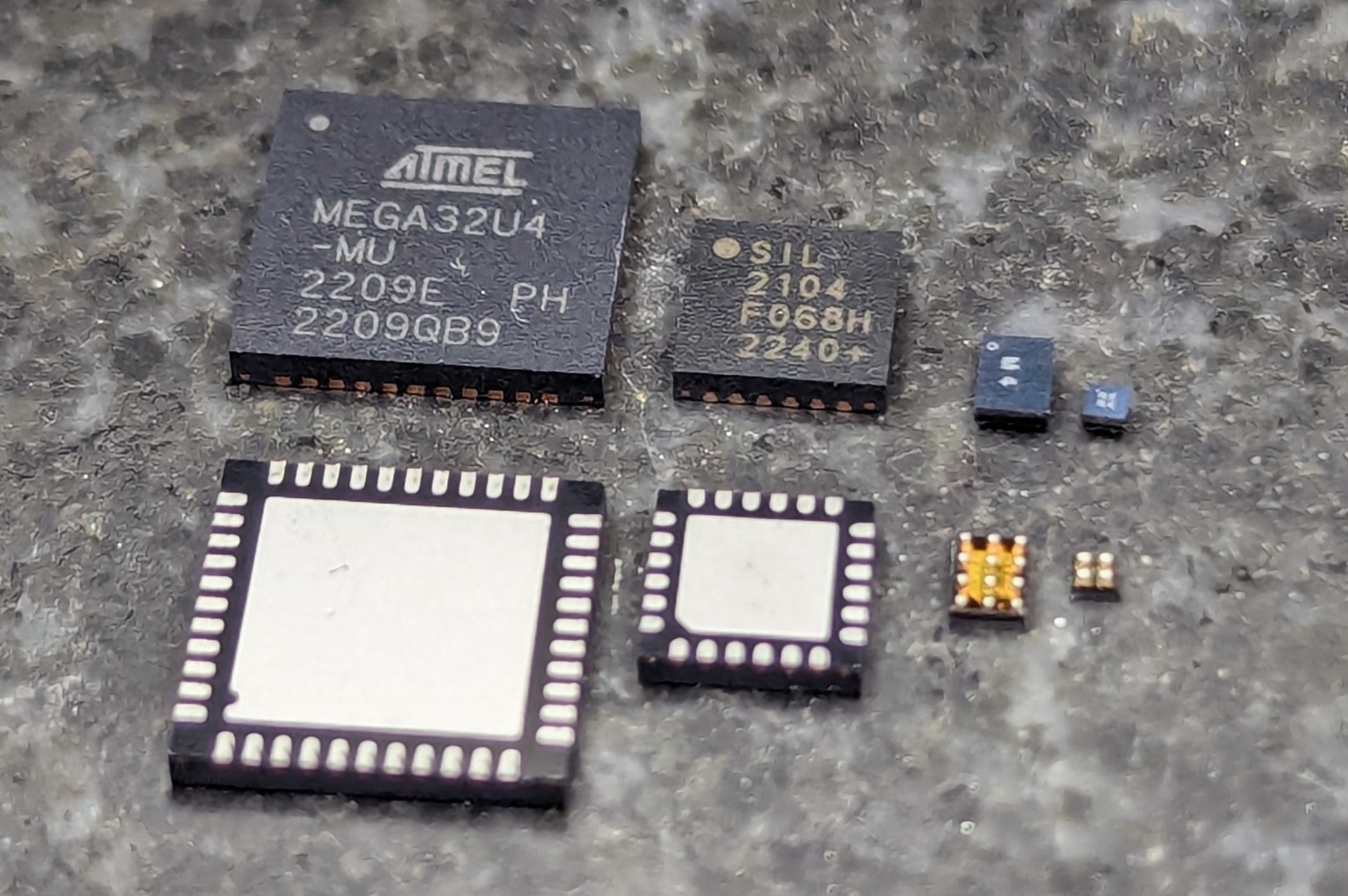
The Quad Flat Package (QFP) is a type of surface-mount packaging for integrated circuits (ICs). It features a square or rectangular form with pins (leads) extending from all four sides of the package, making it highly versatile for various electronics applications. The QFP package is designed for ease of manufacturing and efficient electrical connections, offering high-density packaging with relatively low cost and size.
Structure of QFP:
• Lead Frame: The internal structure of a QFP package consists of a lead frame that holds the semiconductor die and provides electrical connections to the leads.
• Leads: QFPs have leads on all four sides. These leads are typically arranged in a grid pattern and are used to connect the IC to a circuit board. They can be either gull-wing or J-leads.
• Body: The body of the package is made of molded plastic or other materials like ceramic. The size of the body can vary, with the most common being between 0.4 mm to 1.0 mm lead pitch (the distance between the centers of adjacent leads).
• Die Attach and Wire Bonding: The semiconductor die inside the QFP is bonded to the lead frame and connected to the leads using wire bonds or flip-chip techniques.
QFP packages are available in a wide range of sizes, from small-outline packages with few leads to large QFPs containing hundreds of leads. This adaptability makes QFP one of the most commonly used IC packages in consumer electronics, automotive systems, telecommunications, and industrial applications.
Key Features of QFP
1. Lead Count: QFP packages come in various lead counts, ranging from 16 to several hundred, which makes them suitable for different types of integrated circuits.
2. Lead Pitch: Lead pitch, the distance between adjacent leads, can vary. The most common pitch is 0.8mm, but QFP packages with 0.5mm or even 0.4mm pitch are also used for applications requiring high lead density.
3. Package Size: QFP packages are available in a variety of sizes, which allows for flexibility in design and functionality.
4. Surface Mount Technology (SMT): QFPs are designed for surface-mount technology (SMT) assembly, making them compatible with automated assembly lines for efficient production.
Advantages of QFP
• High Pin Count: One of the major advantages of QFPs is their ability to accommodate a large number of pins within a compact footprint. This makes QFP packages ideal for devices that require many I/O connections, such as microcontrollers, memory chips, and processors.
• Ease of Handling: Since QFPs are surface-mount devices (SMDs), they can be placed directly onto printed circuit boards (PCBs) during manufacturing. This reduces assembly time and minimizes the risk of defects compared to through-hole mounting.
• Low Profile: The low profile of QFPs allows for more compact circuit designs, which is especially important in industries where space is limited, such as mobile devices, consumer electronics, and automotive systems.
• Cost-Effective: Compared to other packaging technologies such as Ball Grid Arrays (BGAs), QFPs are relatively inexpensive to manufacture. This makes them a popular choice for both high-volume consumer products and less costly industrial applications.
• Thermal Performance: The design of the QFP allows for efficient heat dissipation, which is vital for maintaining optimal performance and reliability, especially in power-intensive applications.
Limitations of QFP
• Lead Pitch and Density: While QFPs can accommodate many pins, the lead pitch is limited, which can make it challenging to manufacture packages with extremely fine-pitch leads (e.g., less than 0.4mm). This may limit their use in some highly advanced applications requiring ultra-dense ICs.
• Complex Assembly: Although QFPs are easier to assemble compared to through-hole components, surface-mount assembly requires specialized equipment and techniques. For example, small-pitch QFPs require precise soldering to avoid shorts and ensure reliable connections.
• Limited Electrical Performance: QFPs are less suitable for high-speed or high-frequency applications compared to packages like BGAs, which offer better electrical performance due to shorter and more direct connections between the IC and the PCB.
• Mechanical Stress: The exposed leads of QFPs can be prone to mechanical stress, especially if the PCB is flexed or exposed to vibration. This can lead to potential issues with connection integrity over time.
QFP vs. Other Packaging Types
To better understand the benefits and limitations of QFP, it's helpful to compare it with other popular semiconductor packages. Below is a comparison table that contrasts QFP with other commonly used package types like BGA, QFN, and SOP.
| Feature | QFP | BGA | QFN | SOP |
|---|---|---|---|---|
| Lead Type | Gull-wing or J-leads | Solder balls | No leads, pads underneath | Gull-wing leads |
| Pin Count | Medium to high (16 - 500 pins) | High (100 - 1000+ pins) | Medium to high (16 - 144 pins) | Medium (8 - 48 pins) |
| Pitch | 0.4mm to 1.0mm | 0.5mm to 1.0mm | 0.5mm to 1.0mm | 0.5mm to 1.0mm |
| Package Size | Small to large | Compact, dense | Small, compact | Small to medium |
| Assembly Method | Surface-mount | Surface-mount | Surface-mount | Surface-mount |
| Cost | Relatively low | Higher cost | Low cost | Low to medium cost |
| Thermal Performance | Good | Excellent | Excellent | Moderate |
| Electrical Performance | Moderate | Excellent | Good | Moderate |
| Suitability | Consumer electronics, automotive | High-performance computing, networking | Mobile devices, low-profile applications | Low-pin count applications |
As shown in the table, QFPs are particularly well-suited for applications where a moderate to high pin count is needed, but without the requirement for extremely high-speed performance or ultra-dense packaging. BGAs and QFNs offer superior electrical performance and better thermal dissipation for high-performance applications but come at a higher cost.
Applications of QFP
QFP packages are versatile and widely used in various fields, including:
• Consumer Electronics: Microcontrollers, memory chips, and processors for smartphones, TVs, and household appliances.
• Automotive: Control units, sensor interfaces, and communication systems in cars.
• Industrial Automation: PLCs, control systems, and equipment monitoring chips.
• Telecommunications: Networking equipment, routers, and wireless communication devices.
Frequently Asked Questions (FAQs)
1. What is the difference between QFP and BGA?
The main difference between QFP and BGA lies in their lead connection style. QFP uses leads that extend from the sides of the package, while BGA uses balls of solder at the bottom. BGA packages offer better electrical performance and are more suitable for high-frequency applications, while QFPs are often preferred for lower-cost, moderate-performance applications.
2. Can QFP be used in high-speed applications?
QFP packages are not ideal for high-speed applications that require fast signal transmission. The longer lead lengths in QFP packages can introduce delays and signal degradation, making them less suitable for high-speed digital circuits compared to BGA or flip-chip packages.
3. How is a QFP package assembled onto a PCB?
QFP packages are typically assembled onto a printed circuit board using surface-mount technology (SMT). The leads are soldered onto pads on the PCB through a reflow soldering process, which ensures proper electrical connections.
4. Can I replace a QFP package with a QFN package?
QFP and QFN packages are not always interchangeable due to differences in lead configuration and physical size. While QFNs are generally smaller and more suitable for compact designs, you should ensure that the ICs' pinout, size, and thermal requirements are compatible before replacing one with the other.
5. What are the challenges of working with QFP?
Some challenges when working with QFP packages include handling fine-pitch leads, ensuring precise soldering, and managing mechanical stress during PCB
Written by Icey Ye from AIChipLink.
AIChipLink, one of the fastest-growing global independent electronic component distributors in the world, offers millions of products from thousands of manufacturers. Whether you need assistance finding the right part or electronic components manufacturers for your design, you can contact us via phone, chat or e-mail. Our support team will answer your inquiries within 24 hours.
Disclaimer: This article is provided for general information and reference purposes only. The opinions, beliefs, and viewpoints expressed by the author of this article do not necessarily reflect the opinions, beliefs, and viewpoints of AIChipLink or official policies of AIChipLink.