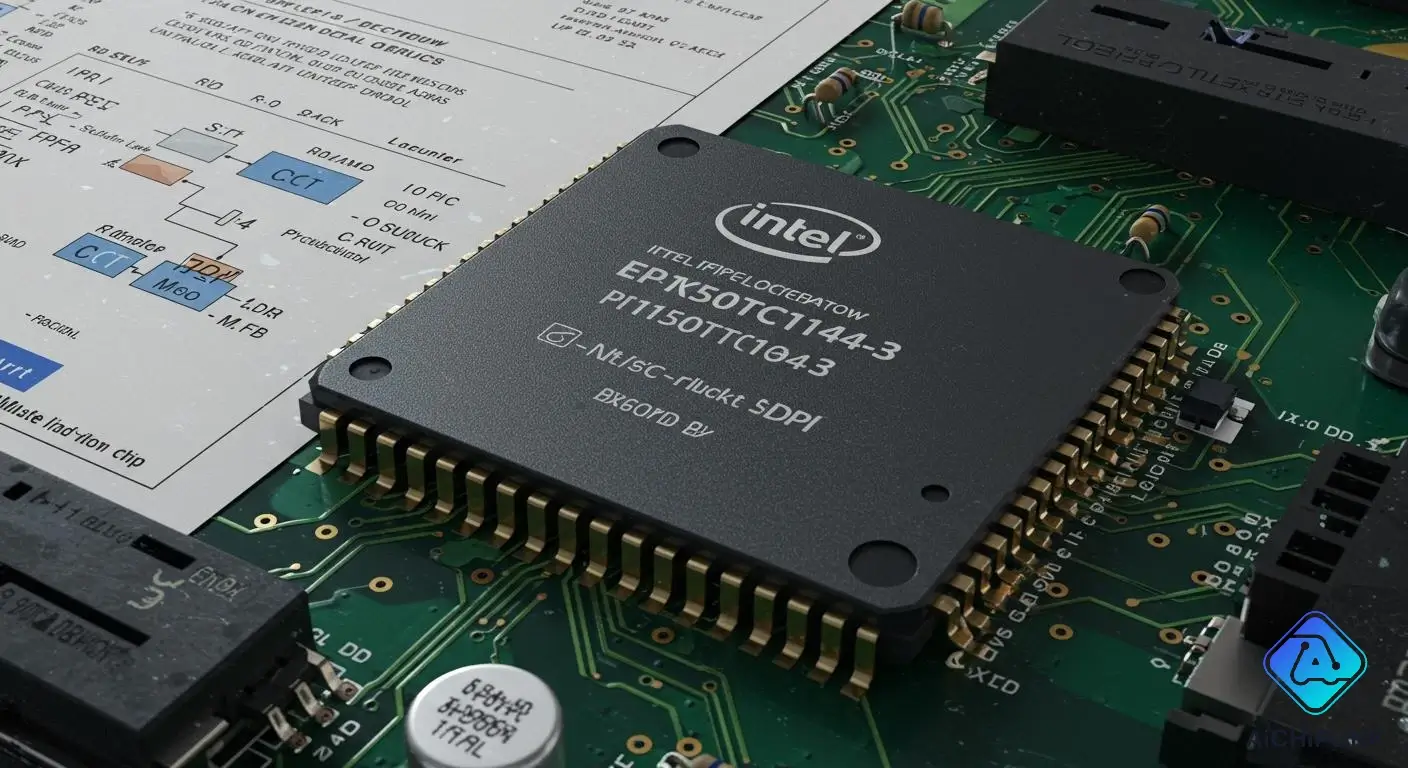
The intel fpga ep1k50tc144-3 is part of the ACEX 1K family. It is used to make digital logic designs. Engineers pick this fpga because it is fast and flexible. The list below shows its main features:
| Attribute | Value |
|---|---|
| Logic Gates | 199,000 |
| Logic Cells | 2,880 |
| Frequency | Lower than modern FPGAs |
| Voltage Supply | 2.375V ~ 2.625V |
| I/O Pins | 102 |
| Embedded Memory | 40,960 bits |
| Package Type | 144-TQFP (20x20) |
This overview shows why people should look for other options. Intel does not make this device anymore. Newer models work better.
Key Takeaways
- The Intel FPGA EP1K50TC144-3 has 2,880 logic cells and 199,000 logic gates. This makes it good for medium digital jobs. This FPGA can run at a top speed of 166.67 MHz. It can process digital signals quickly. The EP1K50TC144-3 has 102 I/O pins. This lets you connect it to many devices and circuits. The device has 40,960 bits of built-in memory. This helps it run programs and save data fast. Intel does not make the EP1K50TC144-3 anymore. You should look at newer options like Intel Cyclone IV or Xilinx Spartan-6 for better speed.
EP1K50TC144-3 Specifications
Logic Gates and Cells
The intel fpga ep1k50tc144-3 is in the acex-1k family. This fpga has thousands of logic gates and cells. These parts help it handle digital signals and do many jobs. The table below shows the main numbers for logic gates and cells:
| Number of Logic Elements/Cells | 2,880 | | Number of Gates | 199,000 |
This fpga uses 2,880 logic cells and up to 199,000 logic gates. These amounts make it good for medium digital tasks. Other acex-1k models, like EP1K30QI208-2N, have fewer gates and cells. The intel fpga ep1k50tc144-3 is a good mix of size and power.
Frequency and Technology
The fpga can run at a top speed of 166.67 MHz. This lets it finish many jobs fast. It uses 0.22-micron technology. This small size saves power and keeps it cool. The fpga has 2880 logic elements and 360 logic array blocks. These help it do many things at once. The steady voltage range also helps it use less power and work well.
Voltage and I/O Pins
The intel fpga ep1k50tc144-3 needs a voltage between 2.375V and 2.625V. This range gives it steady power and helps stop damage. The fpga has 102 input/output pins. These pins let you connect it to other parts. The table below lists the voltage and I/O pin details:
| Voltage - Supply | 2.375V ~ 2.625V | | Number of I/O | 102 |
Sometimes, the fpga can use a 3.3V supply. The many I/O pins make it useful for lots of projects.
Memory and Package
The fpga has 40,960 bits of built-in RAM. This memory saves data and helps it run programs faster. The package type is a 144-pin TQFP. The package is 20x20 mm and works safely from 0°C to 70°C. The table below shows the package details:
| Product Attribute | Attribute Value |
|---|---|
| Supplier Device Package | 144-TQFP (20x20) |
| Package / Case | 144-LQFP |
| Operating Temperature | 0°C ~ 70°C (TA) |
| Package Dimensions | 20x20 mm |
The 144-pin TQFP package makes it easy to put on boards. The memory and package help the fpga work in many digital systems.
Note: Intel does not make the intel fpga ep1k50tc144-3 anymore. You should look for other options before starting new projects. Newer fpgas work better and have more features. Always check the specs and diagram for any new device.
Intel FPGA Block Diagram
The block diagram shows how the intel fpga ep1k50tc144-3 works. It has three main parts. These are Logic Array Blocks, Embedded Memory, and I/O Structure. All parts work together to help the fpga handle signals and save data. The datasheet has a clear picture of these parts and how they connect.
Logic Array Blocks
Logic Array Blocks are in the center of the fpga. Each block has several Logic Elements inside. Logic Elements do math and logic jobs. LABs organize Logic Elements and help data move quickly. LABs use special inputs and links to connect Logic Elements. This helps the fpga do many digital jobs at once. LABs also let engineers make different circuits inside the fpga.
LABs help the fpga work faster by letting Logic Elements talk quickly. The datasheet picture shows LABs in rows and columns. They are joined by links called interconnects.
| Component | Description |
|---|---|
| Logic Array Blocks (LABs) | Made of many Logic Elements that connect for fast data movement. |
| Logic Elements (LEs) | Do math and logic jobs to make the fpga work better. |
| Interconnects | Help connect blocks so the fpga can do many digital jobs. |
Embedded Memory
Embedded Array Blocks give the fpga memory on the chip. These blocks keep data and instructions for logic jobs. EABs are next to LABs in the diagram. This makes it easy for Logic Elements to get memory fast. The fpga has 40,960 bits of memory. This memory helps run programs and save data for a short time. The datasheet picture shows EABs between LAB rows, joined by links.
-
EABs help store and get data quickly.
-
The diagram shows how EABs connect to logic blocks for good work.
I/O Structure
Input/Output Elements are around the edges of the fpga. IOEs control signals that come in and go out. The diagram shows IOEs on the outside, linking the fpga to other circuit parts. IOEs can use up to 102 I/O pins for many connections. These parts make the fpga good for lots of projects. IOEs use links to send signals to the right logic blocks or memory.
The datasheet picture shows IOEs as important for talking to other devices. IOEs help the fpga work with sensors, screens, and more.
The block diagram in the datasheet shows how LABs, EABs, and IOEs work together. The design uses rows and columns of links to join all parts. This makes data move fast and smooth. The intel fpga ep1k50tc144-3 can do hard digital jobs in many uses.
EP1K50TC144-3 Datasheet
Key Sections
The datasheet for the intel fpga ep1k50tc144-3 gives engineers important facts about the device. It helps people learn how the fpga works and how to use it in projects. The datasheet talks about a few main things:
-
Specifications: Lists main features like logic gates, logic cells, memory size, and voltage range.
-
Block Diagram: Shows a picture of the fpga inside, with logic array blocks, embedded memory, and I/O elements.
-
Memory Architecture: Tells how memory blocks work and how they link to other chip parts.
-
Pinout Information: Gives a table and pictures to show what each pin does and where it is.
-
Application Notes: Shares tips and examples for using the fpga in real circuits.
The datasheet is a full guide for anyone who wants to design with this fpga. It helps people not make mistakes and get good results.
Access and Usage
Engineers can find the datasheet on the official intel website or from trusted parts sellers. If you search for the part number, you can often get a PDF file. The datasheet usually starts with a summary table and then gives more details.
To use the datasheet well, readers should:
-
Look at the specifications table to see if the fpga is right for them.
-
Check the block diagram to learn how the main parts connect.
-
Read the pinout section before making a circuit board.
-
Go over the memory architecture and application notes for special features or tips.
A datasheet helps people plan, build, and test their designs. It gives step-by-step details for each part of the fpga. By following the datasheet, engineers can use the intel fpga ep1k50tc144-3 safely and in the best way.
Features, Applications, Alternatives
Features
The EP1K50TC144-3 has many useful features for digital design. It is part of the acex-1k family, so it uses a strong setup for medium projects. Engineers like this fpga because it is flexible. It has 102 I/O pins and 40,960 bits of embedded memory. The 144-pin TQFP package helps you put it on circuit boards easily. The specs show the fpga can go as fast as 166.67 MHz. The acex-1k series gives a clear diagram in the datasheet. This helps users see how the inside parts work.
Key Features:
-
2,880 logic cells for hard logic jobs
-
199,000 logic gates for strong power
-
102 I/O pins for lots of links
-
40,960 bits of embedded RAM
-
144-pin TQFP package for easy setup
Applications
People use the EP1K50TC144-3 in many areas. The fpga works well for signal processing, industrial control, and communication systems. Students and engineers pick acex-1k devices to learn and test ideas. The datasheet overview shows the fpga fits in test tools, motor controllers, and simple network devices. The clear diagram helps users plan their work.
Common Applications:
-
Industrial automation
-
Data collection systems
-
Motor control units
-
Learning kits
-
Communication links
Advantages and Disadvantages
The acex-1k fpga gives users some good points. It has a nice mix of logic cells and memory. The specs make it fit many jobs. The device has a simple package and a helpful diagram for easy design.
| Advantages | Disadvantages |
|---|---|
| Strong acex-1k setup | Not made by Intel now |
| Good mix of logic and memory | Slower than new FPGAs |
| Easy to put on boards | Not much support |
Users should know Intel does not make this fpga anymore. New projects might need other devices.
Alternatives
Intel stopped making the EP1K50TC144-3, so engineers should find other choices. New FPGAs have better specs and more features. Good options are Intel Cyclone IV, Xilinx Spartan-6, and Lattice ECP5. These devices are faster, have more memory, and better help.
Recommended Alternatives:
-
Intel Cyclone IV series
-
Xilinx Spartan-6 family
-
Lattice ECP5 series
Always look at the datasheet and diagram for any new fpga. Make sure it fits your project.
The EP1K50TC144-3 is a mid-level FPGA in the ACEX-1K family. It has 2,880 logic elements and 40,960 bits of built-in RAM. The 144-pin TQFP package makes it good for small designs. There are 102 I/O pins, so it works well for many tasks. People often use it in telecom, electronics, and schools.
Intel does not make this device anymore. Engineers should read datasheets closely and look at newer FPGA choices for new projects.

Written by Jack Elliott from AIChipLink.
AIChipLink, one of the fastest-growing global independent electronic components distributors in the world, offers millions of products from thousands of manufacturers, and many of our in-stock parts is available to ship same day.
We mainly source and distribute integrated circuit (IC) products of brands such as Broadcom, Microchip, Texas Instruments, Infineon, NXP, Analog Devices, Qualcomm, Intel, etc., which are widely used in communication & network, telecom, industrial control, new energy and automotive electronics.
Empowered by AI, Linked to the Future. Get started on AIChipLink.com and submit your RFQ online today!
Frequently Asked Questions
What is the main use of the EP1K50TC144-3 FPGA?
Engineers use the EP1K50TC144-3 FPGA for digital logic designs. It helps build circuits for signal processing, control systems, and learning projects. The device works well in small to medium electronic systems.
How many I/O pins does the EP1K50TC144-3 have?
The EP1K50TC144-3 provides 102 I/O pins. These pins allow the FPGA to connect with other devices, sensors, or circuits. This feature makes it flexible for many types of projects.
Can users still buy the EP1K50TC144-3 FPGA?
Intel no longer makes the EP1K50TC144-3 FPGA. Users may find leftover stock from some suppliers, but most engineers choose newer alternatives for new designs.
What package type does the EP1K50TC144-3 use?
The device uses a 144-pin TQFP package. This package measures 20x20 mm. It fits well on many circuit boards and supports easy soldering.
Where can engineers find the datasheet for the EP1K50TC144-3?
Engineers can download the datasheet from Intel’s website or trusted electronic parts distributors. The datasheet gives details about features, pinouts, and design tips.


