Introduction
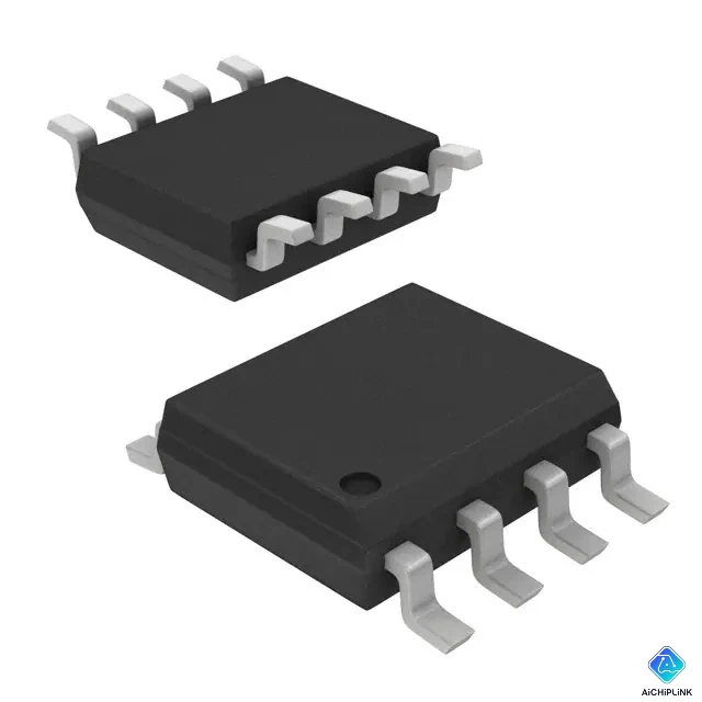
The ADG419BRZ is a precision single-pole double-throw (SPDT) analog switch manufactured by Analog Devices, featuring low on-resistance (4Ω typical), fast switching speed (85ns), and wide signal range (±15V) in SOIC-8 package, designed for signal routing, multiplexing, and precision measurement applications requiring high performance and reliability.
This CMOS analog switch provides break-before-make switching action to prevent signal short-circuits during transitions, operates from single (+5V to +36V) or dual (±5V to ±18V) supplies, and offers low leakage current (<1nA) with excellent signal integrity for audio, instrumentation, data acquisition, and automatic test equipment applications.
Technical Overview
Core Specifications
| Parameter | Specification |
|---|---|
| Configuration | SPDT (1-pole, 2-throw) |
| On-Resistance (Ron) | 4Ω typical, 7Ω max |
| Switching Time | 85ns (ton), 50ns (toff) |
| Signal Range | ±15V (dual supply) |
| Supply Voltage | 5V to 36V (single), ±5V to ±18V (dual) |
| Leakage Current | <1nA typical |
| Package | SOIC-8 |
| Operating Temp | -40°C to +85°C |
Part Number Decoder
ADG419BRZ:
- ADG = Analog Devices analog switch family
- 419 = SPDT model designation
- B = Specification grade
- R = SOIC package
- Z = Tape-and-reel packaging
Key Features
Low On-Resistance:
- 4Ω typical Ron
- Minimal signal attenuation
- Low power dissipation
- Suitable for precision applications
Fast Switching:
- 85ns turn-on time
- 50ns turn-off time
- Enables high-speed multiplexing
- Minimal signal distortion
Break-Before-Make:
- Prevents momentary shorts
- Critical for signal integrity
- Protects sensitive circuits
- Reliable switching action
Wide Supply Range:
- Single supply: +5V to +36V
- Dual supply: ±5V to ±18V
- Flexible power options
- Compatible with various systems
Complete Specifications
Switching Characteristics
| Parameter | Typical | Maximum | Unit |
|---|---|---|---|
| On-Resistance (Ron) | 4 | 7 | Ω |
| Ron Flatness | 0.5 | - | Ω |
| Ron Match | 0.2 | - | Ω |
| Turn-On Time (ton) | 85 | - | ns |
| Turn-Off Time (toff) | 50 | - | ns |
| Break-Before-Make Delay | 10 | - | ns |
Signal Specifications
| Parameter | Value |
|---|---|
| Analog Signal Range (VS = ±15V) | ±15V |
| Analog Signal Range (VS = +15V) | 0V to +15V |
| Off Leakage Current | <1nA |
| On Leakage Current | <1nA |
Digital Interface
| Parameter | Value |
|---|---|
| Logic Input High (VIH) | 2.0V min |
| Logic Input Low (VIL) | 0.8V max |
| Input Capacitance | 5pF typical |
Power Specifications
| Parameter | Typical | Maximum | Unit |
|---|---|---|---|
| Supply Voltage (Single) | - | +36V | V |
| Supply Voltage (Dual) | - | ±18V | V |
| Supply Current (IS+) | 0.01 | 0.5 | μA |
| Supply Current (IS-) | 0.01 | 0.5 | μA |
Pin Configuration
SOIC-8 Package:
Top View:

    IN    1 ●─────● 8  VDD
          │       │
    D     2 ●     │
          │       │
    VSS   3 ●     │
          │       │
    S     4 ●─────● 5  NC
          │       │
    NC    6,7 (No Connect)

Pin 1: IN (Logic control input)
Pin 2: D (Drain - common terminal)
Pin 3: VSS (Negative supply or GND)
Pin 4: S (Source - switched terminal A)
Pin 5: NC (No connect)
Pin 6: NC (No connect)
Pin 7: NC (No connect)
Pin 8: VDD (Positive supply)

Note: Actual pinout may vary - consult datasheet
Truth Table:
| IN (Logic) | Connection |
|---|---|
| LOW (0V) | D connected to S (Pin 4) |
| HIGH (VDD) | D connected to NC pin |
Application Circuits
1. Signal Routing
Audio/Signal Multiplexer:

Signal A ──► S (Pin 4)
             │
             ├── D (Pin 2) ──► Output
             │
Signal B ──► NC

Control ──► IN (Pin 1)

When IN = LOW: Output = Signal A
When IN = HIGH: Output = Signal B
Applications:
- Audio signal switching
- Sensor multiplexing
- Test point selection
- Signal path routing
2. Instrumentation Switching
Precision Measurement:

Reference ──► S
              │
              ├── D ──► ADC Input
              │
DUT Signal ─► NC

Control selects reference or DUT
Minimal Ron ensures measurement accuracy
3. Automatic Gain Control
AGC Circuit:

Input ──┬──► Gain Stage 1 ──► S
        │                     │
        └──► Gain Stage 2 ──► NC
                              │
                              ├── D ──► Output

Digital control selects gain path
Fast switching enables dynamic range adjustment
4. Bidirectional Switching
Bidirectional Communication:

Device A ◄──► D ◄──► S ◄──► Device B
                │
               IN (Control)

Break-before-make prevents bus contention
Low Ron minimizes signal degradation
Design Guidelines
Power Supply Decoupling
Single Supply (e.g., +15V):
+15V ──┬── 10μF ──┬── 0.1μF ──┬── VDD (Pin 8)
       │          │           │
      GND        GND         GND ── VSS (Pin 3)
Dual Supply (e.g., ±15V):
+15V ──┬── 10μF ──┬── 0.1μF ──┬── VDD (Pin 8)
       │          │           │
      GND        GND    Analog GND
       │                      │
-15V ──┴── 10μF ──┴── 0.1μF ──┴── VSS (Pin 3)
Signal Integrity
Minimize Ron Impact:
- Keep source impedance low
- Account for 4-7Ω in signal path
- For high-impedance sources, buffer before switch
Control Signal:
- Use CMOS/TTL logic levels
- Fast edges minimize switching time
- Pull-up/pull-down if needed for defined state
PCB Layout
Best Practices:
- Keep analog traces short
- Separate digital control from analog signals
- Ground plane under analog paths
- Bypass capacitors close to supply pins
Comparison and Selection
ADG4xx Family
| Part | Config | Ron (typ) | Supply | Speed | Use Case |
|---|---|---|---|---|---|
| ADG417 | SPST | 4Ω | ±15V | 85ns | Single switch |
| ADG419BRZ | SPDT | 4Ω | ±18V | 85ns | 2-way routing |
| ADG420 | SPDT | 25Ω | ±15V | 50ns | Lower Ron critical |
Competitive Alternatives
| Manufacturer | Part | Config | Ron | Package |
|---|---|---|---|---|
| Analog Devices | ADG419BRZ | SPDT | 4Ω | SOIC-8 |
| TI | TS5A3159 | SPDT | 0.6Ω | SOIC-8 |
| Maxim | MAX4644 | SPDT | 4Ω | SOIC-8 |
| Vishay | DG419 | SPDT | 4Ω | SOIC-8 |
ADG419BRZ Advantages:
- Proven reliability (ADI quality)
- Wide supply range
- Low leakage (<1nA)
- Break-before-make guaranteed
Conclusion
The ADG419BRZ delivers precision SPDT analog switching with low 4Ω on-resistance, fast 85ns switching, and wide ±15V signal range in reliable SOIC-8 package. With break-before-make action, low leakage (<1nA), and flexible power supply options, it enables reliable signal routing for instrumentation, audio, data acquisition, and test equipment applications.
Key Advantages:
✅ Low Ron: 4Ω typical minimizes signal loss
✅ Fast Switching: 85ns enables high-speed multiplexing
✅ Break-Before-Make: Prevents signal shorts
✅ Wide Signal Range: ±15V handles diverse signals
✅ Low Power: <0.5μA supply current
✅ Proven Quality: Analog Devices reliability
Designing precision switching systems? Visit AiChipLink.com for technical resources and analog design consultation.

Written by Jack Elliott from AIChipLink.
AIChipLink, one of the fastest-growing global independent electronic components distributors in the world, offers millions of products from thousands of manufacturers, and many of our in-stock parts is available to ship same day.
We mainly source and distribute integrated circuit (IC) products of brands such as Broadcom, Microchip, Texas Instruments, Infineon, NXP, Analog Devices, Qualcomm, Intel, etc., which are widely used in communication & network, telecom, industrial control, new energy and automotive electronics.
Empowered by AI, Linked to the Future. Get started on AIChipLink.com and submit your RFQ online today!
Frequently Asked Questions
What is ADG419BRZ used for?
ADG419BRZ is a precision SPDT analog switch commonly used for signal routing, sensor multiplexing, audio switching, and data acquisition systems where low on-resistance and fast switching are required.
What does SPDT mean in ADG419BRZ?
SPDT (Single-Pole Double-Throw) means one common pin can switch between two signal paths, allowing a circuit to select between two inputs or outputs.
What is the on-resistance of ADG419BRZ?
The device has a typical on-resistance of about 4 Ω, which helps minimize signal loss and maintain good signal integrity in precision circuits.
Can ADG419BRZ be used for audio signal switching?
Yes, it supports audio applications because it offers low on-resistance, low leakage current, and a wide signal range up to ±15 V.
What does break-before-make switching mean?
Break-before-make means the switch disconnects the current signal path before connecting to the new one, preventing short circuits or signal interference during switching.