Introduction
Generating a clean, stable negative voltage rail is one of the more deceptively challenging tasks in analog and mixed-signal PCB design. Your op-amp datasheets specify ±15 V, your ADC's reference needs −2.5 V, and your RF power amplifier bias requires −5 V — but all you have available is a 5 V or 12 V single-supply input. A charge pump can generate a rough negative rail, but it lacks current drive, regulation accuracy, and noise performance. A dedicated inverting DC-DC regulator is the right solution.
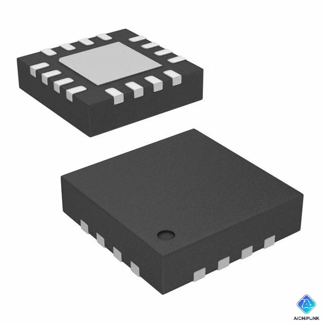
The ADP5074ACPZ from Analog Devices, Inc. is purpose-engineered for exactly this application. As a 2.4 A integrated switch, DC-to-DC inverting regulator with a 2.85 V to 15 V input range, programmable output down to VIN − 39 V, selectable 1.2 MHz / 2.4 MHz switching frequency, and a compact 3 mm × 3 mm, 16-lead LFCSP package, it is one of the most capable single-chip solutions available for generating precision negative supply rails in space-constrained designs.
According to Analog Devices' Power Management Design Center, negative rail regulators are among the most frequently misdesigned power stages in analog systems — primarily because engineers apply positive-rail regulator intuitions to a topology with fundamentally different feedback and compensation behavior. This guide will give you the theory, the formulas, and the practical layout knowledge to get it right the first time.
1.0 What Is the ADP5074ACPZ? An Overview
The ADP5074ACPZ is a high-performance, single-chip DC-to-DC inverting regulator from Analog Devices, designed to generate adjustable negative output voltages from a positive input supply. It is the highest-current member of the ADP507x inverting regulator family, integrating a 2.4 A main power switch on-chip to minimize external component count.
Decoding the part number:
- ADP — Analog Devices Power management product family
- 5074 — Specific product identifier (inverting regulator, 2.4 A switch, no boost function)
- A — Silicon revision A
- CPZ — 16-lead LFCSP (Lead Frame Chip Scale Package), 3 mm × 3 mm, exposed pad, RoHS-compliant (lead-free)
The ACPZ suffix distinguishes the commercial-grade, lead-free variant in the standard LFCSP package. The companion ordering code ADP5074ACPZ-R7 designates 7-inch tape-and-reel packaging (typically 1,500 pcs/reel), the most common procurement format.
"The ADP5074 is a high performance DC-to-DC inverting regulator used to generate negative supply rails. The integrated main switch enables the generation of an adjustable negative output voltage down to 39 V below the input voltage." — Analog Devices ADP5074 Datasheet, Rev. A
The inverting regulator topology used by the ADP5074ACPZ operates as a buck-derived inverting converter (also called a voltage-inverting or polarity-inverting topology). The output inductor, switch, and diode are arranged such that energy stored in the inductor during the on-time is released with reversed polarity during the off-time, producing a regulated negative output from a positive input rail — without a transformer.
2.0 Full Technical Specifications & Architecture
2.1 Core Electrical Parameters
Here is a complete summary from the ADP5074ACPZ datasheet (Rev. A):
- Input Voltage Range (PVIN, AVIN): 2.85 V to 15 V
- Output Voltage Range: Adjustable, down to VIN − 39 V (e.g., −36.15 V from a 2.85 V input)
- Integrated Switch Current: 2.4 A (peak, internal MOSFET)
- Switching Frequency: 1.2 MHz (SYNC/FREQ pin = GND) or 2.4 MHz (SYNC/FREQ pin = VREG)
- External Sync Frequency Range: 1.0 MHz to 2.6 MHz
- Reference Voltage (VREF): 1.60 V ±0.5% (25°C); ±1.5% (−40°C to +125°C)
- Feedback Voltage (VREF − VFB): 0.8 V ±0.5% (25°C)
- Feedback Bias Current (IFB): 0.1 µA (typical)
- Load Regulation: 0.0006 %/A (20 mA to 1500 mA, non-skip mode)
- Operating Quiescent Current (IQ): 1.8 mA typical / 4.0 mA maximum (EN = high, no switching)
- Shutdown Current (ISHDN): 5 µA typical / 10 µA maximum (EN = low)
- UVLO Rising Threshold: 2.85 V; Falling: 2.55 V; Hysteresis: 0.25 V
- Precision Enable High Threshold (VTH_H): 1.15 V typical
- Precision Enable Low Threshold (VTH_L): 1.05 V typical
- Internal VREG Output: 4.25 V (powers internal gate drive)
- Junction Temperature Range: −40°C to +125°C
- Package: 16-lead LFCSP, 3 mm × 3 mm body, 0.5 mm pitch, exposed pad (EP)
- RoHS Compliant: Yes (Z suffix, lead-free matte tin termination)
- ESD Rating: ±2 kV (HBM, per ANSI/ESDA/JEDEC JS-001)
The ±0.5% reference voltage accuracy at 25°C is exceptional for a switching regulator — comparable to precision LDO references — and reflects ADI's analog design heritage. In a negative rail for a 16-bit ADC, this accuracy directly translates to reference voltage error at the converter input.
2.2 Switching Frequency, SYNC, and UVLO
The ADP5074ACPZ offers a pin-selectable dual switching frequency: tie SYNC/FREQ to GND for 1.2 MHz, or tie to VREG (4.25 V internal supply) for 2.4 MHz. Alternatively, an external clock from 1.0 MHz to 2.6 MHz can be injected on the SYNC/FREQ pin to synchronize the regulator to a system master clock — a critical feature in noise-sensitive analog and RF applications where asynchronous switching intermodulation must be avoided.
When to choose 1.2 MHz vs. 2.4 MHz:
- 1.2 MHz: Allows use of a larger inductor (lower peak current, lower core losses), achieves slightly higher efficiency at full load, and is preferred for applications where inductor size is not a constraint.
- 2.4 MHz: Enables smaller passives (inductor, input/output capacitors), reduces solution footprint, and is preferred in space-constrained PCBs. The higher frequency also pushes switching harmonics above the most sensitive audio and measurement frequency bands (> 2 MHz).
The precision UVLO (Undervoltage Lockout) at 2.85 V rising / 2.55 V falling prevents the regulator from operating in dropout — a condition that would cause the output to become unregulated and potentially damage downstream load circuits. The 0.25 V hysteresis prevents chattering during slow input ramps.
2.3 Protection Features: OCP, OVP, TSD, and Power Good
The ADP5074ACPZ implements a comprehensive protection suite:
- Overcurrent Protection (OCP): Cycle-by-cycle current limiting on the integrated 2.4 A switch. When switch current exceeds the threshold, the current cycle is terminated immediately, preventing inductor saturation and switch damage.
- Overvoltage Protection (OVP): Monitors the FB pin voltage relative to VREF. If the output voltage becomes excessively negative (OVP threshold: 0.74 V at FB pin, triggered when output swings too far negative), the regulator halts switching until the condition clears.
- Thermal Shutdown (TSD): The device shuts down automatically if junction temperature exceeds approximately 165°C and resumes operation after the die cools, providing self-protection without requiring external thermal monitoring.
- Undervoltage Lockout (UVLO): Described above — prevents operation below safe input voltage thresholds.
- Power Good (PWRGD): An open-drain output that pulls low when the regulated output is within spec (FB voltage within window of VREF). The PWRGD pin can drive an LED, a logic enable signal, or a power sequencing controller — an invaluable feature in multi-rail systems where rail sequencing order matters.
- True Shutdown: When EN is pulled below the shutdown threshold (< 0.4 V), the ADP5074ACPZ completely disconnects the load from the input supply — not just stops switching, but achieves genuine high-impedance output isolation. This prevents back-feeding and allows proper sequencing in multi-supply systems.
3.0 Negative Rail Application Design
3.1 Bipolar Op-Amp, ADC, and DAC Supply Rails
The single most common application for the ADP5074ACPZ is generating the negative supply rail for precision analog circuits: bipolar op-amps, instrumentation amplifiers, precision ADCs, high-speed DACs, and analog multiplexers. These circuits require:
- A stable, low-noise negative supply — any noise on the negative rail couples directly into signal chains
- Accurate output voltage — op-amp input offset and ADC reference error are both sensitive to supply voltage deviation
- Sufficient current capacity — a PCB with 4–8 op-amps, one 16-bit ADC, and a DAC may draw 200–600 mA from the negative rail
A typical design example: generating −12 V at up to 500 mA from a 5 V system bus for a precision instrumentation front-end.
Output voltage setting formula:
The output voltage is set by the external resistor divider (RFT, RFB) from the output node to the FB pin:
VOUT = −VREF × (1 + RFT / RFB) − VREF_FB × RFT / RFB
Simplified for practical use (VREF = 1.60 V, VREF−VFB = 0.8 V):
|VOUT| ≈ 0.8 × (1 + RFT / RFB)
For example, to generate −12 V output: RFT / RFB = (12 / 0.8) − 1 = 14. With RFB = 10 kΩ, RFT = 140 kΩ (use 137 kΩ standard value for closest match).
Noise reduction strategies for analog applications:
- Place a 10 µF + 100 nF ceramic capacitor directly at the output to filter switching ripple
- Add a small RC post-filter (10 Ω + 10 µF) between the switching regulator output and sensitive analog supply pins for an additional 20–40 dB of high-frequency noise rejection
- Synchronize ADP5074ACPZ to the ADC sampling clock or an exact sub-multiple thereof to prevent beat-frequency interference in the signal band
- Use the 2.4 MHz frequency option to push switching harmonics above the measurement bandwidth of most precision signal chains
3.2 RF PA Bias and Optical Module Power
RF power amplifiers — particularly GaAs pHEMT and GaN devices — require accurate, stable negative gate bias voltages (typically −0.5 V to −5 V) to set the quiescent operating point. The ADP5074ACPZ is well-suited for this role:
- Its precision enable pin (1.15 V threshold) allows the gate bias rail to be sequenced precisely relative to the drain supply, preventing gate-drain breakdown during power-up
- The programmable soft start prevents inrush current spikes that could damage sensitive PA devices at power-on
- The 2.4 MHz switching option keeps switching harmonics well above typical RF signal bands (< 6 GHz applications with 2.4 MHz harmonic well above the signal channel)
- The true shutdown feature completely removes the negative gate bias during power-down, ensuring the PA is safely pinched off before drain power is removed
In optical transceiver modules (SFP, QSFP, CFP), the ADP5074ACPZ generates the −5.2 V and −3.3 V supplies for the laser driver and TIA (transimpedance amplifier) circuitry, where the tight 3 mm × 3 mm footprint and high switching frequency (small passives) are critical for meeting optical module mechanical form factors.
3.3 Skip Mode and Light-Load Efficiency
At light loads (typically below 10–15% of rated output current), the ADP5074ACPZ automatically transitions into skip mode — a pulse-skipping operation that maintains output voltage regulation by delivering energy pulses only when the output capacitor voltage drops below the regulation threshold, then skipping switching cycles when energy is not needed.
Skip mode dramatically improves light-load efficiency by eliminating the fixed switching losses (gate drive, core loss, diode conduction) during intervals when the load draws minimal current. This is particularly valuable in:
- Battery-powered systems where standby current determines battery life
- IoT sensor nodes that spend most of their time in low-power sleep, with the negative rail powering an op-amp in a low-current measurement mode
- Always-on monitoring circuits where the negative rail powers a comparator or reference circuit drawing only a few milliamps
The transition between PWM mode and skip mode is seamless and automatic — no external control logic is required. The quiescent current in skip mode (excluding switching losses) is dominated by the 1.8 mA typical IQ, which sets a floor on idle power consumption.
The video above covers inverting regulator topology fundamentals, ADP507x family selection, output voltage programming, and compensation design using the ADIsimPower design tool.
4.0 ADP5074ACPZ vs. Competing Inverting Regulators
4.1 ADP5074 vs. ADP5073, ADP5071, and ADP5075
| Feature | ADP5074ACPZ | ADP5073ACPZ | ADP5071ACPZ | ADP5075 (WLCSP) |
|---|---|---|---|---|
| Inverter Switch Current | 2.4 A | 1.2 A | 1.2 A | 0.8 A |
| Boost Switch Current | None | None | 2.0 A | None |
| Input Voltage Range | 2.85 V – 15 V | 2.85 V – 15 V | 2.85 V – 15 V | 2.85 V – 15 V |
| Switching Frequency | 1.2 / 2.4 MHz | 1.2 / 2.4 MHz | 1.2 / 2.4 MHz | 1.2 / 2.4 MHz |
| Soft Start | Programmable | Fixed internal | Programmable | Fixed internal |
| Slew Rate Control | Yes | No | Yes | No |
| SYNC Input | Yes | Yes | Yes | Yes |
| Package | 16-LFCSP (3×3 mm) | 16-LFCSP (3×3 mm) | 20-LFCSP (4×4 mm) | 12-ball WLCSP (1.61×2.18 mm) |
| Power Good (PWRGD) | Yes | Yes | Yes | No |
Key decision guide within the ADP507x family:
- Need 2.4 A inverter only → ADP5074ACPZ (this device — highest inverter current in compact 3×3 mm package)
- Need 1.2 A inverter only, smaller BOM → ADP5073ACPZ (same package, lower switch current, no slew control)
- Need both boost + inverter from one IC → ADP5071ACPZ (generates both positive boost and negative inverter outputs simultaneously — ideal for bipolar ±15 V from a 5 V rail using a single IC)
- Ultra-miniature WLCSP required → ADP5075 (1.61 × 2.18 mm, only 0.8 A, no PWRGD — for wearables and very small form factors)
Versus competing vendors:
Compared to Texas Instruments' TPS63700 (60 mA — much lower current, different application niche) and Maxim's MAX1760 (similar inverter concept, older process node, larger package), the ADP5074ACPZ offers the best combination of switch current, frequency agility, protection features, and package density in its class.
4.2 Pricing, Availability & Evaluation Tools
The ADP5074ACPZ-R7 (7-inch reel, standard ordering format) is an active production part with broad global availability:
- Authorized distributors: DigiKey, Mouser, Arrow, Avnet, Future Electronics
- Typical unit pricing: ~$2.50–$4.50 USD (1k+ quantity, varies by distributor and market conditions)
- Evaluation board: ADP5074CP-EVALZ — pre-populated demonstration board covering line/load regulation, efficiency measurement, and frequency synchronization testing; orderable from Analog Devices directly
- Design tool: ADIsimPower — Analog Devices' free online design tool generates complete schematics, BOM, component values, and performance predictions for the ADP5074ACPZ with user-defined VIN, VOUT, IOUT, and frequency inputs
- RoHS status: Fully compliant (Z suffix, matte tin termination)
- ECCN: EAR99
For competitive pricing, verified authentic Analog Devices inventory, and volume RFQ support, visit aichiplink.com — ADP5074ACPZ listing.
5.0 PCB Layout, Loop Compensation & Design Guidelines
5.1 LFCSP Layout and Critical Routing Rules
The 16-lead LFCSP (3 mm × 3 mm) package has a central exposed pad (EP) that must be soldered to the PCB ground plane for both electrical and thermal conduction. Follow these layout priorities:
- Exposed pad (EP) thermal vias: Place a grid of at least 4–9 thermal vias (0.3 mm drill, filled or tented) under the EP, connecting to the inner ground plane. This is essential for thermal management — without EP soldering, the thermal resistance increases by 3–5× and the device will throttle via TSD at modest loads.
- SW node copper area: The SW pin connects to the switching node (inductor, diode junction). Keep this copper area as small as possible — it is the primary EMI radiator. Route the inductor and diode directly to the SW pin with short, direct traces. Do not use a large copper pour on the SW node.
- Inductor placement: Place the inductor immediately adjacent to the SW pin, with the far terminal of the inductor connecting to the output capacitor and diode return node. Minimize the high-current switching loop area: SW pin → inductor → output capacitor → diode → PVIN decoupling capacitor → SW pin.
- Input capacitor (CIN): Place the PVIN decoupling capacitor (10 µF + 100 nF) as close as possible to the PVIN pin, with the return path directly to GND via a short low-inductance route.
- Output capacitor (COUT): Place directly at the output node, with the negative terminal of COUT on the GND plane (note: in an inverting regulator, the "output" is negative — the polarity is inverted relative to a standard buck).
- VREG and VREF bypass capacitors: Place 1 µF capacitors directly at the VREG and VREF pins — these internal supply pins are sensitive to layout parasitic inductance.
- COMP network: The compensation RC network (from COMP pin to GND) should be placed within 5 mm of the COMP pin.
- Feedback resistors (RFT, RFB): Route the FB node with a short, shielded trace away from the SW node to avoid noise coupling into the error amplifier. Keep RFT and RFB physically close to the FB pin.
5.2 Output Voltage Setting and Feedback Resistors
The output voltage is set by the ratio of two external resistors connected between VOUT, FB, and GND:
|VOUT| = 0.8 × (1 + RFT / RFB)
Recommended design procedure:
- Choose RFB = 10 kΩ (low enough to overcome IFB = 0.1 µA bias current error, high enough to limit quiescent divider current)
- Calculate RFT = RFB × (|VOUT| / 0.8 − 1)
- Select nearest standard E96 resistor value for RFT
- Verify actual VOUT with the standard value: VOUT_actual = −0.8 × (1 + RFT_actual / 10k)
Common output voltage settings:
| Target VOUT | RFB | RFT (calculated) | RFT (E96 standard) | Actual VOUT |
|---|---|---|---|---|
| −3.3 V | 10 kΩ | 31.25 kΩ | 31.6 kΩ | −3.328 V |
| −5.0 V | 10 kΩ | 51.5 kΩ | 51.1 kΩ | −4.888 V |
| −12.0 V | 10 kΩ | 140 kΩ | 137 kΩ | −11.76 V |
| −15.0 V | 10 kΩ | 176.25 kΩ | 174 kΩ | −14.72 V |
Use the ADIsimPower design tool (free at analog.com) to automate component selection, verify stability margins, and generate a complete BOM including inductor, diode, and capacitor values for your specific VIN, VOUT, and IOUT requirements.
5.3 Soft Start, Slew Rate Control, and Loop Compensation
Soft start (SS pin): Connecting a resistor (RSS) from the SS pin to GND sets the soft start time. Leaving the SS pin open selects the fastest internal soft start time of approximately 4 ms. Increasing RSS extends the soft start ramp — use the datasheet formula:
t_SS ≈ RSS × C_SS_internal
Longer soft start times reduce inrush current, protecting both the input supply and load circuits from large current transients during power-up.
Slew rate control (SLEW pin): The SLEW pin controls the MOSFET driver edge rate, trading off between switching speed (faster edges = lower conduction loss, higher EMI) and EMI performance (slower edges = higher switching loss, lower EMI). Connecting a resistor from SLEW to GND slows the gate drive edges, reducing dV/dt on the SW node and the resulting conducted and radiated EMI. This feature is particularly valuable in RF and audio applications.
Loop compensation (COMP pin): The ADP5074ACPZ uses a voltage-mode control architecture with an external Type-II or Type-III compensation network connected to the COMP pin. Because the inverting regulator topology has a right-half-plane (RHP) zero in its transfer function (like a boost converter), the compensation crossover frequency should be set to approximately 1/5 to 1/10 of the RHP zero frequency to maintain phase margin above 45°. Use ADIsimPower to calculate the exact COMP resistor and capacitor values for your operating point.
6.0 How to Source Authentic ADP5074ACPZ Units
Power management ICs from Analog Devices are frequent targets for counterfeiting in the secondary market. A counterfeit ADP5074ACPZ may pass a basic power-up test but exhibit unacceptable load regulation, excessive noise, missing protection features, or early thermal shutdown. Here is how to protect your supply chain:
- Buy exclusively from authorized distributors: DigiKey, Mouser, Arrow, Avnet, and Future Electronics are authorized Analog Devices stocking distributors. Pricing from these channels is transparent and includes full traceability.
- Verify the part marking: Authentic ADP5074ACPZ devices are marked with "ADP5074ACPZ" and a date/lot code. Inspect under 10× magnification — genuine ADI parts use laser-etched, high-contrast marking on the black LFCSP mold compound.
- Check the exposed pad: The EP should be smooth, centered, and free of solder bridging. Counterfeit LFCSP parts sometimes have off-center or poorly defined EPs.
- Functional verification: Power up with VIN = 5 V, EN tied to VREG, and a resistor divider for VOUT = −5 V. Measure VOUT accuracy (should be within ±1.5% at 25°C), switching frequency (should be 1.2 MHz ±6% with SYNC/FREQ = GND), and PWRGD state (should be asserted at steady state). Significant deviation from any parameter is cause for rejection.
- Request CoC for production lots: For volume orders outside authorized channels, require a Certificate of Conformance and lot date code documentation before acceptance.
For verified original Analog Devices inventory with full traceability and expert procurement support, visit aichiplink.com — ADP5074ACPZ.
7.0 Conclusion
The ADP5074ACPZ stands out as one of the most capable single-chip solutions for generating clean, accurate negative voltage rails in precision analog, RF, and optical systems. Its combination of 2.4 A integrated switch current, 2.85 V to 15 V input range, selectable 1.2/2.4 MHz switching frequency with external SYNC, ±0.5% reference accuracy at 25°C, programmable soft start and slew rate control, comprehensive protection suite (OCP, OVP, TSD, UVLO), and the compact 3 mm × 3 mm LFCSP footprint makes it the go-to choice for engineers who need a negative rail without compromise.
Whether you are powering the negative supply of a precision 24-bit ADC, biasing a GaN RF PA gate, or supplying the TIA in a 100G optical transceiver module, the ADP5074ACPZ delivers the performance, density, and reliability that Analog Devices' decades of precision analog design expertise make possible.
Ready to design? Use Analog Devices' free ADIsimPower tool to generate a complete design in minutes, then source verified authentic components through aichiplink.com — ADP5074ACPZ for competitive pricing, fast fulfillment, and full supply-chain traceability on every order.

Written by Jack Elliott from AIChipLink.
AIChipLink, one of the fastest-growing global independent electronic components distributors in the world, offers millions of products from thousands of manufacturers, and many of our in-stock parts is available to ship same day.
We mainly source and distribute integrated circuit (IC) products of brands such as Broadcom, Microchip, Texas Instruments, Infineon, NXP, Analog Devices, Qualcomm, Intel, etc., which are widely used in communication & network, telecom, industrial control, new energy and automotive electronics.
Empowered by AI, Linked to the Future. Get started on AIChipLink.com and submit your RFQ online today!
Frequently Asked Questions
What is the maximum output current of ADP5074ACPZ?
The ADP5074ACPZ includes a 2.4 A peak switch current. Typical continuous output current ranges from about 800 mA to 1.5 A, depending on input voltage, output voltage, and inductor selection.
What type of regulator is ADP5074ACPZ?
The ADP5074ACPZ is a high-performance inverting DC-DC switching regulator designed to generate a regulated negative output voltage from a positive input supply.
Can ADP5074ACPZ generate both positive and negative outputs?
No, the ADP5074ACPZ only generates a negative output voltage. For designs requiring both positive and negative rails, a separate regulator or a device like ADP5071 is typically used.
Does ADP5074ACPZ support external clock synchronization?
Yes, the device supports external clock synchronization through the SYNC/FREQ pin, allowing the switching frequency to match a system clock between about 1 MHz and 2.6 MHz.
What inductor value is typically used with ADP5074ACPZ?
Typical designs use an inductor between 4.7 µH and 10 µH, depending on the input voltage, output voltage, and desired current ripple in the application.

.png&w=256&q=75)


