TPS562208DDCR: Why Choosing "Any 2A SOT-23 Buck" Without Answering Three Questions Can Ruin Your Design
The datasheet for TPS562208DDCR says 4.5V to 17V input, 2A output, adjustable, SOT-23-6. It is a clean, minimal-BOM synchronous buck converter that costs about $1.30 in production quantities. When an engineer scans a parts list for a 2A point-of-load supply, this part looks like an obvious answer.
The same engineer may not notice until layout is complete and boards are back from fabrication that the adjacent RF front-end is experiencing elevated noise floor — because TPS562208 runs in Forced Continuous Conduction Mode (FCCM), switching at a quasi-fixed 580 kHz, producing a strong and predictable fundamental and harmonics. Its sibling TPS562201, which skips pulses at light load, would have spread that energy across a wider spectrum at lower peak amplitude. Alternatively, the design might power a battery-operated IoT node where 90% of operation is below 100 mA — and FCCM is burning unnecessary milliwatts that Eco-mode would have preserved.
Answer these three questions before specifying TPS562208DDCR. They take five minutes and prevent the kind of board respin that takes three weeks.
1.0 Part Number Decoded: TPS562208DDCR Field by Field
Texas Instruments encodes the complete device identity and ordering information in the part number:
TPS — Texas Instruments Power and Signal product prefix
562208 — Device identifier:
- 5622 = device family (TPS5622xx = 2A D-CAP2 synchronous buck in SOT-23 package)
- 08 = variant code for FCCM (Forced Continuous Conduction Mode). The paired device TPS562201 uses 01 for Eco-mode (pulse skip at light load)
DDC — Package code:
- D = plastic package
- DC = SOT-23 Thin (TSOT-23), body 1.6 mm × 2.9 mm, 6-pin
R — Packaging format:
- R = Tape-and-Reel, 3,000 units per reel (standard production quantity)
- T = Tape-and-Reel, 250 units per reel — the TPS562208DDCT variant, also available cut-tape from distributors
DDCR vs DDCT: Identical die, identical electrical specifications. The only difference is reel quantity. DDCR (3,000/reel) for volume production; DDCT (250/reel) for prototyping and low-volume.
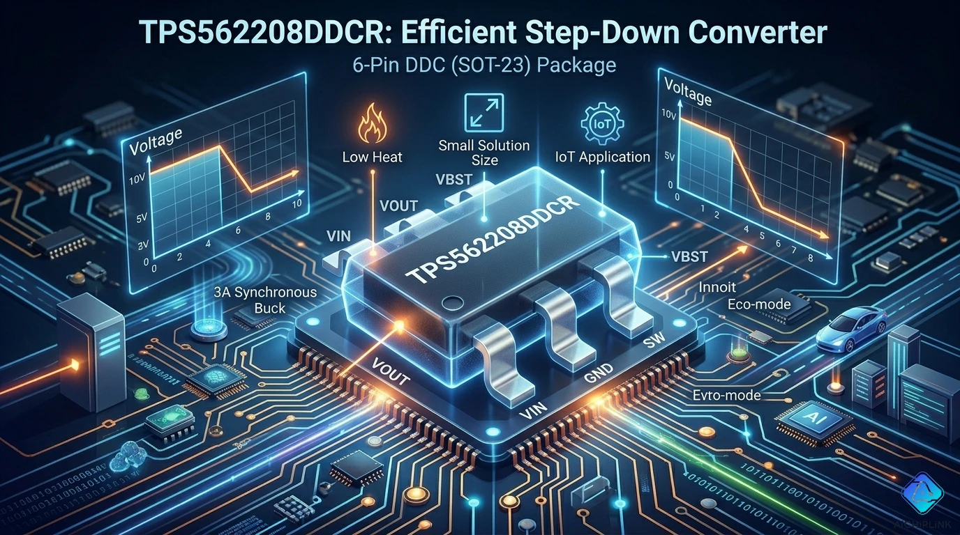
Pin assignments — SOT-23-6 (DDC package):
| Pin | Name | Function |
|---|---|---|
| 1 | VFB | Feedback voltage input — connect resistor divider center tap here |
| 2 | EN | Enable — logic high enables output; pull to VIN via 100 kΩ for always-on |
| 3 | GND | Ground |
| 4 | SW | Switch node — connect inductor here; high di/dt node, keep trace short |
| 5 | VIN | Supply input (4.5V to 17V) |
| 6 | VBST | Bootstrap — connect 0.1 µF ceramic from VBST to SW (mandatory) |
2.0 Three Questions Before You Specify This Part
Question 1: What is your load current profile — heavy load most of the time, or light load most of the time?
TPS562208 uses FCCM. When output current falls below the level where inductor current would naturally reach zero, the low-side FET continues conducting — pulling inductor current negative and recirculating energy. Switching frequency stays roughly constant at ~580 kHz regardless of load. This means:
At heavy load (above roughly 300–500 mA): TPS562208 and TPS562201 behave essentially identically — both are in continuous conduction mode.
At light load (below ~100 mA): TPS562208 stays in CCM, dissipating switching losses even for a tiny load. TPS562201 enters Eco-mode, the low-side FET turns off when inductor current reaches zero, pulses are skipped, and switching losses drop substantially.
If your application spends significant time below 200 mA — a battery device, a sleep-mode MCU supply, a standby rail — TPS562201 will extend battery life noticeably. If the load is consistently above 500 mA, both converters behave the same and the FCCM/Eco distinction is irrelevant.
Question 2: Do you have EMI or radiated emissions constraints at specific frequencies?
FCCM (TPS562208) produces a quasi-fixed 580 kHz fundamental plus harmonics at 1.16 MHz, 1.74 MHz, and so on. The energy is concentrated at predictable, discrete frequencies — easier to filter with a targeted LC input filter, but the peaks are higher.
Eco-mode (TPS562201) at light load spreads switching energy across a wider spectrum as the effective pulse rate varies. Peak amplitude is lower but spectral content is less predictable.
If a 580 kHz harmonic lands in a sensitive reception band of an adjacent RF circuit, or if your product must pass radiated emissions testing with a strict limit at that frequency, evaluate TPS562201. If the fixed-frequency spectrum is acceptable or easier to filter in your design, TPS562208 is fine.
Question 3: Is your output supply rail noise-sensitive at low frequencies?
FCCM: output ripple is regular and predictable at all loads — constant frequency, varying amplitude. No sub-audio-frequency ripple.
Eco-mode: at light load, the effective switching rate decreases as pulses skip. This can introduce ripple at frequencies potentially in the audible range for very light loads. For precision ADC reference rails, PLL supply rails, or audio circuits powered from the converter output, FCCM (TPS562208) is the correct choice regardless of efficiency considerations.
Summary table:
| Load profile | EMI concern at 580 kHz | Output noise sensitivity | Choose |
|---|---|---|---|
| Mostly > 300 mA | None | Low | Either (TPS562208 or TPS562201) |
| Mostly < 200 mA | None | Low | TPS562201 (better efficiency) |
| Any | Yes — 580 kHz problematic | Low | TPS562201 |
| Any | No | High (ADC ref, audio, PLL) | TPS562208 (predictable ripple) |
| Any | No | Low | TPS562208 (simpler EMI filtering) |
3.0 Decision Matrix: TPS562208 vs TPS562201 vs Newer TI Alternatives
| Parameter | TPS562208 (FCCM) | TPS562201 (Eco-mode) | TPS562247 (newer) |
|---|---|---|---|
| Max output current | 2A | 2A | 2A |
| Input voltage | 4.5–17V | 4.5–17V | 4.2–17V |
| Output voltage | 0.768V–7V | 0.768V–7V | 0.76V–7V |
| Package | SOT-23-6 (DDC) | SOT-23-6 (DDC) | SOT-563 (smaller) |
| Light-load mode | FCCM | Eco-mode (pulse skip) | FCCM |
| Switching frequency | ~580 kHz | Variable at light load | ~1.2 MHz |
| External compensation | Not required | Not required | Not required |
| Soft-start | 1 ms internal | 1 ms internal | Internal |
| Power-good pin | Not available | Not available | Not available |
| Price (~1k units) | ~$1.30 | ~$1.30 | ~$1.40 |
| Best for | Predictable EMI, analog rails | Battery, light-load efficiency | Space-constrained new designs |
TI's TPS562247 (SOT-563, 1.2 MHz FCCM) offers the same 2A FCCM behavior in a slightly smaller package with higher switching frequency, enabling smaller passive components. For new designs where PCB area is tight, TPS562247 is worth considering. For designs already committed to the 6-pin DDC footprint, TPS562208/TPS562201 are the correct choice.
4.0 Complete Design: Feedback Resistors, Inductor, and Capacitors
Feedback resistor calculation — setting VOUT:
VOUT = 0.768V × (1 + R1/R2)
Where R1 connects VOUT to VFB, and R2 connects VFB to GND. Use 1% tolerance resistors for both. Recommended R2 range: 10 kΩ to 100 kΩ.
| VOUT Target | R2 | Calculated R1 | Nearest 1% E96 | Actual VOUT |
|---|---|---|---|---|
| 1.05V | 10 kΩ | 3.69 kΩ | 3.74 kΩ | 1.055V |
| 1.2V | 10 kΩ | 5.63 kΩ | 5.62 kΩ | 1.199V |
| 1.8V | 10 kΩ | 13.45 kΩ | 13.3 kΩ | 1.790V |
| 3.3V | 10 kΩ | 32.97 kΩ | 33.2 kΩ | 3.318V |
| 5.0V | 10 kΩ | 55.21 kΩ | 54.9 kΩ | 4.992V |
Inductor selection:
Target 20–40% peak-to-peak ripple current relative to maximum output current. For VOUT = 3.3V, VIN = 12V, IOUT = 2A, f_SW = 580 kHz, targeting ΔIL = 0.6A (30%):
L = VOUT × (VIN − VOUT) / (VIN × f_SW × ΔIL) = 3.3 × 8.7 / (12 × 580,000 × 0.6) = 6.87 µH
Use nearest standard value: 6.8 µH or 10 µH. For lower output voltages (1.05V from 5V), the on-time is longer and frequency lower — a smaller inductor (2.2–3.3 µH) is appropriate.
Inductor requirements: saturation current ≥ IOUT + ΔIL/2 (minimum 2.3A, use 3A-rated for margin); DCR ≤ 50 mΩ; shielded construction preferred to minimize radiated EMI from the switch node.
Output capacitor selection:
D-CAP2 is optimized for low-ESR ceramic (X5R/X7R) or polymer (POSCAP, SP-CAP) capacitors. Standard aluminum electrolytic capacitors are not suitable — see Mistake 1 below. TI recommends 20–68 µF total output capacitance.
For a 3.3V/2A design: two 22 µF X5R 0805 ceramics in parallel (total 44 µF, ESR ≈ 1 mΩ combined) gives approximately 3.5 mV peak-to-peak output ripple.
Input capacitor: ≥ 10 µF X5R/X7R ceramic at VIN pin, voltage-rated ≥ VIN_max with 25% margin. Add optional 0.1 µF for high-frequency bypass. For a 12V input design, use 16V or 25V rated capacitors (avoid Y5V/Z5U dielectrics — they lose capacitance under DC bias).
Bootstrap capacitor (mandatory): 0.1 µF X5R/X7R ceramic between VBST (pin 6) and SW (pin 4), placed within 1 mm of both pins. Without it, the high-side FET will not switch.
5.0 ⚠️ Four Field-Killing Mistakes With This Part
Mistake 1: Using electrolytic capacitors on the output
D-CAP2 control is stable with ceramic and low-ESR polymer capacitors. It is not designed for standard aluminum electrolytic capacitors. Engineers who substitute a 100 µF electrolytic "for more capacitance" find the converter oscillates or produces excessive output ripple. The D-CAP2 loop uses an internal ripple injection circuit calibrated for near-zero-ESR outputs; a real high-ESR electrolytic interacts with this in an uncontrolled manner. Use ceramic (X5R or X7R) or POSCAP/SP-CAP polymer types exclusively.
Mistake 2: Leaving the EN pin floating
If EN is left floating, the device behavior is indeterminate — it may start, may not, may oscillate. For an always-on design, connect EN to VIN through a 100 kΩ pull-up resistor. The resistor allows future enable control if needed and limits any transient EN pin current. Do not connect EN directly to VIN without a resistor.
Mistake 3: Running the VFB sense trace near the SW node
The VFB pin is a high-impedance node measuring a small voltage (0.768V). A PCB trace from the feedback resistor divider to VFB that runs alongside or near the SW node picks up high-frequency switching transients, injecting noise directly into the feedback loop. Route the VFB trace on the opposite side of the PCB from the SW node and inductor, or at a minimum, route it orthogonally and with as much separation as the layout allows. Place R1 and R2 physically close to the VFB pin.
Mistake 4: Choosing TPS562208 for battery-powered designs and then wondering why standby current is high
In a design where the load drops to 10–50 mA during sleep, FCCM keeps the converter switching at ~580 kHz continuously, maintaining non-trivial switching losses. The efficiency at 10 mA load in FCCM mode can be below 50%, versus 80–90% for an Eco-mode part at the same light load. For any design with significant sleep or standby operating time, the efficiency difference between TPS562208 and TPS562201 below 200 mA load is the dominant factor in battery life — not the heavy-load efficiency.
6.0 Pre-Tape-Out Checklist
- VOUT feedback resistors calculated: 1% tolerance, R2 in range 10–100 kΩ
- Correct part chosen: TPS562208 (FCCM) or TPS562201 (Eco-mode) per Sections 2 and 3
- Bootstrap capacitor: 0.1 µF X5R/X7R placed within 1 mm of VBST and SW pins
- Input capacitor: ≥ 10 µF ceramic, rated ≥ VIN_max × 1.25, X5R or X7R dielectric
- Output capacitor: ceramic or polymer only, 20–68 µF total, ESR < 10 mΩ, voltage rated ≥ VOUT × 1.5
- Inductor: Isat ≥ 2.3A, DCR ≤ 50 mΩ, value per switching frequency and ripple calculation
- EN pin connected — not floating; pulled to VIN via 100 kΩ if always-on
- SW node trace: short, wide, direct from pin 4 to inductor — not shared with any signal trace
- VFB trace routed away from SW node; sensing at output capacitor positive terminal
- Ground star: input cap GND, output cap GND, device GND (pin 3) joined at one low-impedance point
- Thermal check: P_diss = (VIN − VOUT)/VIN × VIN × IOUT × (1 − η); Tj = TA + P × θJA; confirm ≤ 125°C (θJA ≈ 230°C/W for DDC package in still air)
7.0 Real Questions from Circuit Designers
Q: My TPS562208 output is oscillating at about 50 kHz with 100 mV peak-to-peak. Input is 12V, output is 5V at 500 mA. What is wrong?
A: The most likely cause is an incompatible output capacitor. Verify you are using ceramic or low-ESR polymer — aluminum electrolytics cause exactly this oscillation with D-CAP2. Also verify total output capacitance is in the 20–68 µF range; too little or too much capacitance can each cause loop issues. Second possibility: the VFB trace is picking up switching noise from the SW node, injecting spurious feedback. Third: confirm the 0.1 µF bootstrap capacitor is correctly placed between VBST and SW — a missing or misplaced bootstrap cap causes erratic high-side switching that can manifest as low-frequency ripple.
Q: Can I use TPS562208DDCR to generate 3.3V from a 3.7V LiPo battery?
A: The minimum input voltage for TPS562208 is 4.5V. A fully charged LiPo is 4.2V — already below the 4.5V minimum. At nominal (3.7V) and discharged (3.0V), operation is further outside spec. TPS562208 is not suitable for direct LiPo input. For single-cell LiPo to 3.3V, use a true LDO if current is modest (e.g., AP2112K, MCP1700), or a buck converter with a lower minimum input such as TI's TPS63020 (down to 1.8V input) or TPS62840 (down to 1.8V, 200 mA).
Q: DDCR is backordered. Can I use DDCT as a direct replacement?
A: Yes, without any design changes. DDCR and DDCT are the same silicon die in the same package (SOT-23-6 DDC), with the only difference being reel count — 3,000 per reel for DDCR versus 250 per reel for DDCT. Electrical performance, pinout, and all specifications are identical. DDCT may also be available as cut tape in small quantities from distributors. Substitute freely.
8.0 Quick Reference Card
Part Number Decoded:
| Field | Characters | Meaning |
|---|---|---|
| Family | TPS5622 | TI D-CAP2 2A SOT-23 buck |
| Mode | 08 | FCCM (no pulse skip) |
| Package | DDC | SOT-23-6 Thin, 1.6×2.9 mm |
| Packaging | R | Tape-and-Reel, 3,000/reel |
Key Specifications:
| Parameter | Value |
|---|---|
| VIN range | 4.5V to 17V |
| VOUT range | 0.768V to 7V (adjustable) |
| IOUT max | 2A |
| VFB reference | 0.768V |
| f_SW (FCCM) | ~580 kHz |
| High-side RDS(on) | 140 mΩ |
| Low-side RDS(on) | 84 mΩ |
| Soft-start | 1 ms (internal) |
| Temp range (Tj) | −40°C to +125°C |
VOUT Formula: VOUT = 0.768 × (1 + R1/R2) — use 1% resistors
The one decision that matters most:
TPS562208 (08 = FCCM): fixed 580 kHz, predictable EMI, stable output at all loads → use for noise-sensitive rails and heavy-load applications
TPS562201 (01 = Eco-mode): pulse-skip at light load, lower light-load dissipation → use for battery-powered designs and light-load efficiency priority
For sourcing Texas Instruments TPS562208DDCR with verified authenticity and competitive pricing, visit aichiplink.com.

Written by Jack Elliott from AIChipLink.
AIChipLink, one of the fastest-growing global independent electronic components distributors in the world, offers millions of products from thousands of manufacturers, and many of our in-stock parts is available to ship same day.
We mainly source and distribute integrated circuit (IC) products of brands such as Broadcom, Microchip, Texas Instruments, Infineon, NXP, Analog Devices, Qualcomm, Intel, etc., which are widely used in communication & network, telecom, industrial control, new energy and automotive electronics.
Empowered by AI, Linked to the Future. Get started on AIChipLink and submit your RFQ online today!
Frequently Asked Questions
What applications is TPS562208DDCR best suited for?
TPS562208DDCR from Texas Instruments is a 2A synchronous buck converter ideal for industrial systems, networking equipment, and analog/RF power rails where stable switching frequency and predictable noise performance are critical, especially under medium-to-high load conditions.
How do I choose between TPS562208 and TPS562201?
The key difference is operating mode: TPS562208 uses FCCM (fixed frequency, stable ripple), while TPS562201 uses Eco-mode (better efficiency at light load). Choose TPS562201 for battery-powered or low-load applications, and TPS562208 for noise-sensitive or consistently higher-load designs.
How is the output voltage set?
The output voltage is configured using a resistor divider with the formula: VOUT = 0.768 × (1 + R1/R2). By selecting appropriate resistor values, you can easily set common voltages like 1.2V, 3.3V, or 5V.
What are the most common design mistakes?
Typical issues include using high-ESR electrolytic capacitors, leaving the EN pin floating, routing the feedback trace near the SW node, and using FCCM in light-load battery designs—these can lead to instability, noise, or poor efficiency.
Can TPS562208DDCR be used with a Li-ion battery?
No. The device requires a minimum input of 4.5V, while a typical Lithium-ion battery operates between 3.0V and 4.2V, which is below the required range. A low-input buck or buck-boost converter should be used instead.


