The premise in the title deserves some interrogation before you read any further. CMOS, BSI CMOS, and Stacked CMOS are not three competing options sitting on a shelf waiting for you to pick the winner. They are three generations of the same core technology, each solving a specific limitation of the one before it. Asking which is "best" is like asking whether a screwdriver is better than the same screwdriver with a ratchet mechanism and a magnetic bit holder. Technically yes — but only when the problem you are solving requires what the additions provide.
Here is the real picture: traditional front-side illuminated (FSI) CMOS sensors do exactly what they were designed to do, efficiently and cheaply, and remain the right choice for applications where pixel size is large and light is plentiful. BSI CMOS resolved the fill factor problem that plagued FSI sensors as pixels shrank past a certain size threshold, and it now dominates smartphones and compact cameras almost entirely. Stacked CMOS then separated the problem of light capture from the problem of data processing — and in doing so unlocked capabilities (960 fps video, global shutter at full resolution, on-sensor AI inference) that had nothing to do with image quality and everything to do with readout speed.
Understanding which sensor to use — or which sensor is inside a device you are evaluating — requires understanding what each architecture actually solves, and what it trades off to get there.
1.0 Traditional CMOS (FSI): The Architecture Everything Else Evolved From
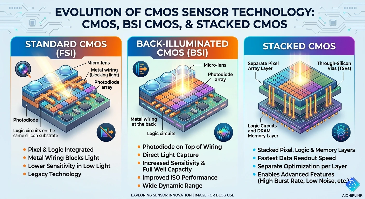
A traditional CMOS image sensor — technically called a front-side illuminated (FSI) sensor — works by directing light through the front face of the silicon wafer, where it passes a series of metal wiring layers and transistors before reaching the photodiode that actually converts light into an electrical charge.
Each pixel in an FSI CMOS sensor contains several sub-components stacked from top to bottom: a microlens to focus incoming light, a color filter (red, green, or blue in a Bayer pattern), the metal interconnect wiring and read-out transistors, and at the bottom, the photodiode itself.
The fundamental limitation of this architecture is the fill factor — the ratio of light-sensitive area (the photodiode) to total pixel area. The metal wiring and transistors occupy space at the top of each pixel, directly in the light path. For large pixels (above roughly 3–4 micrometers), microlenses can compensate by bending incoming light toward the photodiode and achieving acceptable fill factors of 60–70%. For small pixels below about 2 micrometers — the size now common in smartphone cameras — the wiring layers block a proportionally larger fraction of incoming light, and no amount of microlens optimization fully compensates.
Where FSI CMOS is still the right choice: Industrial machine vision cameras, scientific imaging systems, astronomy detectors, and medium-to-large format digital cameras where pixel pitch is 5 micrometers or larger. At those pixel sizes, FSI provides perfectly adequate light collection, and the simpler (and therefore cheaper) manufacturing process is a genuine advantage. FSI sensors above roughly 2 megapixels tend to give way to BSI in modern designs, but below that threshold FSI remains common precisely because it is cost-effective and technically sufficient.
2.0 BSI CMOS: Solving the Fill Factor Problem
Back-side illuminated (BSI) CMOS sensors solve the fill factor problem through a conceptually simple but manufacturing-intensive change: the wafer is flipped during fabrication. After the photodiodes and wiring are built using standard semiconductor processing, the silicon substrate on which they were fabricated is mechanically thinned from the back side until the photodiodes sit near the surface. Light then enters from the back (now the top) of the thinned wafer, reaching the photodiode directly — without passing through any wiring layers at all.
The result is dramatic for small pixels. By removing the wiring obstruction from the light path, BSI sensors can achieve fill factors approaching 100% — meaning nearly the entire pixel area is light-sensitive. The improvement from FSI to BSI is most pronounced for pixels smaller than about 1.4 micrometers, which is why BSI became the standard for smartphone cameras as pixel sizes shrank through the 2010s to hit 1.0 μm, 0.8 μm, and now 0.7 μm in leading flagship sensors.
What BSI actually changes in practice:
- Quantum efficiency (the fraction of incoming photons that become electrons) increases from roughly 60% in FSI to over 90% in BSI for small pixels
- Low-light signal-to-noise ratio improves substantially, typically 1–2 stops in equivalent sensor performance
- Angular light acceptance improves — BSI sensors respond better to light arriving at oblique angles, relaxing lens design constraints for compact modules
- Color fringing at the edges of wide-angle images decreases because off-axis light reaches photodiodes more uniformly
The trade-offs BSI introduces:
- Manufacturing complexity increases significantly: thinning the wafer from the back is a precision process that affects yield
- The thinned silicon behind the photodiode has a surface closer to the active region, which can cause interface traps — electrically active defects that introduce dark current and noise, particularly in dark conditions
- Pixel-to-pixel crosstalk can increase: light entering one pixel can scatter into adjacent pixels through the thin silicon layer, reducing color accuracy and sharpness. Industry solutions include deep trench isolation (DTI) etched between pixels to reduce this effect
Sony was first to introduce a consumer BSI sensor at scale in 2009 with the Exmor R, initially in compact cameras and quickly adopted in the iPhone 4. Over 90% of modern smartphones now use BSI sensors — a market share figure that reflects the technology's decisive advantage for the small pixel sizes required in thin mobile devices.
3.0 Stacked CMOS: Solving the Readout Speed Problem
BSI CMOS solved light collection. Stacked CMOS solves a different problem: the speed at which the captured image data can be read out of the sensor and processed.
In both FSI and BSI sensors, the pixel array and the signal processing circuitry share the same silicon die. This architectural constraint limits the complexity and speed of the on-chip processing — adding more transistors for faster readout means fewer or smaller photodiodes, which harms image quality. The two requirements (more light collection, more processing capability) compete for the same silicon real estate.
Stacked CMOS resolves this by fabricating the pixel layer and the logic/processing layer on separate wafers, then bonding them face-to-face (or in successive layers) using copper-to-copper interconnects at high density. Each layer is then free to be optimized for its specific function without trading off against the other.
Sony commercialized this architecture in 2012 as the Exmor RS. The key capability that stacked CMOS unlocked was not better image quality — early stacked sensors matched but did not exceed BSI sensors in static image quality — but dramatically higher readout speed:
- A conventional BSI sensor reads pixel data row by row, which takes time. During a fast pan or with a fast-moving subject, the bottom of the frame is captured measurably later than the top, producing the characteristic "rolling shutter" skew where vertical lines tilt diagonally
- A stacked sensor with on-chip DRAM buffer can read the entire frame nearly simultaneously (approaching "global shutter" behavior), eliminating most rolling shutter distortion
- The added DRAM layer also acts as an ultra-fast buffer, enabling very high frame rate video (Sony achieves 960 fps at reduced resolution, Canon's EOS R3 captures 30 fps full-resolution with minimal blackout using this architecture)
- The separate logic layer can incorporate on-chip ISP (image signal processor) functions, enabling HDR merging, AI-driven noise reduction, and real-time subject tracking at the sensor level before data leaves the chip
Canon's EOS R3, EOS R5 Mark II, Nikon's Z9 and Z8 (which use a Sony stacked sensor), and Sony's A1 all use stacked BSI CMOS — the combination of BSI light collection efficiency with stacked-architecture readout speed. The Canon EOS R1 and R5 Mark II pair their stacked sensor with a dedicated "DIGIC Accelerator" chip that further boosts the sensor's data processing throughput.
4.0 Head-to-Head Specifications
| Characteristic | FSI CMOS | BSI CMOS | Stacked CMOS |
|---|---|---|---|
| Light path | Through wiring layers | Direct to photodiode | Direct (BSI base) |
| Fill factor | 60–70% (small pixels) | ~90–100% | ~90–100% |
| Quantum efficiency | ~60% (1μm pixel) | ~90% (1μm pixel) | ~90% (same as BSI) |
| Low-light performance | Reference | +1–2 stops vs FSI | Same as BSI |
| Rolling shutter | Significant | Moderate | Greatly reduced |
| Max readout speed | Limited by shared silicon | Moderate | Very high |
| High frame rate video | Limited | Moderate | Exceptional (up to 960fps) |
| On-chip processing | Basic | Moderate | Full ISP, AI, DRAM buffer |
| Pixel crosstalk | Low (thick silicon) | Higher (requires DTI) | Higher (requires DTI) |
| Manufacturing cost | Lowest | Medium | Highest |
| Typical pixel size | ≥ 3μm | 0.7–3μm | 0.7–2μm |
| Typical application | Industrial, large-format | Smartphone, compact | Pro mirrorless, flagship phone |
| Example products | Industrial cameras, astronomy | iPhone 14 camera, Galaxy S23 | Sony A1, Canon EOS R3, iPhone 15 Pro |
5.0 The Real Differences: What Actually Changes Between Generations
FSI → BSI: Everything changed for small pixels, almost nothing changed for large pixels
The benefit of BSI is greatest when pixels are small. A large-pixel sensor (5μm or larger) in a full-frame or medium-format camera already has a high fill factor in FSI configuration, because the wiring layer occupies a small fraction of the large pixel area. The "up to 2× low-light improvement" commonly cited for BSI is measured on small pixels in smartphone sensors. On the large sensors in full-frame cameras, the improvement exists but is more modest — which is why BSI adoption in full-frame interchangeable-lens cameras lagged smartphones by many years. The Sony A7R II (2015) was notable partly because it brought BSI to a large full-frame sensor, where the improvement over the already-capable FSI sensor was measurable but not transformative.
BSI → Stacked: Image quality stayed largely the same; speed changed fundamentally
This is the most important and least-understood distinction. Stacked CMOS sensors in professional mirrorless cameras do not produce significantly better individual still images than equivalent BSI sensors in terms of resolution, dynamic range, or high-ISO noise performance. The sensor stack does not improve any of those parameters. What it does is enable the camera to operate in ways that were impossible before — essentially global shutter performance, blackout-free continuous shooting at 20–30 fps, and 4K/8K video without rolling shutter artifacts at full frame. If you are shooting landscape photography with a tripod and a slow shutter speed, you would be hard-pressed to see a difference between a BSI image and a stacked CMOS image at equivalent resolution and aperture. If you are shooting a falcon diving at 200 mph with an electronic shutter at 20 fps, the difference is everything.
The three-way comparison that is genuinely meaningful:
| Scenario | FSI Verdict | BSI Verdict | Stacked Verdict |
|---|---|---|---|
| 12MP smartphone camera, 0.8μm pixels | ❌ Too noisy | ✅ Ideal | ✅ Ideal + faster video |
| 50MP full-frame mirrorless, 4μm pixels | ✅ Adequate | ✅ Better | ✅ Better + speed |
| 4K/120fps smartphone video | ❌ Rolling shutter | ⚠️ Some rolling shutter | ✅ Minimal rolling shutter |
| Machine vision industrial camera, 3μm | ✅ Good | ✅ Better SNR | ⚠️ Overkill/expensive |
| 32MP 960fps sports camera | ❌ Impossible | ❌ Too slow | ✅ Only viable option |
| Low-cost IoT camera module, 1.3MP | ✅ Cost-effective | ✅ Better | ❌ Unnecessary cost |
6.0 ⚠️ Three Ways Sensor Marketing Misleads Buyers
Pitfall 1: "BSI sensor" in a spec sheet does not tell you the pixel size — which is the only thing that tells you whether BSI actually matters
Marketing materials uniformly tout BSI as an advantage without disclosing whether the pixel size is small enough for BSI to provide meaningful benefit. A 13MP 1/2.3" sensor with 1.1μm pixels genuinely benefits from BSI — the improvement is real and measurable. A 24MP full-frame sensor with 6μm pixels benefits from BSI by a much smaller margin. If you are evaluating a camera based on "BSI sensor" in the spec sheet without checking pixel size, you are using incomplete information. For pixels larger than roughly 3μm on a well-designed sensor, the BSI advantage in light collection is modest. The spec that matters most alongside sensor type is pixel pitch in micrometers or the combination of sensor size and megapixel count.
Pitfall 2: "Stacked CMOS" is treated as synonymous with "better image quality"
It is not. Stacked CMOS is primarily a speed technology. In a controlled static-image comparison (tripod, good light, base ISO), a high-quality BSI sensor and a stacked CMOS sensor of equivalent resolution and pixel size will produce images that are essentially indistinguishable. The stacked sensor wins decisively in burst rate, video rolling shutter, and computational photography throughput — not in the fundamental photographic quality of a single well-exposed frame. Professional photographers who primarily shoot landscapes, portraits, or studio work see modest real-world benefit from paying the price premium that stacked CMOS sensors command. Sports, wildlife, and video professionals see enormous benefit.
Pitfall 3: All three types are "CMOS" — the CMOS label itself is nearly meaningless as a differentiator
BSI is a CMOS sensor. Stacked CMOS is a CMOS sensor. When a camera manufacturer simply says "CMOS sensor" without specifying FSI, BSI, or stacked, they are telling you almost nothing about the sensor's capability. All mainstream digital cameras since roughly 2010 use CMOS sensors. The distinction that matters is which generation of CMOS architecture — and at what pixel size, sensor size, and readout speed. A spec sheet that says "24MP CMOS" could describe anything from a budget webcam to an industrial vision sensor to a smartphone with a 0.7μm pixel BSI chip.
7.0 Decision Guide: Which Architecture for Which Application
When FSI CMOS is the right choice:
- Industrial machine vision cameras where pixel size is ≥ 3μm and light is controlled
- Scientific and astronomical imaging where large pixel area is fundamental to sensitivity
- Low-cost camera modules where pixel count is low (< 2MP) and cost matters more than ultimate performance
- Specialized imaging (X-ray, infrared) where other considerations dominate sensor architecture choice
When BSI CMOS is the right choice:
- Any camera where pixels are smaller than approximately 2μm — this covers essentially all smartphone cameras
- Compact camera modules where physical space prevents larger sensors
- Security and surveillance cameras needing good low-light performance in a small, economical package
- Consumer cameras at all levels where rolling shutter from electronic shutter is acceptable
When Stacked CMOS is the right choice:
- Professional mirrorless cameras targeting sports, wildlife, and action photography requiring 20+ fps burst rates
- Video cameras where rolling shutter in high-resolution 4K/8K recording is unacceptable
- Smartphone flagship cameras where on-sensor AI processing, HDR video, and 4K/120fps or faster video are primary features
- Applications where near-global shutter behavior is needed without the sensitivity penalty of a true global shutter sensor
When NOT to pay the stacked CMOS premium:
- Primary use is landscape, portrait, or studio photography where burst rate and rolling shutter are irrelevant
- Budget or mid-range consumer cameras where the cost of stacked CMOS would be better spent on a larger sensor or better lens
- Industrial applications where BSI provides adequate SNR at lower system cost
8.0 Sourcing Image Sensors: What Engineers and Designers Actually Buy
For product designers and engineers integrating image sensors into cameras, smartphones, automotive systems, or industrial equipment, the primary sensor manufacturers supplying image sensor die or modules are Sony Semiconductor Solutions (Exmor R, Exmor RS), OmniVision Technologies (OV series), Samsung Semiconductor (ISOCELL), and ON Semiconductor (AR series for industrial/automotive).
Sony's Exmor R series covers BSI from smartphone to full-frame. Sony's Exmor RS series covers stacked BSI from smartphone to professional camera. OmniVision's BSI sensors dominate the compact camera module market. Samsung's ISOCELL series is used in Samsung Galaxy devices and sold to other smartphone OEMs. For automotive ADAS, ON Semiconductor's AR0820 and similar sensors provide BSI CMOS with AEC-Q100 qualification.
For verified authentic image sensor components and competitive pricing across Sony, OmniVision, and Samsung ISOCELL product lines, visit aichiplink.com.
9.0 Real Questions About Image Sensor Selection
Q: My smartphone specs say "BSI sensor." Why do photos still look noisy in low light?
A: BSI improves light collection efficiency relative to FSI at the same pixel size, but it cannot overcome physics. If the sensor is very small (1/4" or smaller) with very small pixels (0.7–0.8μm), even a 90% fill factor BSI sensor captures an absolute amount of light that is tiny. Noise in low light is fundamentally a function of photon count — the fewer photons your sensor gathers in the exposure time, the more statistical shot noise dominates the image. BSI helps by ensuring the sensor captures almost all photons that reach it, but it cannot make more photons arrive. The remaining solution is computational photography (multi-frame noise reduction, Night Mode algorithms) which stacked CMOS makes faster and more capable through on-chip processing.
Q: Nikon's Z9 claims "no mechanical shutter needed" because of its stacked sensor. How does that work?
A: Electronic shutters on conventional BSI sensors produce rolling shutter — different rows of the sensor read out at slightly different times, causing distortion of fast-moving subjects. The Z9's stacked sensor reads out the entire 45.7MP frame fast enough (approximately 1/270 second) to reduce rolling shutter distortion to levels below what most photographers can detect in practical shooting. This is not a true global shutter (which would require all pixels to read simultaneously), but it is fast enough to eliminate the practical problem for almost all subject matter, including professional sports photography. Nikon was therefore confident enough to remove the mechanical shutter entirely, simplifying the camera body and eliminating a wear-prone moving part.
Q: Is a "stacked BSI CMOS" sensor the same as a "3D-stacked CMOS" sensor?
A: Yes — these are the same technology described from different marketing angles. "Stacked BSI" emphasizes that the pixel layer uses back-illumination (BSI), while "3D-stacked" emphasizes the vertical multi-layer architecture. All current commercial stacked sensors use BSI as the pixel layer, because the benefits of stacking (faster readout, more on-chip processing) do not reduce the benefit of BSI (better fill factor). They are complementary, which is why the full name of the architecture is often "stacked BSI CMOS" — BSI for light collection, stacked for processing speed.
Q: For a new industrial inspection camera design, should I use FSI, BSI, or stacked CMOS?
A: For most industrial machine vision applications — component inspection, barcode reading, conveyor vision — a BSI sensor with adequate pixel size (1.5–3μm) provides excellent SNR without the cost premium of stacked. FSI is still appropriate if pixels are large (≥ 3μm) and the higher fill factor of BSI is not needed. Stacked CMOS adds significant cost without benefit for most static or slow-moving inspection applications — unless your system requires very high frame rates (≥ 500fps for high-speed production line inspection) or global shutter behavior to freeze very fast motion without mechanical shutter. In that specific case, a stacked CMOS with near-global-shutter performance is worth the premium. For high-speed inspection, Sony's IMX and Pregius S series sensors are well-established industrial options; for standard vision applications, OmniVision and ON Semiconductor offer cost-effective BSI industrial sensors.
10.0 Quick Reference Card
Three Architectures — Three Different Problems Solved:
| Feature | FSI CMOS | BSI CMOS | Stacked CMOS |
|---|---|---|---|
| Problem solved | Cost-effective baseline | Fill factor at small pixels | Readout speed / processing |
| Fill factor | 60–70% (small pixels) | ~90–100% | ~90–100% |
| Low-light advantage | Reference | +1–2 stops | Same as BSI |
| Rolling shutter | High | Moderate | Low |
| Max frame rate | Low | Moderate | Very high |
| On-chip processing | Basic | Moderate | Advanced (ISP, AI, DRAM) |
| Manufacturing cost | Lowest | Medium | Highest |
| Best pixel size | ≥ 3μm | 0.7–3μm | 0.7–2μm |
The Key Insight:
BSI vs FSI = a light collection question (matters most when pixels < 2μm) BSI vs Stacked = a readout speed question (matters most for video, burst, and AI)
When "BSI" on a spec sheet is misleading: If pixel pitch > 3μm, the fill factor advantage of BSI over FSI is modest and the premium may not be justified. Always check pixel size alongside sensor type.
Historical milestones:
- 2007: OmniVision samples first BSI sensor
- 2009: Sony Exmor R — first consumer BSI sensor (iPhone 4 uses OmniVision BSI)
- 2012: Sony Exmor RS — first stacked CMOS sensor
- 2015: Sony A7R II — first BSI full-frame sensor in mirrorless ILC
- 2020: Sony A1 / Canon EOS R3 — stacked BSI in flagship full-frame pro cameras

Written by Jack Elliott from AIChipLink.
AIChipLink, one of the fastest-growing global independent electronic components distributors in the world, offers millions of products from thousands of manufacturers, and many of our in-stock parts is available to ship same day.
We mainly source and distribute integrated circuit (IC) products of brands such as Broadcom, Microchip, Texas Instruments, Infineon, NXP, Analog Devices, Qualcomm, Intel, etc., which are widely used in communication & network, telecom, industrial control, new energy and automotive electronics.
Empowered by AI, Linked to the Future. Get started on AIChipLink.com and submit your RFQ online today!
Frequently Asked Questions
What is the difference between CMOS, BSI CMOS, and stacked CMOS?
FSI CMOS, BSI CMOS, and stacked CMOS are three generations of sensor technology. FSI is cost-effective, BSI improves light capture for small pixels, and stacked CMOS enhances readout speed and processing capability.
Which image sensor is best: CMOS, BSI, or stacked CMOS?
The best sensor depends on the use case. BSI is ideal for smartphones and low-light, while stacked CMOS is best for high-speed photography and advanced video.
Why is BSI CMOS better for low-light photography?
BSI CMOS improves fill factor and light efficiency. By removing wiring obstruction, it captures more light, delivering better performance in small-pixel sensors.
What is the main advantage of stacked CMOS sensors?
Stacked CMOS significantly improves readout speed. It reduces rolling shutter and enables high frame rate video, burst shooting, and on-sensor processing.
When should you choose FSI CMOS instead of BSI or stacked?
FSI CMOS is best for cost-sensitive and large-pixel applications. It is commonly used in industrial, scientific, and low-resolution imaging where high sensitivity is not critical.


.png&w=256&q=75)