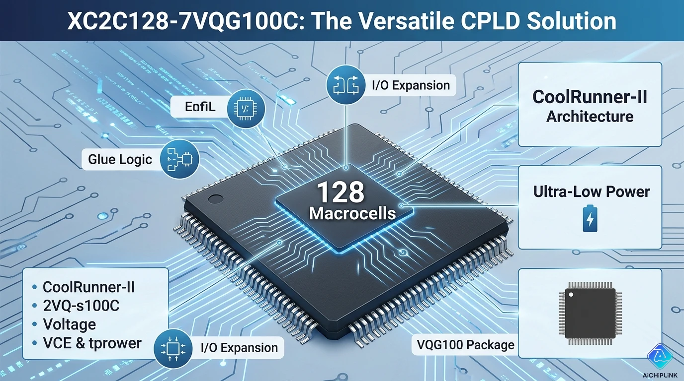
XC2C128-7VQG100C: The "128" Is Macrocells, Not LUTs — and the Difference Determines Everything About This Device
A designer familiar with FPGAs who picks up the XC2C128-7VQG100C datasheet for the first time may go looking for LUT counts, block RAM, and DSP slices. None of those resources exist in this device. The XC2C128 is a CPLD — a Complex Programmable Logic Device — and the 128 in the part number counts macrocells, not look-up tables. The architectural difference between a macrocell and a LUT is not minor: it reflects a fundamentally different logic implementation technology, with different trade-offs in speed, power, configuration behavior, and the types of designs that fit efficiently.
The second thing that surprises engineers encountering CoolRunner-II for the first time: the 100-pin package contains 80 user I/O pins, not 100. The remaining 20 pins are dedicated to power, ground, JTAG programming, and the clock inputs that serve the global clock network. This is not a deficiency — an 80-pin user I/O count in a 14mm × 14mm VTQFP is a very high I/O density — but the discrepancy between package pin count and usable I/O is a specific and common source of confusion during pinout assignment.
The third distinctive characteristic: the XC2C128-7VQG100C stores its configuration in internal non-volatile (Flash-based) memory, powers on at the first clock edge with its logic already active, and draws approximately 100 µW of static power in standby. No external configuration memory. No startup delay. This is what makes CPLDs the right choice for power-on sequencing, glue logic, and boot control — roles where FPGAs with their multi-hundred-millisecond configuration delays and milliwatt-range quiescent power are unsuitable.
1.0 Part Number Decoded: XC2C128-7VQG100C
AMD Xilinx CPLD part numbers follow a structured format encoding the device family, density, speed grade, package, and temperature grade:
XC — Xilinx product prefix (now AMD Xilinx)
2C — CoolRunner-II family identifier. The "2C" distinguishes CoolRunner-II from the original CoolRunner (XC9500 series) and from CoolRunner-XPLA3.
128 — Macrocell count: 128 macrocells — the fundamental measure of logic capacity in a CPLD. The XC2C128 contains 128 macrocells organized into 8 Function Blocks of 16 macrocells each.
-7 — Speed grade: -7 = 7 nanoseconds maximum tPD (propagation delay from input to output through combinatorial logic). CoolRunner-II speed grades available: -4 (fastest), -6, -7, -10 (slowest/lowest power). The -7 grade is the mid-tier: fast enough for most applications without paying for the -4 premium.
V — Package family: V = Very Thin QFP (VTQFP, also called VQFP or VTQFP in Xilinx documentation). Thinner profile than standard QFP.
Q — Package type: Q = Quad Flat Pack (leads on all four sides)
G — RoHS / lead-free indicator: G = lead-free (Pb-free) termination finish. Earlier parts without G suffix used standard SnPb solder.
100 — Pin count: 100 pins total on the package
C — Temperature grade:
- C = Commercial: 0°C to +70°C junction
- I = Industrial: −40°C to +85°C junction (the XC2C128-7VQG100I variant)
Package dimensions (VQG100):
- Body: 14mm × 14mm
- Lead pitch: 0.5mm
- User I/O: 80 pins (of the 100 total pins)
- Package height: Very Thin profile
2.0 Specifications at a Glance
From the Xilinx/AMD XC2C128 CoolRunner-II CPLD datasheet (DS093, v3.2, March 2007):
Logic capacity:
- Macrocells: 128
- Equivalent gates: approximately 3,000 (marketing approximation; gate equivalence for CPLDs is not directly comparable to FPGA LUT-equivalent gates)
- Function Blocks: 8 (each containing 16 macrocells and one 40×56 PLA)
- Product terms per Function Block: 56 (per 16-macrocell block)
Timing (speed grade -7):
- Maximum propagation delay (tPD): 7.0 ns (input to combinatorial output)
- Maximum clock-to-output delay (tCO): 4.5 ns (registered output)
- Maximum system frequency (fSYSTEM): 152 MHz
- Setup time (tSU): 2.5 ns
- Hold time (tH): 0 ns
I/O:
- User I/O (VQG100 package): 80 pins
- Global clock inputs: 4 (dedicated global clock pins — not shared with user I/O in this package)
- I/O voltage standards supported: LVCMOS 3.3V, 2.5V, 1.8V, 1.5V; HSTL Class I; SSTL2 Class I; SSTL3 Class I
- Input tolerance: 5V tolerant on all inputs (can accept 5V logic without damage even with 3.3V VCC)
- Pull-up/pull-down: Configurable per I/O pin
Power:
- VccINT (core supply): 1.8V (1.7V–1.9V)
- VccIO (I/O supply): Per-bank configurable — 1.5V, 1.8V, 2.5V, or 3.3V
- Static (standby) current: approximately 40–100 µA ("Zero Power" standby)
- Dynamic power: Proportional to switching activity and frequency
Configuration:
- Type: Non-volatile internal Flash — configuration persists through power cycles without external memory
- Startup: Instant-on — device is operational at first valid clock edge after power supply reaches VccINT minimum
- In-system programming: IEEE 1532 / JTAG (4-pin: TCK, TMS, TDI, TDO)
Package:
- VTQFP-100 (VQG100), 14mm × 14mm, 0.5mm pitch, Pb-free
3.0 How CoolRunner-II Works: Macrocells, PLA, and the AIM
Why macrocells, not LUTs:
FPGA logic is implemented using lookup tables (LUTs) — small memory arrays that can implement any Boolean function of their inputs by storing the truth table in SRAM. An LUT with 4 inputs can implement any function of 4 variables. LUT-based logic is flexible but volatile (SRAM loses its contents when power is removed) and has relatively high quiescent power.
CPLD logic is implemented using a Programmable Logic Array (PLA) — a two-level AND-OR structure. The PLA takes a set of inputs, generates product terms (ANDs of various input combinations), and then ORs selected product terms to produce output functions. This AND-OR structure maps perfectly to Sum-of-Products (SOP) Boolean expressions, which is the canonical form for combinatorial logic.
The XC2C128 Function Block structure:
Each of the 8 Function Blocks contains:
- A 40×56 PLA: 40 inputs (from the interconnect) × 56 product terms (AND gates). Each of the 56 product terms can be the AND of any subset of the 40 inputs or their complements.
- 16 macrocells: Each macrocell receives selected product terms from the PLA, passes them through an OR gate to produce a sum-of-products output, optionally XORs with another term for inversion, feeds a register (D flip-flop or T flip-flop), and drives an output buffer.
- The 16 macrocells in a Function Block can share the 56 product terms — an output requiring many product terms can "steal" unused product terms from neighboring macrocells within the same Function Block.
The Advanced Interconnect Matrix (AIM):
The 8 Function Blocks are connected by the AIM — a low-power crossbar that routes signals between Function Blocks. The AIM provides each Function Block with access to signals from any other Function Block, enabling designs that span multiple blocks. The AIM is designed for low power (using differential signaling internally) and is the source of CoolRunner-II's "ultra-low dynamic power" characteristic.
Instant-on — the practical impact:
The configuration is stored in on-chip Flash memory. At power-up, there is no configuration loading delay — the device reads its configuration from Flash and is operational within microseconds, before most other devices on the board have completed their power-on sequences. This makes CoolRunner-II the standard choice for:
- Power sequencing: Controlling the order in which supplies ramp on (the CPLD can drive enable pins on LDOs/switching regulators before any other active device is powered)
- System reset management: Generating reset pulses based on power-good signals with guaranteed timing
- Boot arbitration: Deciding which boot source to use before the main processor begins executing
4.0 ⚠️ Four Pitfalls in XC2C128 Designs
Pitfall 1: Exceeding the product term limit for a single output
Each Function Block's 56 product terms are shared among its 16 macrocells. A simple output requiring 2–3 product terms leaves plenty of budget. A complex output requiring 20 product terms consumes 36% of a Function Block's entire product term budget for one output. If multiple complex outputs are assigned to the same Function Block by the place-and-route tool, the product term budget can be exhausted and the tool will either fail to fit the design or insert additional logic levels that increase propagation delay beyond the -7 spec.
The symptom is the Xilinx ISE fitter reporting "resource overflow" or "cannot find a placement that satisfies all constraints" — which can be confusing because the macrocell utilization appears low (say, 60 of 128 macrocells used). The constraint is product terms per Function Block, not macrocell count. Solution: restructure the logic to reduce product terms in complex output equations (use intermediate registers, recode state machines, or use VHDL/Verilog structures that the synthesizer can decompose into fewer product terms).
Pitfall 2: Assuming 5V tolerance means the device operates at 5V logic levels on its I/O
The XC2C128's inputs can withstand 5V voltage levels without damage — but the device core runs at 1.8V and the I/O can only drive outputs at the VCCIO bank voltage (maximum 3.3V). A 5V system can send 5V signals into the XC2C128 inputs (the Schmitt trigger buffers handle this), but the XC2C128 cannot drive 5V logic levels on its output pins. For bidirectional interfaces to 5V devices: the CPLD reads 5V correctly, but the driving voltage is limited to the VCCIO level. For 5V-to-5V bidirectional communication, either accept that the CPLD's output drive at 3.3V will be read as logic high by 5V TTL inputs (3.3V > VIH for 5V TTL = 2.0V) — which often works — or add external level-shifting if the 5V CMOS VIH threshold is a concern.
Pitfall 3: Incorrect JTAG chain configuration blocking in-system programming
The XC2C128's JTAG interface (IEEE 1149.1) serves double duty: boundary scan testing and in-system programming (via IEEE 1532). If other JTAG-capable devices are in the JTAG chain (a processor, an FPGA, another CPLD), the XC2C128 must be correctly positioned in the chain with its IDCODE recognized by the programming software. A common mistake is connecting the XC2C128's TDO to the next device's TDI without verifying that the Xilinx iMPACT (or ISE) tool recognizes the complete chain and can target the correct device. Programming will fail silently if the tool cannot locate the XC2C128 in the chain. Verify the JTAG chain with a boundary scan tool that enumerates all devices before attempting in-circuit programming.
Pitfall 4: Using ISE WebPACK 14.7 on modern OSes without verifying compatibility
The XC2C128-7VQG100C is supported by Xilinx ISE Design Suite (WebPACK Edition, free), with ISE 14.7 being the final version (released 2013). ISE 14.7 was designed for Windows XP/7 and Linux with specific library versions. On modern Linux distributions (Ubuntu 22.04+, Fedora 38+) and Windows 10/11, ISE 14.7 installation and operation requires workarounds — specific library patches, compatibility layers, or running in a virtual machine or container. AMD Xilinx does not officially support ISE on these newer OS versions. If using ISE for CoolRunner-II development on a modern workstation, plan for the compatibility workaround effort: the most reliable approach is Ubuntu 18.04 LTS in a VM, or the community-maintained ISE installation scripts for modern Ubuntu.
5.0 Application Design Notes: Power, I/O, and Tool Setup
Power supply:
The XC2C128 requires two supply voltages:
- VccINT = 1.8V (±0.1V): Core logic supply. Current is small (< 10 mA for most designs at low frequency); use any 1.8V LDO or switching regulator. Decouple with 100 nF X5R/X7R ceramic at the VccINT pins.
- VccIO = 1.5V, 1.8V, 2.5V, or 3.3V: I/O supply, set per-bank based on the interface standard needed. The VQG100 package has one I/O bank — one VccIO voltage for all 80 user I/O pins. If mixed voltage I/O is needed (some pins at 3.3V, others at 1.8V), select a different Xilinx device with multiple I/O banks, or use external level shifters.
I/O bank planning:
The VQG100 package has a single VccIO domain. All 80 user I/O pins share the same output voltage. If the design connects to both 3.3V logic (e.g., a microcontroller) and 1.8V logic (e.g., an SDRAM control interface), a single VccIO cannot serve both at optimal drive levels. For mixed-voltage designs, the XC2C128 in the CPG132 (chip scale BGA) or TQG144 package may offer more I/O bank flexibility — check the datasheet for package-specific bank assignments.
Global clock distribution:
The VQG100 package has 4 dedicated global clock input pins. These feed low-skew clock distribution networks to all macrocell registers across all 8 Function Blocks. For any registered design, always route the primary clock to a global clock pin. Routing a clock through a general I/O pin and the AIM routing fabric adds clock uncertainty that violates setup/hold timing at speed. Use the VERILOG /* synthesis pin_type=CLK */ attribute or VHDL equivalent to direct the synthesizer to use a global clock input.
Tool setup:
Xilinx ISE Design Suite 14.7 WebPACK (free download from AMD's legacy software page) supports CoolRunner-II. It includes XST synthesis, the CPLD fitter, iSim simulation, and iMPACT programming software. VHDL and Verilog are both supported. For new projects:
- Create a new project targeting XC2C128, package VQG100, speed grade -7, commercial temperature
- Add HDL source files or use the schematic editor
- Run synthesis (XST) → verify product term usage in synthesis report
- Run Implementation (Fit) → verify all macrocells fit with timing closure
- Program via iMPACT with a Xilinx Platform Cable USB or compatible JTAG adapter
AMD Xilinx's Vivado design tool does not support CoolRunner-II (Vivado targets 7-series and newer FPGAs/MPSoCs only). ISE 14.7 is the correct and only AMD-supported tool for XC2C128.
6.0 Comparison: XC2C128 Within CoolRunner-II and vs FPGA/LCMXO2
CoolRunner-II density options:
| Device | Macrocells | Max I/O | Speed grades | Notes |
|---|---|---|---|---|
| XC2C32 | 32 | 33 | -4, -6, -7, -10 | Smallest |
| XC2C64 | 64 | 64 | -4, -6, -7, -10 | |
| XC2C128 | 128 | 100 | -4, -6, -7, -10 | This device |
| XC2C256 | 256 | 184 | -4, -6, -7, -10 | |
| XC2C384 | 384 | 240 | -4, -6, -7 | |
| XC2C512 | 512 | 270 | -4, -6, -7 | Largest |
XC2C128-7VQG100C vs XC2C128-7VQG100I:
The only difference is temperature grade: C = 0°C to +70°C junction; I = −40°C to +85°C. Same die, same functional specifications, same package. For industrial or automotive-adjacent applications, specify the I-grade.
CPLD vs FPGA vs LCMXO2 — choosing the right device type:
| Characteristic | XC2C128 (CPLD) | Xilinx Artix-7 (FPGA) | LCMXO2-7000HC (FPGA/PLD) |
|---|---|---|---|
| Logic structure | PLA + macrocells | SRAM LUTs | SRAM LUTs (NV config) |
| Configuration storage | On-chip Flash (NV) | External SPI Flash required | On-chip Flash (NV) |
| Startup time | < 1 ms (instant-on) | 30–500 ms | < 1 ms (instant-on) |
| Static power | ~100 µW | ~50–100 mW | ~10–50 mW |
| Logic capacity | 128 macrocells | 20K–2M+ LUTs | 6,864 LUTs |
| Block RAM | None | Yes | Yes (468 Kb) |
| DSP blocks | None | Yes | Yes |
| Cost | Low (~$5–12) | Higher ($10–100+) | Medium ($10–25) |
| Best for | Glue logic, sequencing, I/O | Complex algorithms | Mid-complexity, instant-on |
For pure glue logic, power sequencing, and interface bridging where design complexity is modest (< 100 product terms of logic), CoolRunner-II remains the most cost- and power-efficient solution. When the design grows to require block RAM, DSP multipliers, or hundreds of LUT-equivalents of state machine logic, migration to FPGA or LCMXO2 is the appropriate path.
7.0 Sourcing XC2C128-7VQG100C
The XC2C128-7VQG100C is an active AMD Xilinx production part, available from authorized distributors (Mouser, DigiKey, Arrow, Avnet). Pricing at standard distribution: approximately $8–15 per unit at 1–100 piece quantities; lower at volume.
Commercial vs Industrial availability: The -7VQG100C (commercial) is more widely stocked than the -7VQG100I (industrial). For designs requiring industrial temperature, verify availability before design commitment; lead times for I-grade can be longer than C-grade from standard distributor stock.
Counterfeit awareness: CoolRunner-II devices appear in the secondary market with falsified speed grade markings (slower -10 devices marked as -7). Verification: program the device with a design that has been timing-analyzed for -7 grade and run at the edge of the speed specification. If the device fails at speeds that a genuine -7 should handle, it is likely a slower grade. The JTAG IDCODE does not encode the speed grade — only the device family and macrocell count — so IDCODE verification alone does not detect speed grade remarking.
For verified authentic AMD Xilinx XC2C128-7VQG100C with competitive pricing, visit aichiplink.com.
8.0 Real Questions from CPLD Designers
Q: My XC2C128 design has 70 macrocells used (55% utilization) but the ISE fitter fails with "cannot fit." How can it fail with only 55% utilization?
A: Macrocell utilization percentage does not tell the whole story for CPLD fitting. The fitter fails when product term resources are exhausted within one or more Function Blocks, even if macrocells are available. A complex output equation that requires many product terms can overflow a single Function Block's product term budget (56 terms across 16 macrocells). The fitter report's "Product Term" section shows the actual product term utilization per Function Block — look for any Function Block near or at 100% product term usage. Solutions: (1) restructure the logic driving the complex output to use fewer product terms (register intermediate results, use XOR decomposition where appropriate); (2) add user location constraints to spread logic across Function Blocks manually; (3) move to a higher-density device (XC2C256) if the design is legitimately complex.
Q: Can I use Vivado or Quartus Prime to develop for XC2C128-7VQG100C?
A: No. AMD Xilinx's Vivado does not support CoolRunner-II or any XC2Cxxx device — it targets 7-series FPGAs and newer only. Intel Quartus Prime supports Intel/Altera devices only. The correct and only AMD-supported development environment for XC2C128 is Xilinx ISE Design Suite 14.7 WebPACK (free). For programming, iMPACT (included in ISE) programs via JTAG. On modern operating systems (Windows 10/11, Ubuntu 20.04+), ISE 14.7 requires specific compatibility steps: on Ubuntu, use the community-maintained ise_14.7_install.sh script; on Windows 10/11, run ISE inside Windows 7 compatibility mode or in a virtual machine.
Q: I want to interface XC2C128-7VQG100C to a 5V AVR microcontroller (ATmega328) and a 3.3V ARM Cortex-M4. Is this possible with a single XC2C128?
A: Yes, with one important caveat. The XC2C128's inputs are 5V tolerant — it can receive 5V signals from the ATmega without any level shifting. The XC2C128's outputs are limited to the VccIO voltage. With VccIO = 3.3V, the outputs drive at 3.3V, which is readable by 5V TTL/LSTTL (VIH = 2.0V; 3.3V > 2.0V, so it registers as logic high). However, some 5V CMOS inputs require VIH ≥ 0.7 × VCC = 3.5V for a 5V supply, which 3.3V does not satisfy. Verify the ATmega's VIH specification for its specific I/O standard before relying on 3.3V drive to a 5V CMOS input. For the ARM Cortex-M4 side, 3.3V VccIO drives 3.3V logic natively with no issue. The configuration — single VccIO at 3.3V, 5V-tolerant inputs — works for most ATmega interfaces because AVR devices typically use TTL input thresholds.
9.0 Quick Reference Card
Part Number Decode:
| Field | Value | Meaning |
|---|---|---|
| XC2C | XC2C | Xilinx CoolRunner-II CPLD family |
| 128 | 128 | 128 macrocells (8 Function Blocks × 16) |
| -7 | -7 | Speed grade: 7 ns propagation delay |
| VQ | VQ | Very Thin Quad Flat Pack (VTQFP) |
| G | G | Lead-free, RoHS compliant |
| 100 | 100 | 100 total pins (80 user I/O + 20 power/JTAG/clk) |
| C | C | Commercial: 0°C to +70°C junction |
Key Specifications:
| Parameter | Value |
|---|---|
| Macrocells | 128 |
| Function Blocks | 8 (16 macrocells each) |
| Product terms per FB | 56 |
| Max frequency | 152 MHz |
| Propagation delay (tPD) | 7 ns |
| Clock-to-output (tCO) | 4.5 ns |
| User I/O (VQG100) | 80 |
| VccINT | 1.8V |
| VccIO | 1.5V–3.3V (configurable) |
| Input tolerance | 5V |
| Static power | ~100 µW |
| Config memory | On-chip Flash (non-volatile) |
| Startup | Instant-on |
| Programming | JTAG (IEEE 1149.1/1532) |
| Design tool | ISE 14.7 WebPACK (free) |
| Temperature | 0°C to +70°C Tj |
Why 80 I/O from 100 pins: 100 pins total − 4 global clocks − ~8 VccINT/GND − ~8 VccIO/GND = 80 user I/O
The Two Critical Resource Limits:
- Macrocells: 128 total → controls output count
- Product terms per Function Block: 56 → controls logic complexity per output group → the real fitting constraint
Commercial vs Industrial:
- VQG100C: 0°C to +70°C → indoor/controlled environments
- VQG100I: −40°C to +85°C → industrial/outdoor; same die
For sourcing AMD Xilinx XC2C128-7VQG100C with verified authenticity and competitive pricing, visit aichiplink.com.

Written by Jack Elliott from AIChipLink.
AIChipLink, one of the fastest-growing global independent electronic components distributors in the world, offers millions of products from thousands of manufacturers, and many of our in-stock parts is available to ship same day.
We mainly source and distribute integrated circuit (IC) products of brands such as Broadcom, Microchip, Texas Instruments, Infineon, NXP, Analog Devices, Qualcomm, Intel, etc., which are widely used in communication & network, telecom, industrial control, new energy and automotive electronics.
Empowered by AI, Linked to the Future. Get started on AIChipLink and submit your RFQ online today!
Frequently Asked Questions
What is XC2C128-7VQG100C used for?
XC2C128-7VQG100C is a 128-macrocell AMD Xilinx CoolRunner-II CPLD designed for instant-on glue logic, power sequencing, reset control, protocol bridging, and system boot management. Unlike SRAM-based FPGAs, it stores configuration in internal non-volatile Flash memory, allowing logic to become active immediately at power-up with ultra-low standby power consumption, making it ideal for embedded control tasks where fast startup and reliability are critical.
What does “128” mean in XC2C128-7VQG100C?
The “128” in XC2C128-7VQG100C refers to 128 macrocells, not LUTs as found in FPGA devices. These macrocells are organized into 8 function blocks of 16 macrocells each and implement logic using programmable sum-of-products architecture. This structure makes the device highly efficient for deterministic control logic and state machines but less suitable for large memory-intensive or DSP-heavy applications.
Why does the 100-pin XC2C128 package provide only 80 user I/O pins?
Although the VQG100 package contains 100 physical pins, only 80 are available as user I/O because the remaining pins are reserved for power rails, grounds, JTAG programming interface signals, and dedicated global clock inputs. This allocation ensures stable operation, low-noise clock distribution, and reliable in-system programming while still delivering high I/O density in a compact 14mm × 14mm VTQFP package.
Can XC2C128-7VQG100C interface with 5V logic devices?
Yes, XC2C128-7VQG100C supports 5V-tolerant inputs, allowing it to safely receive signals from 5V logic systems even when powered at lower voltages such as 3.3V. However, its outputs are limited by the selected VCCIO bank voltage, meaning it cannot actively drive true 5V output levels. In most TTL-compatible systems this is sufficient, but strict 5V CMOS interfaces may require external level shifting.
Which software supports XC2C128-7VQG100C development?
XC2C128-7VQG100C is supported exclusively by AMD Xilinx ISE Design Suite 14.7 WebPACK, which includes synthesis, fitting, simulation, and JTAG programming tools for CoolRunner-II devices. Vivado does not support this CPLD family. Engineers using modern Windows or Linux systems often run ISE 14.7 inside a virtual machine or apply compatibility patches to maintain reliable development workflows.