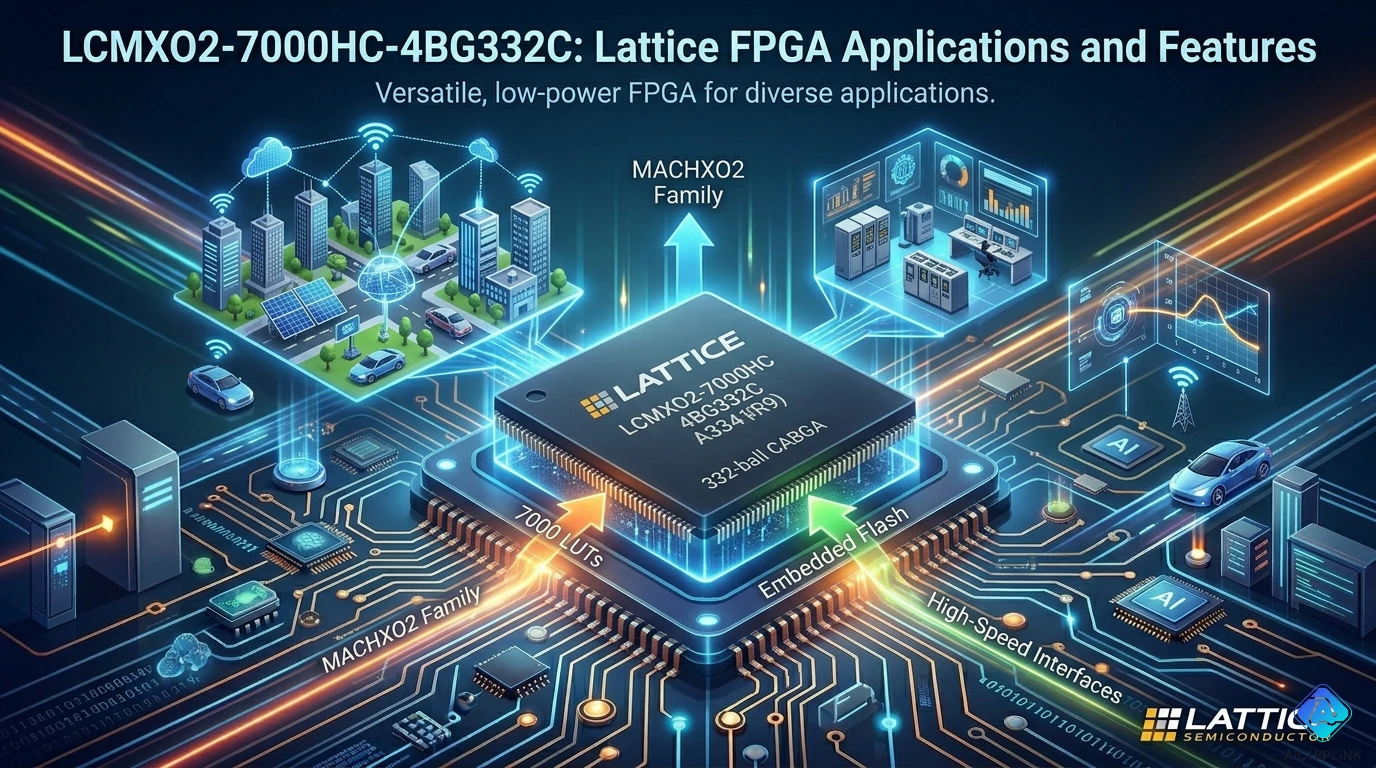
LCMXO2-7000HC-4BG332C: The "7000" Contains 6,864 LUTs — and That Difference Matters More Than You Think
The part number says 7000. The Lattice datasheet says 6,864 LUTs. This is not an error in either document. Lattice's MachXO2 product naming convention rounds to the nearest marketing tier — the device family is called "7000" but the actual look-up table count in the silicon is 6,864. For an engineer estimating logic utilization against a design that fits in 95% of 7,000 LUTs, that 2% shortfall between the marketing number and the actual resource count can mean the difference between a design that fits and a respin to the next density tier.
This naming discrepancy is the first thing to get right when working with this part. The second is understanding what "HC" means, because it changes the power supply design compared to the HE or ZE variants on an adjacent page of the product selector. HC includes an on-chip linear voltage regulator — the device accepts 2.5V or 3.3V at its VCC pins and internally regulates down to the 1.2V logic core. HE and ZE require 1.2V supplied externally. In a 3.3V system, HC eliminates a dedicated 1.2V rail and its associated inductor, capacitor, and regulator — a real BOM and PCB area saving. In a system that already has 1.2V, the internal LDO adds a small inefficiency. Which variant to choose depends on your power architecture.
These two points — actual LUT count versus marketing name, and HC's internal LDO — are the starting context for correctly specifying LCMXO2-7000HC-4BG332C in any design.
1.0 Part Number Decoded: LCMXO2-7000HC-4BG332C Character by Character
Lattice Semiconductor's MachXO2 ordering part number encodes the device family, density tier, power variant, speed grade, package, and temperature grade in a structured string:
LC — Lattice CPLD/FPGA product prefix
MXO2 — MachXO2 family (Machine XO, second generation). The MachXO2 is Lattice's non-volatile instant-on PLD family, positioned between traditional CPLDs and SRAM FPGAs.
-7000 — Density tier identifier. Maps to 6,864 LUTs in actual silicon — the "7000" is a rounded marketing designation, not the literal resource count. Always use 6,864 when estimating resource utilization.
HC — Power variant and voltage regulator option:
- HC = High-performance with internal Core voltage regulator (LDO). Accepts VCC = 2.5V or 3.3V externally; internal LDO generates the 1.2V core voltage. No external 1.2V supply required.
- HE = High-performance External core supply. Requires 1.2V at VCC externally. Same logic performance as HC.
- ZE = Ultra-Zero-power External supply. Optimized for minimum static power. Requires 1.2V. Same function as HC/HE but lower static current.
-4 — Speed grade within the HC family:
- HC speed grades: -4 (slowest), -5, -6 (fastest)
- A speed grade of -4 has the most conservative (slowest) timing specifications but is the most widely stocked and typically the lowest-cost option
- ZE speed grades use -1/-2/-3 numbering (different range, not comparable to HC -4/-5/-6)
B — Package series: B = caBGA (chip-array Ball Grid Array — fine-pitch BGA with solder balls on a chip-scale substrate)
G332 — Package pin count: 332 solder balls in the caBGA-332 (also described as CABGA-332 in distributor listings)
C — Temperature grade:
- C = Commercial (0°C to +85°C junction temperature)
- I = Industrial (−40°C to +125°C junction temperature). The I-grade variant is LCMXO2-7000HC-4BG332I
2.0 Specifications: What the MachXO2-7000HC Actually Contains
All values from Lattice MachXO2 Family Data Sheet (DS1035 / FPGA-DS-02056), MachXO2-7000 row:
Logic:
- LUTs: 6,864 (4-input lookup tables within PFU — Programmable Functional Units)
- Flip-flops / registers: 6,864 (one per LUT)
- Distributed RAM: Derived from LUT fabric, approximately 27 Kb
- Slice/PFU count: 3,432 PFUs (each PFU contains 2 LUT4s and 2 registers)
Memory:
- sysMEM EBR (Embedded Block RAM): 26 blocks × 18 Kb = 468 Kb total block RAM
- Each EBR configurable as single-port RAM, true dual-port RAM, pseudo dual-port RAM, ROM, or FIFO
- UFM (User Flash Memory): Accessible via JTAG, SPI, I²C, or WISHBONE interface — capacity varies; usable as parameter storage, calibration data, firmware staging
Clocking:
- PLLs: 2× sysCLOCK PLL
- PLL input frequency range: 10 MHz to 400 MHz
- Supports fractional-N frequency synthesis, multiply/divide, phase shifting
I/O (BG332 package):
- User I/O pins: 279
- I/O banks: configurable per-bank VCCIO (supports 1.2V, 1.5V, 1.8V, 2.5V, 3.3V)
- Differential I/O support (LVDS, RSDS, BLVDS, mini-LVDS)
- Source-synchronous I/O support (DDR registers at I/O)
- I/O bank power-down capability (individual bank disable for power saving)
Hardened IP (Embedded Function Block, EFB):
- SPI controller: Master/slave SPI (saves ~200 LUTs vs soft implementation)
- I²C controller: Master/slave I²C (saves ~150 LUTs vs soft implementation)
- 16-bit Timer/Counter: With PWM, input capture, compare units
- All EFB functions accessed via WISHBONE interface from user logic
Configuration:
- Non-volatile configuration flash — on-chip, no external configuration memory required
- Instant-on: Configuration loaded from on-chip flash at power-up, no initialization delay
- Dual-boot: Supports two independent configuration images (primary + golden backup)
- TransFR™: Live, in-system reconfiguration without interrupting device operation
- JTAG programming interface (IEEE 1149.1)
- SPI and I²C slave interfaces for in-system programming
Power (HC variant):
- VCC input: 2.5V or 3.3V (nominal)
- Internal LDO generates 1.2V core voltage
- VCCIO: configurable per bank (1.2V–3.3V, independent of VCC)
- Static current (typical): < 5 mA at 3.3V VCC, no I/O switching
Process and package:
- Process: 65nm non-volatile low power
- Package: caBGA-332, approx. 14mm × 14mm body
- Temperature: 0°C to +85°C junction (C grade)
3.0 How MachXO2 Works: Instant-On, Non-Volatile, and Why It Matters
The MachXO2 architecture is fundamentally different from SRAM-based FPGAs (Xilinx Artix, Intel Cyclone, etc.) in one critical way: the configuration is stored in on-chip non-volatile flash memory, not in external SPI flash, not in DRAM that must be initialized, and not in volatile SRAM cells that lose their contents when power is removed.
What "Instant-On" means in practice:
When VCC reaches its operating range, the MachXO2 begins loading its configuration from the on-chip flash in microseconds — not hundreds of milliseconds. The device is operational before most power management chips have finished their own startup sequences. This matters enormously in applications where the PLD must control power sequencing for other devices on the board. An SRAM FPGA that takes 100–500 ms to configure from an external SPI flash cannot perform early-power-up control functions. A MachXO2 can.
Typical LCMXO2-7000HC configuration time: < 1 ms after VCC reaches nominal. Compare to a Xilinx Artix-7 loading from SPI flash: 30–100 ms typical at fast SPI clock speeds.
The non-volatile advantage:
SRAM FPGAs must re-load their configuration every power cycle from external memory. This means: (1) an external flash chip in the BOM, (2) startup latency while the configuration streams over SPI, (3) configuration security complexity (bitstream encryption with external key storage), and (4) a failure mode where corrupted external flash leaves the FPGA unconfigured. The MachXO2's on-chip flash eliminates all four issues at the cost of slightly lower logic density per silicon area compared to pure SRAM FPGA fabric.
Dual-boot and TransFR:
The on-chip flash supports two independent configuration images. The device normally boots from the primary image. If the primary image is corrupted (by an interrupted in-field update, for example), the device can fall back to the golden (secondary) image — a mechanism that makes field firmware updates substantially safer. TransFR (Transparent Field Reconfiguration) takes this further: new configuration data can be loaded into the non-active flash pages while the device continues running from the active configuration, then switched over with a single command — achieving live reconfiguration without any gap in device operation.
4.0 ⚠️ Four Pitfalls in MachXO2-7000HC Designs
Pitfall 1: Sizing the design to "7000 LUTs" and running out of resources
The marketing name "7000" consistently appears in part numbers, selection tools, and vendor descriptions. The actual LUT count is 6,864. A design synthesis report showing 6,701 LUTs used appears to be at 95.7% utilization relative to 7,000 — but is actually at 97.6% relative to 6,864, leaving only 163 LUTs free. Designs at this level of utilization frequently fail to close timing because the place-and-route tool has insufficient routing slack to optimize critical paths. Always use 6,864 as your resource ceiling, and target 80–85% maximum utilization (approximately 5,490 LUTs) to maintain timing margin and ease incremental design changes.
Pitfall 2: Assuming HC and HE are interchangeable with no BOM changes
HC and HE variants are functionally and pin-compatible, but their power supply requirements differ. HC accepts 2.5V or 3.3V at VCC and internally generates the 1.2V core. HE requires 1.2V directly at VCC. Substituting an HC part for an HE (or vice versa) on an existing PCB will result in either an under-voltage condition (HE at 3.3V VCC → internal core at 3.3V, overvoltage) or an over-voltage condition (HC at 1.2V VCC → LDO input below dropout, device fails to regulate) depending on which swap direction. These two variants require different power supply designs. Verify the variant letter before any substitution.
Pitfall 3: Not accounting for EBR initialization data in UFM capacity
When EBR blocks are initialized to non-zero values (pre-loaded with lookup tables, coefficient arrays, or state machine encodings), this initialization data must be stored somewhere — and by default it is stored in the UFM sector of the on-chip flash. Each kilobit of EBR initialization data consumes UFM capacity. If the UFM is also being used as user-accessible non-volatile storage (parameter storage, calibration data), the total UFM capacity can be exceeded, causing Lattice Diamond to issue a configuration overflow error that is not immediately obvious in its cause. In Diamond's Spreadsheet view, set the CONFIGURATION option to "CFG" (stores EBR init in configuration flash, not UFM) to free the full UFM for user data, or set to "CFG_EBRUFM" to split. Initialize EBRs to all-zero where possible — zero-initialized EBRs consume no UFM.
Pitfall 4: Using the wrong Lattice tool version for the BG332 package
Lattice Diamond design tool support for specific packages and device variants has evolved across major versions. The caBGA-332 (BG332) package for MachXO2-7000 requires Diamond 3.x or later; some early Diamond 2.x releases had incomplete BG332 pin assignment files that caused incorrect constraint generation. If the Diamond software reports unfamiliar I/O placement errors or missing bank assignments for BG332 pins, verify that the installed Diamond version matches Lattice's device support matrix for MachXO2-7000 / BG332. The current Lattice Radiant tool also supports MachXO2 devices and is the recommended tool for new MachXO2 designs starting from Radiant 3.0 onward.
5.0 Application Design Notes: Power, I/O, and Tool Setup
Power supply design for HC variant:
The LCMXO2-7000HC-4BG332C requires:
- VCC: 2.5V or 3.3V (nominal), providing input to the internal LDO
- VCCIO (per bank): Independent supply per I/O bank, selectable from 1.2V to 3.3V based on the interface standards used on that bank
- VCCAUX: Internal auxiliary supply (typically derived from VCC via internal LDO in the HC)
Critical decoupling: Place 100 nF X5R/X7R ceramic bypass capacitors within 2 mm of every VCC ball cluster and every VCCIO ball. Add 1–4.7 µF bulk capacitance per power domain on the PCB near the device. Inadequate decoupling causes glitches during configuration loading and during high-activity switching — both of which can manifest as spurious output toggling or failed timing closure in post-silicon validation.
BG332 footprint and PCB stackup:
The caBGA-332 package uses a fine ball pitch (0.5 mm) with 332 balls arranged in a grid. Routing this package requires at minimum a 4-layer PCB with controlled impedance, and more typically 6 layers to allow signal escape from inner ball rows. Place the device with direct fan-out via escaping from the ball array using 0.2–0.25 mm via drill diameter with 0.4 mm pads. Do not attempt to route BG332 on a 2-layer PCB.
I/O bank assignment and VCCIO planning:
The BG332 package has multiple I/O banks, each with its own VCCIO supply. Before assigning pins in Lattice Diamond (or Radiant), map out which interface standards are needed and group them by required VCCIO:
- 3.3V I/O: TTL, LVCMOS33, SPI at 3.3V
- 2.5V I/O: LVCMOS25, most LVTTL legacy interfaces
- 1.8V I/O: LVCMOS18, many modern CMOS interfaces, DDR at 1.8V
- Differential (LVDS, RSDS): Typically assigned to banks that support differential I/O; VCCIO for differential bank is usually 2.5V or 3.3V
Banks cannot mix VCCIO voltages — all I/Os in a bank share the same VCCIO supply. Poor bank planning results in I/O assignment constraints that are impossible to meet without a PCB respin.
Design tool setup:
Use Lattice Diamond 3.12 or later for production-ready MachXO2-7000 BG332 designs, or Lattice Radiant 3.0+ for new starts. Both tools are freely downloadable from the Lattice website. Key setup steps: install the device support package for MachXO2 family, set the device to LCMXO2-7000HC, select the BG332 package, and use the Spreadsheet view for I/O bank/pin assignment before implementing constraints. Use the Power Calculator tool for accurate current estimation before finalizing power supply design.
6.0 Variant Comparison: HC vs HE vs ZE, Speed Grades, and Packages
Power variant comparison (all MachXO2-7000):
| Variant | VCC Required | Internal LDO | Logic Performance | Typical Use Case |
|---|---|---|---|---|
| HC (this part) | 2.5V or 3.3V | ✅ Yes | High | 3.3V systems, simple power design |
| HE | 1.2V | ❌ No | High (same) | Systems with 1.2V already available |
| ZE | 1.2V | ❌ No | Lower (ZE-optimized) | Battery, minimum static power |
Speed grade comparison (HC family only):
| Speed Grade | Timing | Availability | Cost |
|---|---|---|---|
| -4 (this part) | Slowest HC | Widest | Lowest |
| -5 | Mid | Standard | Moderate |
| -6 | Fastest HC | Selective | Higher |
The -4 speed grade meets the timing requirements of the vast majority of MachXO2 applications. Designs running at 50–100 MHz typically close timing comfortably with -4. Only designs pushing toward the device's maximum frequency (100–150 MHz in complex paths) need -5 or -6.
Package options for MachXO2-7000HC:
| Package | Pins | User I/O | Body Size | PCB Complexity |
|---|---|---|---|---|
| TG144 (TQFP) | 144 | 114 | 20×20mm | Simple (QFP) |
| FTG256 (ftBGA) | 256 | 206 | 17×17mm | Moderate |
| BG332 (caBGA) | 332 | 279 | ~14×14mm | Complex (fine-pitch BGA) |
| FG484 (fpBGA) | 484 | 383 | 23×23mm | Complex (large BGA) |
Commercial vs Industrial temperature:
| LCMXO2-7000HC-4BG332C | LCMXO2-7000HC-4BG332I | |
|---|---|---|
| Junction temperature | 0°C to +85°C | −40°C to +125°C |
| Screening | Standard | Extended |
| Availability | Wide | More limited |
| Price | Lower | Higher |
For any design deployed in industrial enclosures, automotive-adjacent applications, or outdoor environments, specify the I-grade (BG332I) variant.
7.0 Sourcing LCMXO2-7000HC-4BG332C
The LCMXO2-7000HC-4BG332C is an active, standard-production part available from Lattice's authorized distribution network: Mouser Electronics, DigiKey, and Avnet carry this part in production quantities. Typical pricing is in the $10–$25 range per unit at standard distributor quantity (1–100 units); volume pricing at 1,000+ units can be substantially lower depending on negotiated terms.
Counterfeit awareness: Lattice FPGAs appear in the secondary market with falsified package markings. Counterfeits of popular MachXO2 variants are documented, typically as lower-density devices (LCMXO2-1200 or 2000) remarked as 7000HC. Test suspect parts by reading the USERCODE and device ID registers via JTAG — the device ID is hardcoded in silicon and cannot be reprogrammed. A genuine LCMXO2-7000HC will report a specific, known device ID. Check Lattice's programming file documentation for the expected IDCODE value.
For verified authentic Lattice LCMXO2-7000HC-4BG332C with competitive pricing and full distribution traceability, visit aichiplink.com.
8.0 Real Questions from FPGA Designers
Q: My Diamond synthesis says 6,750 LUTs used (97.6% of 6,864). Place and route is failing with timing errors on paths I thought had margin. Is this a tool issue or a resource issue?
A: This is a resource density issue, not a tool bug. At 97.6% LUT utilization, the place-and-route tool has extremely limited freedom to move logic around to improve timing on critical paths. Even though there are technically 114 LUTs free, the interconnect routing around the heavily-utilized logic fabric becomes congested — signals must take longer paths through the routing network, adding delay. The standard solution is to reduce logic utilization to 80–85% by either targeting a higher-density device (adding a suffix for the next density tier, which would be LCMXO2-7000 → the next Lattice device above this family), or by analyzing the synthesis output for resource-heavy structures that could be simplified, sharing logic between functions, or removing debug/test infrastructure from the implementation bitstream.
Q: We need the LCMXO2-7000HC-4BG332C to be operational within 500 µs of power-on to sequence other supply rails. Is this achievable?
A: Yes — this is one of the primary use cases for MachXO2. The typical configuration time for MachXO2-7000HC from VCC reaching 90% of nominal to first user logic output is well under 1 ms, and is often 200–400 µs. To guarantee your 500 µs requirement: verify in your actual system that VCC ramps to nominal within your power-on sequence budget (a slow VCC ramp extends the configuration time proportionally), and measure the actual done signal or first output pin transition on a development board with your design loaded. The guaranteed maximum configuration time is in Lattice's MachXO2 timing specifications document (TN1124) — use this value in a worst-case analysis rather than the typical figure.
Q: Can I use LCMXO2-7000HC-4BG332C as a drop-in replacement for the commercial-temperature variant in an industrial design if the I-grade is out of stock?
A: Not reliably. The C-grade part is tested and guaranteed only to 0°C–85°C junction temperature. In an industrial application that reaches −25°C ambient (which could produce junction temperatures approaching or below 0°C with cold-soak conditions), the C-grade part is operating outside its tested and guaranteed range. Lattice does not guarantee timing, functionality, or reliability at sub-0°C junction temperature for C-grade parts. Using a C-grade in an industrial application that sees temperatures outside the 0°C–85°C range voids the component qualification and creates reliability risk. The correct action for I-grade shortages is to either find alternate inventory from other authorized distributors or qualify an alternative Lattice device that has I-grade availability. Do not substitute C-grade for I-grade in industrial designs.
9.0 Quick Reference Card
Part Number Decode:
| Field | Value | Meaning |
|---|---|---|
| Family | LCMXO2 | Lattice MachXO2 non-volatile PLD |
| Density | 7000 | 6,864 actual LUTs (marketing tier) |
| Power variant | HC | Internal LDO, VCC = 2.5V or 3.3V |
| Speed grade | -4 | Slowest HC grade (most available) |
| Package series | B | caBGA (chip-array BGA) |
| Package pins | G332 | 332-ball caBGA |
| Temperature | C | Commercial: 0°C to +85°C Tj |
Key Resources (MachXO2-7000):
| Resource | Count |
|---|---|
| LUTs | 6,864 (≠ 7,000) |
| Flip-flops | 6,864 |
| sysMEM EBR blocks | 26 (× 18Kb = 468 Kb) |
| PLLs | 2 |
| UFM | Yes (JTAG/SPI/I²C accessible) |
| User I/O (BG332) | 279 |
| Hardened SPI/I²C | Yes (saves ~350 LUTs) |
The Critical Numbers:
- Design to ≤85% of 6,864 = 5,834 LUTs max for reliable timing closure
- Configuration time: < 1 ms (vs 30–500 ms for SRAM FPGA from external flash)
- VCC for HC: 2.5V or 3.3V (not 1.2V — that is HE/ZE)
Temperature Grade Selection:
- BG332C: 0°C to +85°C Tj → consumer / commercial
- BG332I: −40°C to +125°C Tj → industrial / outdoor
For sourcing Lattice LCMXO2-7000HC-4BG332C with verified authenticity and competitive pricing, visit aichiplink.com.

Written by Jack Elliott from AIChipLink.
AIChipLink, one of the fastest-growing global independent electronic components distributors in the world, offers millions of products from thousands of manufacturers, and many of our in-stock parts is available to ship same day.
We mainly source and distribute integrated circuit (IC) products of brands such as Broadcom, Microchip, Texas Instruments, Infineon, NXP, Analog Devices, Qualcomm, Intel, etc., which are widely used in communication & network, telecom, industrial control, new energy and automotive electronics.
Empowered by AI, Linked to the Future. Get started on AIChipLink and submit your RFQ online today!
Frequently Asked Questions
Why does “7000 LUTs” actually mean 6,864, and does it matter?
In LCMXO2-7000HC-4BG332C, “7000” is a marketing tier rather than the exact resource count—the real capacity is 6,864 LUTs. This difference becomes critical in high-utilization designs, where overestimating available logic can lead to routing congestion and timing failures, so engineers should always base utilization on the actual LUT count and target ~80–85% usage.
How do HC, HE, and ZE variants differ in power design?
The HC version (like LCMXO2-7000HC-4BG332C) includes an internal LDO and accepts 2.5V/3.3V input, simplifying power design; HE requires an external 1.2V core supply; ZE is optimized for ultra-low power but also needs 1.2V. The choice depends on system power architecture rather than logic capability.
What is the practical advantage of “Instant-On”?
The Lattice MachXO2 uses on-chip non-volatile flash, allowing configuration in under 1 ms at power-up, unlike SRAM FPGAs that require external configuration memory and longer boot times—making it ideal for power sequencing and fast-start applications.
Why do high-utilization designs often fail timing closure?
When LCMXO2-7000HC-4BG332C exceeds ~95% utilization, routing resources become congested, limiting the place-and-route tool’s ability to optimize critical paths. Even if logic fits, longer routing paths introduce delays, so maintaining headroom is essential for stable timing.
What are the key PCB considerations for the BG332 package?
The BG332 package of LCMXO2-7000HC-4BG332C requires at least a 4–6 layer PCB, careful BGA fan-out, solid decoupling strategy, and proper I/O bank voltage planning. Poor layout or power design can lead to signal integrity issues, unstable operation, or pin assignment conflicts.


