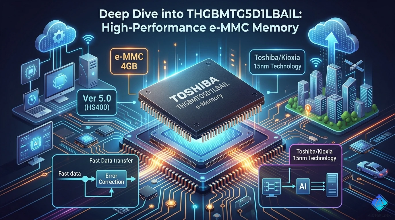
What Is THGBMTG5D1LBAIL? The One Character in Position 5 That Separates Three Generations of Kioxia 4GB eMMC
Here is a question that trips up engineers sourcing eMMC for embedded designs: what is the difference between THGBMDG5D1LBAIL, THGBMNG5D1LBAIL, and THGBMTG5D1LBAIL? All three are from Toshiba Memory Corporation (now Kioxia). All three are 4GB eMMC 5.0. All three ship in the same 153-ball WFBGA package, 11.5 mm × 13 mm. All three run from 3.3V VCC, operate from −25°C to +85°C, and achieve the same headline read speed of 152 MB/s in HS400 mode.
The difference is in position 5 of the part number: D, N, or T. That single character encodes the NAND flash process generation inside the package — which affects the NAND die's write endurance, erase speed, data retention characteristics, and the specific internal error correction workload the embedded controller must handle. From the host's perspective, all three are functionally interchangeable. From a reliability-and-longevity perspective, they are not the same component, and choosing between them (or confirming you received the generation you specified) requires understanding what that one character means.
1.0 Full Part Number Decoded: Every Field in THGBMTG5D1LBAIL
Toshiba (now Kioxia) NAND part numbers encode a complete product specification in a consistent positional system. THGBMTG5D1LBAIL breaks down as follows:
T — Manufacturer prefix: T = Toshiba (now Kioxia, but the T prefix is retained in product numbers)
H — Product category: H = NAND Flash memory product
G — Package type: G = BGA (Ball Grid Array)
B — Product type: B = eMMC module with integrated controller (as opposed to raw NAND)
M — Interface type: M = MMC/eMMC interface. This single letter distinguishes the entire eMMC family from raw NAND (N), USB (U), and eSD (S) variants in the same package families.
T — NAND generation / process node — the critical character:
- D = 19nm planar NAND (older generation, higher P/E cycle endurance per bit due to larger feature size, but lower bit density)
- N = 15nm planar NAND (Toshiba's 15nm generation, improved density vs D, slightly reduced raw endurance compensated by controller ECC)
- T = 15nm planar NAND — revised/improved version (Kioxia's refinement of the N-generation node; THGBMTG5D1LBAIL uses this die, same node designation as N but with process improvements)
- H = Higher-density / newer generation (used in extended-capacity and newer parts)
The D/N/T distinction is the key differentiator between generations of otherwise identical-looking 4GB eMMC parts from this manufacturer.
G — Density prefix: G = Gigabit range
5 — Density code: 5 = 32 Gbits per die = 4 GB total user capacity
D — Number of stacked NAND dies: D = 1 die (single die, no stacking). A "2" here would indicate two dies stacked in the package.
1 — Internal die configuration / spare area ratio subcode
L — Temperature grade:
- L = Standard commercial/industrial: −25°C to +85°C ambient
- H = Extended: −40°C to +105°C ambient (for automotive and harsh-environment variants)
B — Voltage configuration:
- B = VCC: 2.7V–3.6V (or 1.7V–1.95V); VCCQ: 1.7V–1.95V (or 2.7V–3.6V)
- More precisely for THGBMTG5D1LBAIL: VCC = 2.7–3.6V, VCCQ = 1.7–1.95V is the primary operating configuration
A — Package form: A = BGA (Ball Grid Array surface mount)
I — Package size code: I = 11.5 mm × 13 mm × 0.8 mm max height (153-ball WFBGA)
L — Package variant / generation marker: L = specific package iteration code for this product family
2.0 Specifications at a Glance
| Parameter | Value |
|---|---|
| Manufacturer | Kioxia (formerly Toshiba Memory Corporation) |
| User capacity | 4 GB |
| NAND type | 2D planar MLC (2-level cell) |
| NAND process node | 15 nm |
| eMMC standard | JEDEC/MMCA Version 5.0 |
| Interface modes | 1-bit, 4-bit, 8-bit MMC |
| High-speed mode | HS400 (requires 8-bit DDR at 200 MHz) |
| Sequential read (HS400) | Up to 152 MB/s |
| Sequential write (HS400) | Up to 14 MB/s |
| Package | 153-ball WFBGA (P-WFBGA153-1113-0.50) |
| Package dimensions | 11.5 mm × 13 mm × 0.8 mm max |
| Ball pitch | 0.50 mm |
| VCC (NAND/controller) | 2.7V – 3.6V |
| VCCQ (I/O) | 1.7V – 1.95V |
| Operating temperature | −25°C to +85°C (TA, standard grade) |
| Sleep mode current | ~100 µA typical |
| Integrated functions | ECC, wear leveling, bad block management |
| RoHS | Compliant |
3.0 The NAND Inside: What 15nm Means for System Reliability
The "T" in position 6 of THGBMTG5D1LBAIL identifies a 15nm process generation NAND die. Understanding what this means in practice requires separating two different effects of process node scaling.
What gets better as NAND process nodes shrink: Bit density increases — more storage capacity fits into the same silicon area, lowering cost per gigabyte. At 15nm, a single 32 Gbit (4 GB) die fits in a compact package. The 19nm (D-generation) die required slightly more silicon area for the same capacity.
What gets harder as NAND process nodes shrink: Individual flash cells store less charge, making each cell more sensitive to read disturb (the effect of reading one cell perturbing the charge in adjacent cells), retention degradation (charge loss over time without power), and program/erase endurance (the number of write-erase cycles a cell can sustain before the dielectric wears out). Smaller cells also require more powerful on-die ECC to achieve the same uncorrected bit error rate at a given P/E cycle count.
Practical implications for THGBMTG5D1LBAIL vs older D-generation: The 19nm D-generation eMMC (THGBMDG5D1LBAIL) uses larger cell geometry that offers somewhat more raw endurance per P/E cycle. The 15nm T-generation (THGBMTG5D1LBAIL) compensates with improved on-chip error correction and refined controller firmware. For typical embedded applications (device firmware storage, OS boot, application data) with moderate write frequency, the endurance of 15nm eMMC is entirely adequate. High-write-frequency applications (continuous logging, frequent large write operations) benefit from careful wear-leveling strategy and potentially specifying the extended-temperature H-grade or higher-endurance industrial eMMC variants.
THGBM (2D NAND) vs THGAM (3D NAND/BiCS): Kioxia's newer THGAM product family uses 3D BiCS FLASH™ (Bit Column Stacked) technology, where memory cells are stacked vertically rather than laid out in a single planar layer. The THGAM family delivers higher capacity per die, improved endurance relative to the planar 15nm generation, and is the current-generation choice for higher-capacity eMMC. THGBMTG5D1LBAIL is a 2D (planar) NAND part and is the appropriate choice for 4GB designs that have been validated against the THGBM electrical and timing characteristics. New designs where capacity requirements exceed 8GB should evaluate the THGAM family.
4.0 Four Misconceptions About This Part
Misconception 1: "All 4GB eMMC 5.0 in 153-ball WFBGA are interchangeable"
Electrically and from an eMMC interface protocol perspective, THGBMDG5D1LBAIL, THGBMNG5D1LBAIL, and THGBMTG5D1LBAIL are all pin-compatible in the 11.5 × 13 mm 153-ball package, and any compliant eMMC 5.0 host will communicate with all three identically. However, the internal NAND die is different, which means the internal controller firmware, the erase timing, the performance at varying temperatures, and the long-term retention behavior differ between generations. A supplier that ships THGBMDG5D1LBAIL (19nm die) when THGBMTG5D1LBAIL (15nm die) was specified has delivered a different internal component, even if immediate functional testing passes. If the process node matters for your reliability documentation or customer qualification, specify the exact part number and verify via CID (Card Identification) register reading.
Misconception 2: "The eMMC write speed spec (14 MB/s) is the bottleneck for all writes"
Sequential write speed in HS400 mode is specified at up to 14 MB/s for THGBMTG5D1LBAIL. This figure reflects sequential large-block writes, which are the most efficient writes for NAND flash. In practice, small random writes — the kind that operating systems and file systems generate constantly — are substantially slower and bounded by internal NAND program time and the controller's write buffering implementation. For OS boot storage on embedded Linux, the limiting performance metric for most user-visible operations is 4K random write IOPS, not sequential write speed. Always measure your application's actual I/O pattern against an eMMC rather than extrapolating from the sequential speed specification alone.
Misconception 3: "VCC and VCCQ can be powered from the same 3.3V rail"
THGBMTG5D1LBAIL specifies VCC at 2.7–3.6V and VCCQ at 1.7–1.95V. These are different voltage domains and cannot share a single 3.3V supply without a regulator. VCCQ is the I/O signaling voltage — it must match the host controller's I/O voltage to prevent signal integrity problems and potential damage to the eMMC I/O driver circuits. For HS400 operation, the host I/O voltage must be 1.8V (VCCQ = 1.8V). Supplying 3.3V to VCCQ while the host drives 1.8V signals will cause incorrect logic levels at the eMMC input; driving 3.3V I/O into a 1.8V VCCQ eMMC may damage the interface. Two separate, regulated supply rails are required.
Misconception 4: "Kioxia THGBMTG5D1LBAIL is a Toshiba part and Toshiba still makes it"
Toshiba Memory Corporation was established as a separate entity in 2017 when Toshiba Corporation spun off its memory business, and it was renamed Kioxia Corporation in 2019. The part number prefix THG (Toshiba NAND flash G-series) is retained in Kioxia's product numbering system for continuity. THGBMTG5D1LBAIL is a Kioxia product, manufactured under Kioxia's quality and supply chain systems, not Toshiba Corporation. When ordering, the manufacturer name to specify is Kioxia (or Kioxia America, Inc. for North American procurement). Distributors listing this part under "Toshiba" are using an outdated name; the manufacturer of record is Kioxia.
5.0 Host Interface Design and Integration Notes
Power supply — two rails required:
Supply VCC (2.7–3.6V, typically 3.3V) to the eMMC's NAND flash and controller core. Supply VCCQ (1.7–1.95V, typically 1.8V) to the I/O interface circuitry. Separate the two supplies with appropriately rated LDO regulators or dedicated DC-DC converters with adequate bypass:
- VCC: 10 µF bulk + 100 nF local ceramic at each VCC ball
- VCCQ: 1–4.7 µF bulk + 100 nF local ceramic at each VCCQ ball
- A bulk decoupling capacitor (22–47 µF, 6.3V rated X5R ceramic) at the VCC supply entry point to the PCB is strongly recommended — the eMMC controller generates significant current transients during internal NAND program and erase operations
Signal integrity for HS400 operation:
HS400 mode requires 8-bit DDR signaling at 200 MHz source-synchronous clock. Key PCB requirements:
- Data strobe (DS) pin must be routed with tight length matching to DAT0–DAT7 (within ±10 mil is typical)
- CMD and CLK traces: 50 Ω single-ended, 75–100 Ω for differential pairs where applicable
- Series resistors (22–33 Ω) on CMD, CLK, and DAT0–7 signals at the host side for impedance matching and overshoot damping
- Maximum trace length: 50 mm recommended for HS400; beyond this, simulation-verified tuning is necessary
Reset and initialization:
The RST_n pin is an active-low hardware reset input. On power-up, assert RST_n low for at least 1 µs, then release it. After RST_n de-assertion, the eMMC requires a minimum initialization period (governed by the CMD1/SEND_OP_COND handshake) before the host can access the device. Standard Linux kernel MMC drivers handle this automatically; bare-metal embedded firmware must implement the JEDEC eMMC initialization sequence.
NC and RFU pins:
The 153-ball package includes NC (No Connect), RFU (Reserved for Future Use), and VSF (Vendor Specific Function) balls. NC balls may be connected to ground or left floating. RFU balls must be left floating. VSF balls must be left floating unless vendor-specific functionality is intentionally accessed. Misconnecting RFU or VSF balls to VCC or GND can cause the device to enter an undefined state or fail to initialize.
6.0 Practice: Decoding Other THGBM Part Numbers
Once you understand the positional system, decoding any THGBM eMMC part number takes less than a minute.
Worked example 1: THGBMNG5D1LBAIL
| Position | Character | Meaning |
|---|---|---|
| 1–5 | THGBM | Toshiba/Kioxia eMMC module |
| 6 | N | 15nm NAND, N-generation (earlier than T) |
| 7 | G | Gigabit density range |
| 8 | 5 | 32 Gbit = 4 GB |
| 9 | D | Single NAND die |
| 10 | 1 | Die configuration code |
| 11 | L | Standard temp: −25°C to +85°C |
| 12 | B | VCC 3.3V, VCCQ 1.8V |
| 13 | A | BGA package |
| 14 | I | 11.5 × 13 × 0.8 mm |
| 15 | L | Package variant code |
→ THGBMNG5D1LBAIL = 4GB eMMC 5.0, 15nm N-generation NAND, standard temp, 153-ball WFBGA
Worked example 2: THGBMDG5D2HBAIL
Position 6 = D → 19nm NAND, older generation. Position 9 = 2 → two NAND dies stacked (2 × 32 Gbit = 8 GB... but wait — G5 = 32 Gbit is 4 GB per die, but with 2 stacked dies, capacity doubles). Position 11 = H → extended temperature, −40°C to +105°C.
→ THGBMDG5D2HBAIL = 8GB eMMC, 19nm NAND, 2 dies stacked, extended industrial temperature
Confirming: G5 (32 Gbit/die) × D2 (2 dies) = 64 Gbit total = 8 GB user capacity.
7.0 Real Questions from Embedded Engineers
Q: How do I verify the NAND generation (D vs N vs T) of an eMMC module I received, without physically opening the package?
A: Read the CID (Card Identification) register via the MMC interface. On Linux, this is accessible at /sys/class/mmc_host/mmc0/mmc0:0001/cid after the eMMC is initialized. The CID contains the manufacturer ID (MID), product name, product revision, product serial number, and manufacturing date. The MID for Kioxia is 0x11. The product name field contains an ASCII string that corresponds to the part number family. Cross-reference against Kioxia's CID documentation to confirm the specific die generation. Alternatively, the CSD (Card Specific Data) register contains the device specification version and speed grade information. On a properly functioning system, mmc extcsd read /dev/mmcblk0 (using the mmc-utils package) reads the extended CSD and provides detailed device information including firmware version, which can be correlated against Kioxia's firmware changelog for the specific die generation.
Q: My embedded Linux system boots from THGBMTG5D1LBAIL and the eMMC sometimes fails fsck with a corrupted superblock after unexpected power loss. Is this a hardware defect?
A: Probably not a hardware defect — this is a common outcome of unexpected power loss during a write operation without power loss protection (PLP) infrastructure. Standard eMMC 5.0 includes basic write buffering, and if power is removed while the internal NAND program operation is in progress (not yet completed), the partially written data can corrupt the block. For embedded Linux with journaling filesystems (ext4, f2fs), enable the filesystem's journal and ensure the journal is on the eMMC itself. The more robust solution is to use the eMMC's Enhanced Write Reliability (EWR) or Full Power Loss Protection if the specific device supports those features — check the extended CSD registers. For truly power-loss-safe designs, use the eMMC's cache flush command (CMD6 to flush the write cache) before initiating operations that require power-safe completion, and consider transitioning to an eMMC with explicit PLP certification.
Q: The datasheet for THGBMTG5D1LBAIL shows maximum write speed of 14 MB/s. But a Raspberry Pi CM4 with a 32GB eMMC achieves well above 40 MB/s write speed. Why?
A: The 14 MB/s specification is for THGBMTG5D1LBAIL specifically — a 4GB, single-die, 15nm planar NAND part. The CM4's 32GB eMMC uses a much newer Kioxia device from the THGAM family (3D BiCS NAND) with significantly higher write performance. More importantly, larger-capacity eMMC devices with multiple NAND dies can interleave write operations across dies, effectively multiplying the write bandwidth by the number of parallel die planes. A 4GB single-die eMMC has only one NAND die to write to at any given time; a 32GB multi-die eMMC can pipeline operations across 4 or more dies simultaneously. The 14 MB/s figure is accurate for this specific part in sequential write conditions. Comparing it to a fundamentally different capacity/generation part is an apples-to-oranges comparison.
8.0 Quick Reference Card
Part Number Positional Decode:
| Position | Characters | Field | THGBMTG5D1LBAIL Value |
|---|---|---|---|
| 1–4 | THGB | Toshiba/Kioxia BGA NAND | Fixed prefix |
| 5 | M | Interface type | M = eMMC |
| 6 | T | NAND generation | T = 15nm (improved) |
| 7 | G | Density range | G = Gigabit |
| 8 | 5 | Die capacity | 5 = 32 Gbit = 4 GB |
| 9 | D | Die stack count | D = 1 die |
| 10 | 1 | Configuration code | 1 |
| 11 | L | Temperature grade | L = −25°C to +85°C |
| 12 | B | Voltage config | B = VCC 3.3V, VCCQ 1.8V |
| 13 | A | Package family | A = BGA |
| 14 | I | Package size | I = 11.5×13×0.8mm |
| 15 | L | Package variant | L |
Generation Comparison — Position 6:
| Char | Generation | Node | Notes |
|---|---|---|---|
| D | Older | 19nm planar | Higher raw endurance/cell, lower bit density |
| N | Mid | 15nm planar | Standard Toshiba-era 15nm |
| T | Current | 15nm (improved) | Kioxia refinement of N-gen |
| H | Newer | Varies | Higher density variants |
Power Rails — Two separate supplies required:
| Rail | Voltage | Function |
|---|---|---|
| VCC | 2.7–3.6V (typically 3.3V) | NAND flash + controller core |
| VCCQ | 1.7–1.95V (typically 1.8V) | I/O signaling (must match host) |
Key Performance (HS400 mode):
- Sequential read: 152 MB/s max
- Sequential write: 14 MB/s max (single-die; interleaving not available)
On-chip functions: ECC, wear leveling, bad block management, write buffering
Linux verification: cat /sys/class/mmc_host/mmc0/mmc0:0001/cid to read CID register; Kioxia MID = 0x11
For sourcing Kioxia THGBMTG5D1LBAIL with verified authenticity and competitive pricing, visit aichiplink.com.

Written by Jack Elliott from AIChipLink.
AIChipLink, one of the fastest-growing global independent electronic components distributors in the world, offers millions of products from thousands of manufacturers, and many of our in-stock parts is available to ship same day.
We mainly source and distribute integrated circuit (IC) products of brands such as Broadcom, Microchip, Texas Instruments, Infineon, NXP, Analog Devices, Qualcomm, Intel, etc., which are widely used in communication & network, telecom, industrial control, new energy and automotive electronics.
Empowered by AI, Linked to the Future. Get started on AIChipLink and submit your RFQ online today!
Frequently Asked Questions
What is THGBMTG5D1LBAIL used for?
THGBMTG5D1LBAIL is a 4GB embedded MultiMediaCard (eMMC) storage device commonly used in embedded systems such as industrial controllers, IoT devices, and consumer electronics, where it provides non-volatile storage for operating systems, firmware, and application data with integrated features like wear leveling and error correction.
What does the “T” in THGBMTG5D1LBAIL indicate?
The “T” in the part number identifies the NAND generation, specifically an improved 15nm planar NAND process from Kioxia, which offers better density and controller-optimized reliability compared to older 19nm (D) and earlier 15nm (N) generations.
Is THGBMTG5D1LBAIL compatible with other THGBM eMMC parts?
Yes, it is generally pin-compatible and functionally interchangeable with other THGBM-series 4GB eMMC devices (like D or N variants) at the interface level, but differences in NAND generation can affect endurance, retention, and long-term reliability, which matters for qualified or industrial designs.
Why are two power supplies (VCC and VCCQ) required?
The device uses separate voltage domains—VCC (typically 3.3V) for the NAND and controller core, and VCCQ (typically 1.8V) for I/O signaling—to ensure proper signal integrity and compatibility with the host processor, especially for high-speed modes like HS400.
What limits the write performance of THGBMTG5D1LBAIL?
The relatively low write speed (around 14 MB/s) is mainly due to its single-die 4GB architecture and planar NAND limitations, meaning it lacks parallelism found in higher-capacity, multi-die eMMC devices, which can achieve much higher throughput through interleaving.


