Introduction
Every embedded system needs non-volatile memory — storage that retains its content when power is removed. Flash memory dominates this role across virtually every electronics segment, from the smallest IoT sensor node running on a coin cell to the most demanding industrial gateway running embedded Linux. Yet the term "flash memory" covers a broad family of technologies with fundamentally different architectures, performance characteristics, pin counts, reliability profiles, and cost points.
Choosing the wrong type can have serious consequences: a microcontroller that boots from the wrong flash type may miss its boot time target by an order of magnitude; a product built with too few P/E (program/erase) cycles will fail in the field before its design life; a storage solution without adequate ECC will corrupt data in a high-temperature industrial environment. Getting the decision right at the architecture stage saves enormous amounts of rework later.
This guide walks through every major flash memory technology available to embedded designers — NOR, NAND, SPI flash, eMMC, and UFS — with clear comparisons, practical selection criteria, and a step-by-step checklist. By the end, you will know exactly which type of flash belongs in your design and why.
1.0 Flash Memory Fundamentals: How It Works
1.1 How a Flash Memory Cell Stores Data
Flash memory stores data using floating-gate transistors — a standard MOSFET transistor modified with a second, electrically isolated gate (the "floating gate") sandwiched between the control gate and the channel. The floating gate is surrounded by thin oxide layers and has no direct electrical connection to any circuit.
Data is stored by trapping electrons on the floating gate:
- Logic "1" (erased state): No electrons on the floating gate. The transistor turns on normally at the standard threshold voltage.
- Logic "0" (programmed state): Electrons are injected onto the floating gate using Fowler-Nordheim tunneling or hot-carrier injection, raising the transistor's threshold voltage. The transistor no longer turns on at the standard voltage, representing a "0."
Reading a cell applies a sense voltage between the two threshold voltages and detects whether the transistor conducts — determining which state the cell is in. Writing (programming) adds electrons; erasing removes them by applying a large reverse voltage that pulls electrons back through the oxide via Fowler-Nordheim tunneling.
This process of physically moving electrons through oxide is what gives flash memory its non-volatility — the trapped charge persists for years without power — and also what limits its endurance, since the oxide degrades slightly each time electrons tunnel through it.
1.2 The Erase-Before-Write Constraint
The most important behavioral characteristic of flash memory — one that every embedded system designer must internalize — is the erase-before-write constraint:
- Flash cells can be programmed (written from 1 to 0) one bit at a time or in small groups (pages).
- Flash cells cannot be directly reprogrammed from 0 back to 1 — they must first be erased.
- Erasure happens in blocks — sections much larger than a single page, typically 4 KB to 256 KB depending on the flash type. The entire block must be erased as a unit.
This means: if you need to change one byte in a 64 KB block, you must read the entire block into RAM, modify your byte in RAM, erase the entire 64 KB block, and rewrite the entire block back to flash. This read-modify-erase-write cycle is the fundamental overhead of all flash write operations and is the primary reason flash memory requires careful software management.
The implications for system design are significant: flash memory is not a drop-in replacement for RAM. It requires a file system or firmware update mechanism specifically designed around the block-erase constraint. For raw NAND flash, this means implementing (or using a library with) a Flash Translation Layer (FTL). For NOR flash, it means structuring your data in fixed-size sectors aligned to erase boundaries. For eMMC and UFS, the integrated controller handles this transparently — but at the cost of non-deterministic latency during garbage collection.
1.3 XIP (Execute in Place) and Why It Matters for Boot
XIP (Execute in Place) is the ability of a processor to execute code directly from flash memory without first copying it to RAM. NOR flash supports XIP because its architecture allows random byte-level read access to any address in the flash — the processor can fetch instructions from flash as if it were ROM.
NAND flash, by contrast, uses a page-serial access architecture — data must be read in complete pages (typically 512 B to 16 KB) and cannot be addressed byte-by-byte in a memory-mapped fashion. NAND flash does not support XIP.
XIP has major implications for system cost and PCB complexity. If a processor runs XIP directly on NOR Flash using, for example, x8 Octal SPI Flash, the number of pins is significantly reduced compared to a store-and-download scheme using eMMC for storage and LPDDR2 RAM for code execution, resulting in savings of up to 2 to 4 layers of PCB design and lower overall system cost.
For MCU-based systems (without a separate DRAM), NOR flash is often the only practical non-volatile code storage solution because the MCU may lack the RAM needed to copy code from NAND flash before execution.
1.4 Flash and OTA Firmware Updates
Over-the-Air (OTA) firmware updates are a standard requirement for virtually every connected embedded product today — IoT sensors, industrial gateways, consumer appliances, and medical devices all require the ability to update firmware in the field without physical access.
Flash memory design for OTA must address three requirements:
Dual-bank (A/B) partitioning: The flash is divided into two equal firmware partitions (A and B). The device boots from A, downloads the new firmware to B, verifies its integrity, then switches the boot pointer to B. If the new firmware fails, the device falls back to A. This requires enough flash density to hold two complete firmware images simultaneously — a key sizing input.
Atomic write and integrity verification: Each firmware page must be written with a CRC or hash, and the overall image must be verified before the boot pointer is switched. The erase-before-write constraint means an interrupted OTA update (from a power outage, for example) must leave the device in a recoverable state — the old partition must remain intact until the new one is fully verified.
Endurance budget: OTA updates add to the flash write cycle count. A device that updates firmware weekly for a five-year service life accumulates 260 complete flash write cycles on top of normal runtime writes. This must be included in the endurance calculation.
2.0 NOR Flash vs. NAND Flash: Architecture, Performance & Use Cases
2.1 NOR Flash: Fast Read, Low Density, True XIP
NOR flash is the technology choice for code storage, boot firmware, and applications requiring fast, random read access. Its defining characteristics:
- Architecture: Each cell connects directly between a bit line and ground with its own NOR gate configuration — any bit can be read individually via a unique address
- Read speed: Extremely fast random reads — typical SPI NOR at 133 MHz QSPI achieves 66 MB/s sequential read; typical random access latency is 30–100 ns for parallel NOR
- Write/erase speed: Slow — page program time is typically 0.5–2 ms; sector (4 KB) erase takes 60–150 ms; bulk (full chip) erase can take 15–60 seconds
- Density range: 512 Kb to 2 Gb (64 MB) for most production parts; up to 8 Gb in stacked configurations
- Endurance: Typically 100,000 P/E cycles (some automotive-grade NOR devices achieve over 1 million cycles)
- Interface options: SPI (4-wire), Dual SPI (6-wire), Quad SPI (QSPI, 6-wire), Octal SPI (OPI, 11-wire), parallel (x8/x16, 48+ pins)
- XIP support: Yes — full byte-level random read access; processor can fetch code directly
- ECC requirement: Not required for standard use (NOR has very low raw bit error rates); some automotive-grade devices include optional ECC for safety-critical applications
When to choose NOR flash:
- MCU-based designs where code executes directly from flash (XIP)
- Boot firmware storage in systems with NAND or eMMC for bulk data (NOR holds the first-stage bootloader)
- Configuration parameter and calibration data storage
- Safety-critical applications (automotive, medical, industrial) where reliability and deterministic read latency are paramount
- Systems requiring fast boot time — NOR flash starts providing valid data in nanoseconds; no initialization or ECC correction required
Leading NOR flash families: Winbond W25Q series (SPI NOR, 512 Kb–2 Gb), Micron MT25Q series (Octal SPI NOR), Infineon/Cypress S25FL and S28HS series (HyperBus/OctalSPI), Macronix MX25L/MX25R series (low-power SPI NOR), ISSI IS25LP/IS25WP series.
2.2 NAND Flash: High Density, Lower Cost, Needs ECC
NAND flash is the technology choice for bulk data storage, media files, OS root filesystems, and any application requiring gigabytes of storage at the lowest cost per bit. Its defining characteristics:
- Architecture: Cells are connected in series strings (the NAND configuration), sharing bit lines — individual bytes cannot be addressed directly; access is page-serial
- Read speed: Fast sequential reads — typical SPI NAND reads at 80–100 MB/s; raw parallel NAND can achieve 200–400 MB/s with ONFI 4.0 interface
- Write/erase speed: Much faster than NOR — page program time is typically 200–500 µs; block (128 KB–2 MB) erase takes 2–10 ms
- Density range: 1 Gb to 512 Gb and beyond for a single die; multi-die packages reach 1 Tb+
- Endurance: Varies significantly by cell type (see Section 4.1); SLC NAND: 100,000+ P/E cycles; MLC: 3,000–10,000 cycles; TLC: 1,000–3,000 cycles
- Interface options: SPI NAND (4/6-wire), raw parallel NAND (ONFI, JEDEC Toggle, x8/x16, 48 pins)
- XIP support: No — page-serial architecture does not support byte-level random access
- ECC requirement: Mandatory — NAND has significantly higher raw bit error rates than NOR, requiring error correction codes (ECC) with typically 4–16 bits of correction per 512-byte sector; bad block management is also required
When to choose raw NAND flash:
- High-density storage needs (1 GB and above) where eMMC overhead or cost is not justified
- Designs where the host processor already includes a dedicated NAND controller (many application processors have integrated NAND flash controllers with hardware ECC)
- Cost-optimized designs willing to implement FTL and ECC in software
- Industrial and automotive applications where the designer needs direct control over wear leveling and reliability management
SPI NAND: A growing category of NAND with an SPI-compatible serial interface (versus traditional parallel NAND). SPI NAND retains NAND's high density at lower pin count (similar to SPI NOR), but requires ECC and bad block management and cannot support XIP. Popular in IoT and industrial gateway designs where parallel NAND's pin count is prohibitive but eMMC's footprint is too large.
2.3 SPI (Serial) Flash vs. Parallel Flash: Interface Trade-Offs
The choice between serial (SPI) and parallel flash interfaces has significant implications for PCB design, firmware complexity, and achievable performance:
SPI (Serial Peripheral Interface) Flash: Standard SPI NOR uses 4 pins (CLK, CS, MOSI, MISO). Quad SPI (QSPI) uses 6 pins (CLK, CS, IO0–IO3). Octal SPI uses 11 pins. At 133 MHz QSPI, peak read bandwidth is 66 MB/s — adequate for most embedded Linux boot and code storage applications. Benefits: minimal PCB routing, standard interface supported by virtually every MCU and processor, works on 2-layer PCBs.
Parallel Flash: Parallel NOR with x8 data bus and 24-bit address requires up to 47 total pins. The benefit is maximum random read bandwidth — parallel NOR at 133 MHz x16 can deliver over 200 MB/s. However, up to 47 pins are needed for NOR flash memory with up to 24 pins for address and 16 pins for data, making parallel flash impractical for compact designs and requiring more PCB layers for routing. Parallel flash is largely reserved for high-performance MCU designs where QSPI bandwidth is insufficient for real-time code execution demands.
2.4 NOR vs. NAND: Complete Comparison Table
| Parameter | SPI NOR Flash | Parallel NOR Flash | SPI NAND Flash | Raw Parallel NAND |
|---|---|---|---|---|
| Cell architecture | NOR (random access) | NOR (random access) | NAND (page serial) | NAND (page serial) |
| Typical density | 512 Kb – 2 Gb | 128 Mb – 2 Gb | 1 Gb – 8 Gb | 1 Gb – 512 Gb |
| Cost per bit | High | High | Medium | Low |
| Read speed | 66 MB/s (QSPI) | >200 MB/s | 80 MB/s | 200–400 MB/s |
| Write speed | Slow (0.5–2 ms/page) | Slow | Fast (200–500 µs/page) | Fast |
| Erase unit | Sector (4 KB) / Block | Sector / Block | Block (128 KB) | Block (128 KB–2 MB) |
| XIP support | Yes | Yes | No | No |
| ECC required | No | No | Yes | Yes |
| Bad block mgmt | No | No | Yes | Yes |
| Pin count | 4–11 pins | 34–47 pins | 4–6 pins | 48 pins |
| Endurance (SLC) | 100,000 cycles | 100,000 cycles | 100,000 cycles | 100,000 cycles |
| Endurance (MLC/TLC) | N/A | N/A | 3,000–10,000 cycles | 1,000–10,000 cycles |
| Typical application | MCU firmware, boot code | High-speed XIP | IoT data storage | Mass storage, OS |
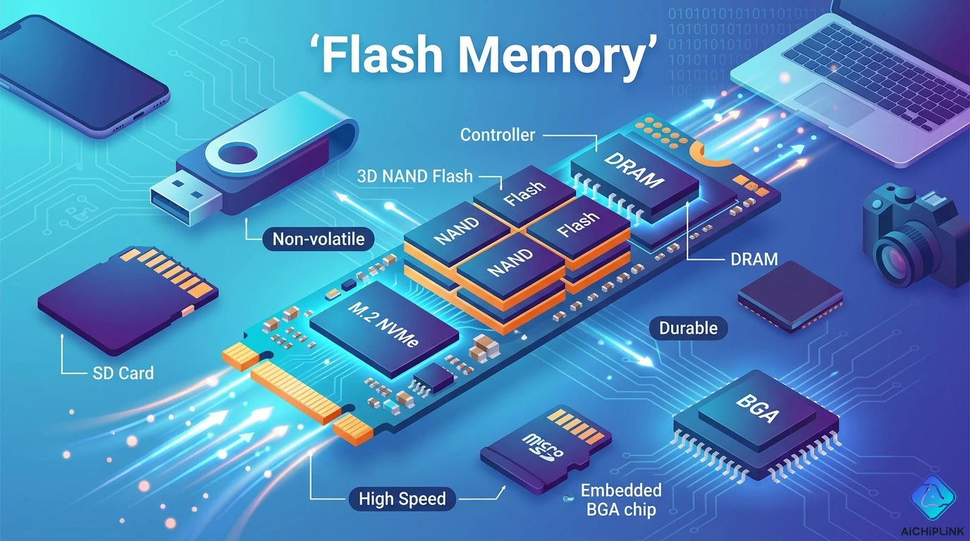
3.0 Managed NAND: eMMC, UFS, and SD Cards
3.1 eMMC: The Workhorse of Embedded Linux Storage
eMMC (embedded MultiMedia Card) is a NAND flash die packaged together with a proprietary NAND flash controller, all in a single BGA package. The controller handles ECC, bad block management, wear leveling, and the Flash Translation Layer (FTL) — presenting a simple, standardized block-device interface to the host processor.
From the system designer's perspective, eMMC behaves like a small hard drive: the host sends read/write commands via the MMC/SD protocol, and the controller handles all the flash management complexity internally. This dramatically reduces firmware development effort compared to raw NAND.
Key eMMC characteristics:
- Interface: 8-bit parallel MMC protocol, up to 400 MB/s (eMMC 5.1 HS400 mode); 10 signal pins total
- Density range: 4 GB to 256 GB per package
- Performance: eMMC 5.1 achieves up to 400 MB/s sequential read, 150–200 MB/s sequential write, ~10,000 IOPS random 4K read
- Reliability features: Integrated ECC, bad block management, wear leveling, write cache with power-loss protection (on industrial-grade variants)
- Power consumption: ~0.5 W during read/write; low-power states available
- Package: Standard 153-ball VFBGA (11.5 × 13 mm) or 100-ball LBGA
- Operating temperature: Commercial (0°C to +70°C) or industrial (−40°C to +85°C)
eMMC devices are "managed NAND" chips that provide data handling and wear management functions, including ECC and bad block management, that simplify embedded design significantly.
When to choose eMMC:
- Embedded Linux systems (the eMMC is the dominant storage medium for Linux-based embedded platforms)
- Designs where the host processor does not include a raw NAND controller
- Applications needing 4 GB+ storage with a simple, proven interface
- Products where development time and firmware complexity must be minimized
Leading eMMC suppliers: Samsung (KLMAG), Micron (MTFC), Kingston (EMMC08G), SK Hynix (H26M), Western Digital (SDINDDH4), Toshiba/Kioxia (THGBMNG).
3.2 UFS: High-Speed Managed Flash for Mobile and Demanding Embedded
UFS (Universal Flash Storage) is the successor to eMMC in high-performance mobile and embedded platforms. Where eMMC uses a parallel interface (8-bit data bus), UFS uses a serial M-PHY + UniPro protocol stack — the same physical layer used in MIPI mobile interfaces — enabling dramatically higher performance:
- UFS 2.1: ~1,200 MB/s sequential read, ~500 MB/s sequential write
- UFS 3.1: ~2,100 MB/s sequential read, ~1,200 MB/s sequential write
- UFS 4.0: ~4,200 MB/s sequential read, ~2,800 MB/s sequential write
UFS also supports command queue (hardware-level I/O reordering) and a half-duplex to full-duplex upgrade path, unlike eMMC's half-duplex-only architecture.
The trade-off versus eMMC is interface complexity: UFS requires dedicated M-PHY lanes (typically 2 lanes × differential pair = 4 data signal pins + additional control signals), and the host processor must include a UFS host controller — not all embedded processors support UFS. eMMC is universally supported by MCUs and application processors; UFS is primarily found in flagship mobile SoCs (Qualcomm Snapdragon, Samsung Exynos, MediaTek Dimensity).
When to choose UFS:
- Flagship smartphone, tablet, or high-performance embedded platform
- Applications requiring > 1 GB/s storage throughput (4K video editing, AI inference with large models, real-time data acquisition)
- Designs where the SoC supports UFS and eMMC's 400 MB/s ceiling is a bottleneck
3.3 eMMC vs. UFS vs. Raw NAND vs. SPI NOR: Selection Matrix
| Factor | SPI NOR Flash | SPI NAND Flash | Raw Parallel NAND | eMMC | UFS |
|---|---|---|---|---|---|
| Max density | 2 Gb (256 MB) | 8 Gb (1 GB) | 512 Gb (64 GB) per die | 256 GB | 1 TB+ |
| Interface pins | 4–6 | 4–6 | 48 | 10 | 6–8 |
| Seq. read BW | 66 MB/s | 80 MB/s | 400 MB/s | 400 MB/s | 4,200 MB/s |
| XIP support | Yes | No | No | No | No |
| ECC / FTL managed | No (not needed) | Requires host ECC | Requires host FTL | Yes (internal) | Yes (internal) |
| OS required | No | No | Optional | Optional | Optional |
| Endurance (typical) | 100K cycles | 100K (SLC) | 1K–100K cycles | Managed by controller | Managed by controller |
| Power (active) | Low | Low | Medium | ~0.5 W | ~0.8 W |
| Relative cost | High/MB | Medium/MB | Low/MB | Low-medium/GB | Medium/GB |
| Primary use case | MCU boot / config | IoT data log | Linux root FS | Embedded Linux | High-perf mobile/embedded |
4.0 Endurance, Reliability & Selection Criteria
4.1 Cell Types: SLC, MLC, TLC, QLC — Endurance vs. Density Trade-Off
Flash memory cells can store different numbers of bits per cell, trading endurance for density:
SLC (Single-Level Cell) — 1 bit per cell:
- P/E cycle endurance: 100,000+ cycles (some industrial SLC: 1 million cycles)
- Read latency: ~25 µs
- Data retention: 10+ years at 85°C
- Cost: Highest per GB
- Use cases: Automotive, industrial, aerospace — wherever longevity and reliability are paramount
MLC (Multi-Level Cell) — 2 bits per cell:
- P/E cycle endurance: 3,000–10,000 cycles
- Read latency: ~50 µs
- Data retention: 5–10 years at 85°C
- Cost: Medium
- Use cases: Consumer and mid-range industrial applications; balance of density and reliability
TLC (Triple-Level Cell) — 3 bits per cell:
- P/E cycle endurance: 1,000–3,000 cycles
- Read latency: ~100 µs (4× slower than SLC for random reads)
- Data retention: 1–5 years at 85°C (varies significantly with P/E cycle count)
- Cost: Low; dominant in consumer SSDs, smartphones, eMMC
- Use cases: Consumer electronics, high-capacity embedded storage where write frequency is low
QLC (Quad-Level Cell) — 4 bits per cell:
- P/E cycle endurance: 100–1,000 cycles
- Read latency: Higher than TLC
- Cost: Lowest per GB
- Use cases: Read-intensive bulk storage only; not appropriate for write-heavy embedded applications
The general rule: as the number of bits per cell increases, performance and life of NAND flash may degrade, increasing random read times to 100 µs for TLC NAND — four times the time required in SLC NAND and twice the time required in MLC NAND.
4.2 Calculating Flash Memory Lifetime for Your Application
Before committing to a flash type, calculate whether it will survive your design's write demands over its intended service life. The formula:
Lifetime (years) = (Flash_Capacity × P/E_Cycles) / (Daily_Write_Bytes × 365 × WAF)
where WAF (Write Amplification Factor) accounts for the overhead of erase-before-write cycles — typically 1.5–3× for managed NAND (eMMC, UFS) and up to 10× for poorly managed raw NAND with large erase blocks.
Example calculation: An IoT device logs 100 KB of sensor data per day to a 4 GB eMMC (TLC NAND, 1,000 P/E cycles, WAF = 2):
Lifetime = (4 × 10⁹ bytes × 1,000) / (100 × 10³ bytes × 365 × 2) = 4 × 10¹² / 7.3 × 10⁷ = 54,795 years
This example shows that a low-write IoT sensor logger is essentially immune to NAND wear. Now consider a data-intensive industrial controller that writes 100 MB/day to the same device:
Lifetime = (4 × 10⁹ × 1,000) / (100 × 10⁶ × 365 × 2) = 4 × 10¹² / 7.3 × 10¹⁰ = 54.8 years
Still comfortable. But if the same system writes 10 GB/day (common in high-frequency logging or video recording):
Lifetime = (4 × 10⁹ × 1,000) / (10 × 10⁹ × 365 × 2) = 4 × 10¹² / 7.3 × 10¹² = 0.55 years
This system would wear out in six months — catastrophic for a product with a five-year design life. The solution: increase flash density (larger eMMC), upgrade to SLC NAND for critical partitions, reduce write frequency via RAM buffering, or implement wear leveling more aggressively.
4.3 Automotive and Industrial Grade Flash: AEC-Q100 and Extended Temperature
Standard commercial-grade flash memory is qualified for 0°C to +70°C. Automotive and industrial deployments routinely see temperatures from −40°C to +125°C, plus vibration, humidity, and 15+ year service life requirements. Choosing standard commercial flash for these environments risks premature failure.
Automotive and industrial applications require flash devices to operate reliably for more than 15 years and maintain stored data integrity. Typically, SLC NAND and MLC NAND have worse bit error rates than NOR devices, and bit errors may occur in writing to the memory array or from electron leakage caused by read disturbs or other factors.
Key requirements for automotive and industrial flash:
- AEC-Q100 Grade 1 (−40°C to +125°C) or Grade 0 (−40°C to +150°C) qualification for automotive applications
- Extended temperature (−40°C to +85°C) for industrial grade
- JEDEC-standard reliability qualifications: HTOL (High Temperature Operating Life), HTSL (High Temperature Storage Life), Thermal Cycling, ESD/Latch-up
- Long lifecycle commitment: Automotive components require 10–15 year supply availability; confirm with the manufacturer that the specific part has a long-lifecycle guarantee
- Data retention at temperature: NOR flash typically specifies 20-year retention at 85°C; verify the data retention specification matches your worst-case operating temperature
Leading automotive/industrial flash suppliers: Infineon/Cypress (Semper NOR Flash, industrial NAND), Micron (automotive-qualified NAND and NOR), Winbond (industrial series W25Q-IQ suffix), Renesas/Dialog, and Macronix industrial series.
4.4 Seven-Step Flash Memory Selection Checklist
Use this checklist in order for every new design:
Step 1 — Quantify storage capacity: How many megabytes (or gigabytes) of non-volatile storage does your application require? < 64 MB favors NOR; 64 MB–1 GB opens both NOR and NAND/eMMC; > 1 GB strongly favors NAND, eMMC, or UFS.
Step 2 — XIP requirement: Does your processor execute code directly from flash (XIP), or does it copy code to RAM before execution? If XIP is required (most MCU designs), you must use NOR flash. If a load-to-RAM architecture is acceptable (most Linux-based designs), NAND/eMMC/UFS are options.
Step 3 — Interface constraint: How many GPIO/signal pins can you dedicate to flash? SPI (4–6 pins) is the universal constraint-satisfier. If you need > 66 MB/s bandwidth, consider QSPI or eMMC. If you need > 400 MB/s, consider UFS.
Step 4 — Calculate endurance: Using the formula in Section 4.2, calculate the expected flash lifetime under your worst-case write scenario. If TLC NAND meets the requirement with margin, no upgrade is needed. If not, step up to MLC or SLC.
Step 5 — Temperature and reliability grade: What are the minimum and maximum operating temperatures? −40°C to +85°C requires industrial grade. −40°C to +125°C requires automotive (AEC-Q100 Grade 1). Confirm the temperature grade is available in the flash family you have selected.
Step 6 — ECC and bad block management: If using raw NAND or SPI NAND, confirm your host processor or firmware implements ECC and bad block management. If not, switch to eMMC or UFS where the controller handles this internally.
Step 7 — Verify supply longevity: For industrial and automotive designs, confirm the selected flash part has a minimum 10-year supply guarantee from the manufacturer or distributor. Flash memory product lifecycles can be short — selecting a commodity part with no longevity commitment risks mid-production obsolescence.
5.0 Where to Source Flash Memory Components
Flash memory ICs are stocked in volume by all major authorized distributors. When sourcing for production designs, prioritize parts from authorized channels (DigiKey, Mouser, Arrow, Avnet, LCSC) to guarantee genuine parts with manufacturer traceability — counterfeit flash memory is a real risk in the secondary market, with counterfeit parts often exhibiting incorrect capacity, poor data retention, and early failure.
Key manufacturers and their flagship product families: Winbond (W25Q SPI NOR, W25N SPI NAND), Micron (MT25Q/N NOR, raw NAND, eMMC), Samsung (K9/K3 NAND, eMMC, UFS), Kioxia/Toshiba (NAND, eMMC), SK Hynix (NAND, eMMC, UFS), Infineon/Cypress (Semper NOR, SLC NAND), Macronix (MX25 SPI NOR), and ISSI (IS25LP SPI NOR).
For a broad selection of NOR, NAND, eMMC, and SPI flash memory ICs with verified authenticity, competitive pricing, and volume procurement support, visit aichiplink.com.
6.0 Conclusion
Choosing the right flash memory technology is one of the most consequential decisions in embedded system design. The wrong choice — a NOR flash that cannot hold the Linux filesystem, a TLC eMMC that wears out in two years under a high-write workload, or a raw NAND device without adequate ECC support — can require a full hardware redesign or cause field failures that damage product reputation and customer trust.
The decision framework is systematic. Start with capacity: if you need gigabytes, NAND-based solutions (raw NAND, eMMC, or UFS) are the only realistic options; if you need megabytes for firmware and configuration, NOR flash is the natural fit. Layer in the XIP requirement: if the processor executes code directly from flash (typical for MCU designs), NOR is mandatory. Then consider interface constraints (pin count, PCB complexity), calculate endurance against your worst-case write scenario, verify the temperature and reliability grade matches your operating environment, and confirm supply longevity from the manufacturer.
For the majority of embedded Linux designs, eMMC is the practical workhorse — managed NAND with an integrated controller, 4–256 GB density, 400 MB/s throughput, and a simple 10-pin interface that every processor supports. For MCU-based designs with code storage requirements up to 256 MB, SPI NOR flash is the universal solution — simple, reliable, XIP-capable, and available in 4–6 pin packages from dozens of manufacturers. For the most demanding performance applications with UFS-capable processors, UFS 3.1/4.0 delivers storage performance that rivals desktop SSDs in an embedded package.
For sourcing NOR flash, NAND flash, eMMC, and all other flash memory components with verified authenticity and competitive pricing, explore the full range available at aichiplink.com.

Written by Jack Elliott from AIChipLink.
AIChipLink, one of the fastest-growing global independent electronic components distributors in the world, offers millions of products from thousands of manufacturers, and many of our in-stock parts is available to ship same day.
We mainly source and distribute integrated circuit (IC) products of brands such as Broadcom, Microchip, Texas Instruments, Infineon, NXP, Analog Devices, Qualcomm, Intel, etc., which are widely used in communication & network, telecom, industrial control, new energy and automotive electronics.
Empowered by AI, Linked to the Future. Get started on AIChipLink.com and submit your RFQ online today!
Frequently Asked Questions
Can I use SPI NOR flash for an embedded Linux system?
SPI NOR flash can be used for embedded Linux, but it is generally not ideal for full systems due to its limited density (typically ≤256 MB) and slow write/erase performance. While it can support lightweight distributions like OpenWrt or uClinux in highly constrained designs, most Linux systems require larger storage (50–200 MB+ root filesystem) and frequent writes. In practice, SPI NOR is best used for bootloader storage, paired with NAND or eMMC for the main OS and data.
What is the difference between SLC and MLC NAND in eMMC?
The main difference is endurance and reliability: SLC NAND offers much higher durability (10,000–100,000 P/E cycles) and better performance, while MLC/TLC NAND provides higher density at lower cost. Consumer eMMC typically uses TLC for affordability, whereas industrial eMMC uses SLC or pSLC for long lifespan, data retention, and operation across wide temperature ranges (−40°C to +85°C), making it more suitable for mission-critical and embedded applications.
Does eMMC need ECC, and does the designer have to implement it?
Yes, eMMC requires ECC, but it is handled internally by the device, so the designer does not need to implement it. Unlike raw NAND, eMMC integrates a controller that automatically performs error correction, wear leveling, and bad block management. This allows the host system to interact with eMMC as a simple block storage device, significantly reducing software complexity and development effort.
What is XIP and which flash types support it?
XIP (Execute in Place) allows a processor to run code directly from flash memory without copying it to RAM, and it is supported only by NOR flash due to its byte-addressable random access. NAND flash, eMMC, and UFS do not support XIP because they rely on block/page-based access, requiring code to be loaded into RAM first. XIP is especially important in MCU-based systems with limited RAM, where it eliminates the need for external memory.
How do I choose between eMMC and UFS for a new embedded Linux platform?
The choice between eMMC and UFS depends on processor support and performance requirements. UFS offers much higher throughput (up to ~4200 MB/s) and is ideal for high-performance applications like 4K video, AI workloads, and fast data processing, but requires a compatible host controller. eMMC, with speeds up to ~400 MB/s, is more widely supported, lower cost, and sufficient for most embedded Linux systems, making it the practical default unless high bandwidth is essential.


