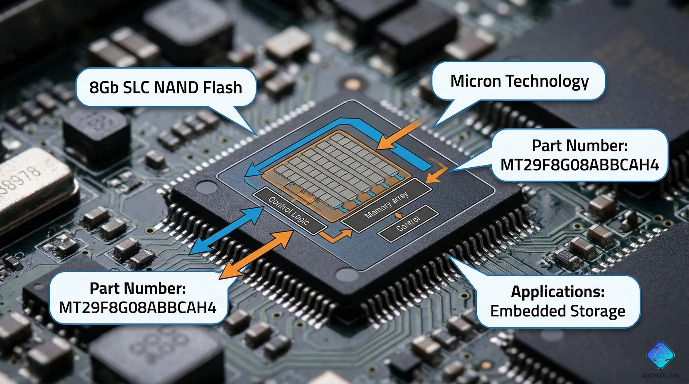
Product Quick Card
╔══════════════════════════════════════════════════════╗
║ MT29F8G08ABBCAH4 - At a Glance                      ║
╠══════════════════════════════════════════════════════╣
║ Manufacturer:  Micron Technology                    ║
║ Type:          NAND Flash Memory                    ║
║ Capacity:      8Gb (1GB) = 1,073,741,824 bytes     ║
║ Technology:    SLC (Single-Level Cell)              ║
║ Interface:     Async NAND (8-bit bus)               ║
║ Page Size:     2048 + 64 bytes (spare)             ║
║ Block Size:    128K + 4K bytes                      ║
║ Package:       48-pin TSOP1 (12×20mm)               ║
║ Voltage:       3.3V (2.7V - 3.6V)                   ║
║ Endurance:     100,000 P/E cycles                   ║
║ Temperature:   -40°C to +85°C (industrial)          ║
║ Status:        Active (mature product)              ║
╚══════════════════════════════════════════════════════╝
One-Line Summary: MT29F8G08ABBCAH4 is a 1GB SLC NAND flash with high endurance (100K cycles) for industrial embedded systems requiring reliable non-volatile storage.
Part Number Decoder
M T 2 9 F 8 G 0 8 A B B C A H 4
│ │ │ │ │ │ │ │ │ │ │ │ │ │ │ └─ 4 = Speed grade/revision
│ │ │ │ │ │ │ │ │ │ │ │ │ │ └─── H = RoHS compliant, Halogen free
│ │ │ │ │ │ │ │ │ │ │ │ │ └───── A = Package variant
│ │ │ │ │ │ │ │ │ │ │ │ └─────── C = Temperature grade (Commercial/Industrial)
│ │ │ │ │ │ │ │ │ │ │ └───────── B = Voltage (3.3V)
│ │ │ │ │ │ │ │ │ │ └─────────── B = Block size variant
│ │ │ │ │ │ │ │ │ └───────────── A = Architecture variant
│ │ │ │ │ │ │ │ └─────────────── 08 = 8-bit bus width
│ │ │ │ │ │ │ └───────────────── 0 = Page size indicator
│ │ │ │ │ │ └─────────────────── G = Gigabits
│ │ │ │ │ └───────────────────── 8 = 8 Gigabits (8Gb = 1GB)
│ │ │ │ └─────────────────────── F = NAND Flash
│ │ │ └───────────────────────── 29 = NAND product family
│ │ └─────────────────────────── T = Technology
│ └───────────────────────────── M = Micron
└─────────────────────────────── (Company identifier)

Result: 8Gb (1GB) SLC NAND, 8-bit bus, 3.3V, Industrial temp
Capacity Calculation:
8 Gigabits ÷ 8 bits/byte = 1 Gigabyte
1,073,741,824 bytes = 1,024 MB
Memory Organization
Capacity Breakdown
Total Capacity: 8Gb (8,589,934,592 bits)

Organization:
┌─────────────────────────────────────┐
│ 4096 Blocks                         │
│  └─ Each block = 64 Pages           │
│      └─ Each page = 2048 bytes      │
│          + 64 bytes spare area      │
└─────────────────────────────────────┘

Detailed Math:
Pages:     4096 blocks × 64 pages/block = 262,144 pages
Main area: 262,144 pages × 2048 bytes = 536,870,912 bytes (512 MB user data)
Spare area: 262,144 pages × 64 bytes = 16,777,216 bytes (16 MB spare)
Total:     512 MB + 16 MB = 528 MB physical = 1GB (with bad block management)
Array Structure
Block Structure:
┌──────────────────┐
│ Page 0           │ ← 2048 + 64 bytes
│ Page 1           │
│ Page 2           │
│ ...              │
│ Page 63          │
└──────────────────┘
Total: 64 pages per block

Page Structure:
┌─────────────────────────────────────┐
│ Main Area (2048 bytes)              │ ← User data
├─────────────────────────────────────┤
│ Spare Area (64 bytes)               │ ← ECC, metadata
│  ├─ ECC bytes (typical: 24 bytes)  │
│  ├─ Bad block marker (2 bytes)     │
│  └─ User metadata (38 bytes)       │
└─────────────────────────────────────┘
Technical Specifications
Electrical Characteristics
Power Supply:
VCC (Core voltage):
- Nominal: 3.3V
- Range: 2.7V - 3.6V
- Current:
  * Read: 25 mA (typical)
  * Program: 30 mA (typical)
  * Erase: 30 mA (typical)
  * Standby: 100 µA (typical)
I/O Voltage:
VIH (Input HIGH): 0.7 × VCC (min)
VIL (Input LOW):  0.3 × VCC (max)
VOH (Output HIGH): 2.4V (min) @ IOH = -100µA
VOL (Output LOW):  0.4V (max) @ IOL = 2.1mA
Performance Specifications
Access Times:
tR (Page Read):        25 µs (typical), 50 µs (max)
tPROG (Page Program):  300 µs (typical), 700 µs (max)
tBERS (Block Erase):   2 ms (typical), 10 ms (max)

Sequential Read:       ~40 MB/s (theoretical)
Sequential Write:      ~7 MB/s (typical)
Random Read IOPS:      ~40,000 IOPS
Random Write IOPS:     ~3,000 IOPS
Endurance & Retention:
Program/Erase Cycles:  100,000 cycles (SLC)
Data Retention:        10 years @ 25°C
                       1 year @ 85°C

Note: SLC provides superior endurance vs MLC/TLC
Interface Timing
Asynchronous Mode (Standard):
Operating Modes:
- Mode 0: tRC = 50 ns (20 MHz)
- Mode 1: tRC = 30 ns (33 MHz)
- Mode 2: tRC = 25 ns (40 MHz)
- Mode 3: tRC = 20 ns (50 MHz)

Key Timing Parameters:
tRC (Read cycle):      25 ns (min, Mode 2)
tWC (Write cycle):     25 ns (min, Mode 2)
tREA (Output delay):   20 ns (max)
tWP (WE pulse width):  12 ns (min)
tRP (RE pulse width):  12 ns (min)
Pinout & Package
48-Pin TSOP1 Package
        Top View (48-pin TSOP1)

    Pin 1 ○ ┌─────────────┐
    Pin 2   │             │
    Pin 3   │             │
    ...     │   MT29F8    │ 12mm × 20mm
    Pin 22  │             │ 1.0mm thickness
    Pin 23  │             │
    Pin 24  └─────────────┘
          ○ ○ ○ ○ ... ○ ○
         Pin 25      Pin 48

Pin 1 marker: Dot or notch
Pin pitch: 0.5mm
Pin Assignment Table
| Pin # | Name | Type | Function |
|---|---|---|---|
| 1 | NC | - | No connect |
| 2-9 | I/O0-I/O7 | I/O | Data bus (8-bit) |
| 10 | NC | - | No connect |
| 11 | NC | - | No connect |
| 12 | GND | PWR | Ground |
| 13-17 | NC | - | No connect |
| 18 | R/B# | O | Ready/Busy (open drain) |
| 19-23 | NC | - | No connect |
| 24 | GND | PWR | Ground |
| 25-29 | NC | - | No connect |
| 30 | RE# | I | Read Enable |
| 31 | CE# | I | Chip Enable |
| 32 | NC | - | No connect |
| 33-36 | NC | - | No connect |
| 37 | VCC | PWR | Power supply |
| 38 | NC | - | No connect |
| 39 | WP# | I | Write Protect |
| 40 | NC | - | No connect |
| 41 | CLE | I | Command Latch Enable |
| 42 | ALE | I | Address Latch Enable |
| 43 | WE# | I | Write Enable |
| 44-47 | NC | - | No connect |
| 48 | VCC | PWR | Power supply |
Critical Signals:
Data Bus:    I/O[7:0] (Pins 2-9)
Control:     CE#, CLE, ALE, RE#, WE#, WP#
Status:      R/B# (Ready/Busy indicator)
Power:       VCC (Pins 37, 48), GND (Pins 12, 24)
Command Set
Basic NAND Commands
Command          Code    Description
──────────────────────────────────────────
Read Page        00h/30h Two-cycle command
Read ID          90h     Read device ID
Reset            FFh     Reset device
Page Program     80h/10h Two-cycle command
Block Erase      60h/D0h Two-cycle command
Read Status      70h     Check operation status
Command Sequences
Read Page Sequence:
1. CE# = LOW (select chip)
2. Send 00h (Read command 1st cycle)
3. Send column address (2 bytes)
4. Send row address (3 bytes)
5. Send 30h (Read command 2nd cycle)
6. Wait for R/B# = HIGH (ready)
7. Send 00h + column address (if needed)
8. Toggle RE# to read data
9. CE# = HIGH (deselect)

Total time: ~25-50 µs (page read time)
Page Program Sequence:
1. CE# = LOW
2. Send 80h (Program command 1st cycle)
3. Send column address (2 bytes)
4. Send row address (3 bytes)
5. Send data (2048 bytes + spare)
6. Send 10h (Program command 2nd cycle)
7. Wait for R/B# = HIGH
8. Read status (70h)
9. CE# = HIGH

Total time: ~300-700 µs (program time)
Block Erase Sequence:
1. CE# = LOW
2. Send 60h (Erase command 1st cycle)
3. Send row address (3 bytes, block address)
4. Send D0h (Erase command 2nd cycle)
5. Wait for R/B# = HIGH
6. Read status (70h)
7. CE# = HIGH

Total time: ~2-10 ms (erase time)
Status Register
Bit 7 6 5 4 3 2 1 0
    │ │ │ │ │ │ │ └─ FAIL (0=Pass, 1=Fail)
    │ │ │ │ │ │ └─── Reserved
    │ │ │ │ │ └───── Reserved
    │ │ │ │ └─────── Reserved
    │ │ │ └───────── Reserved
    │ │ └─────────── Write Protect (1=Protected)
    │ └───────────── Reserved
    └─────────────── Ready (0=Busy, 1=Ready)

Read after Program/Erase to check success:
Bit 0 = 0 → Operation successful ✅
Bit 0 = 1 → Operation failed ❌
Application Examples
Application 1: Embedded Linux Boot Storage
Use Case:
Embedded system with Linux kernel + root filesystem
MT29F8G08 stores:
- Bootloader (U-Boot): 1-2 MB
- Linux kernel: 4-8 MB
- Root filesystem: 200-500 MB
- Data partition: Remaining space
Partition Layout:
Block 0-7:     Bootloader (1 MB)
Block 8-71:    Linux kernel (8 MB)
Block 72-2119: Root FS (256 MB)
Block 2120-4095: User data (240 MB)

With bad block management:
Effective capacity: ~900 MB (10% reserved)
Application 2: Industrial Data Logger
Use Case:
Industrial sensor data logging device
Requirements:
- High endurance (100K cycles) ✅
- Temperature range (-40 to +85°C) ✅
- Reliable storage (SLC) ✅
- Non-volatile (NAND) ✅
Data Management:
Circular buffer implementation:
- Write to sequential blocks
- Erase oldest block when full
- Wear leveling across all blocks

Lifespan calculation:
100,000 cycles × 4096 blocks = 409.6 million writes
At 1000 writes/day: 1,122 years theoretical
Application 3: Firmware Storage (Field Updates)
Use Case:
Device firmware with over-the-air (OTA) updates

Dual-boot partition scheme:
Partition A (Active):   128 MB
Partition B (Standby):  128 MB
Data partition:         Remaining

Update process:
1. Download new firmware to Partition B
2. Verify integrity (checksum)
3. Switch boot flag
4. Reboot to Partition B
5. If successful, mark B as active
6. If failed, rollback to Partition A
Design Guidelines
Schematic Design
Power Supply Design:
VCC Filtering:
Source → [10µF tantalum] → VCC pins
         [0.1µF ceramic]  (near each VCC pin)

Minimum capacitors:
- 1× 10µF (bulk)
- 2× 0.1µF (one per VCC pin: pins 37, 48)

Place capacitors within 5mm of IC
Pull-up/Pull-down Resistors:
Required Pull-ups (to VCC):
- R/B# pin: 10kΩ (open-drain output)
- WP# pin: 10kΩ (if not actively driven)

Optional Pull-ups:
- CE#, RE#, WE#: 47kΩ (keep inactive when not driven)

Not required:
- I/O pins (tri-state with weak pull-up)
PCB Layout Guidelines
Trace Routing:
Data Bus (I/O[7:0]):
- Keep traces equal length (±1 mm)
- Width: 6-8 mil (0.15-0.2mm)
- Spacing: 6 mil minimum
- Avoid running parallel >10mm

Control Signals (CE#, WE#, RE#, etc.):
- Width: 6-8 mil
- Keep short and direct
- Avoid stubs

Power/Ground:
- VCC trace: 20 mil minimum width
- GND: Use plane if possible
- Star grounding for decoupling caps
Component Placement:
Priority:
1. Decoupling capacitors (closest to VCC pins)
2. Pull-up resistors (near R/B#, WP#)
3. Controller/processor interface

Thermal considerations:
- TSOP1 package has good thermal performance
- No special cooling required
- Ensure airflow in enclosed systems
Interface Design
Typical Controller Connection:
MCU/SoC                MT29F8G08ABBCAH4
GPIO[7:0] ←──────────→ I/O[7:0]
GPIO_CE   ────────────→ CE#
GPIO_CLE  ────────────→ CLE
GPIO_ALE  ────────────→ ALE
GPIO_WE   ────────────→ WE#
GPIO_RE   ────────────→ RE#
GPIO_WP   ────────────→ WP#
GPIO_RB   ←──────────── R/B#

8 data + 6 control = 14 GPIO minimum
Alternative: Use Dedicated NAND Controller:
Many SoCs include NAND controller:
- Hardware ECC generation
- DMA support for data transfer
- Automatic timing control
- Reduced CPU overhead

Examples:
- STM32F4/F7 (FMC with NAND support)
- i.MX6/7/8 (GPMI NAND controller)
- Allwinner A33/H3 (NAND controller)
ECC (Error Correction Code)
Why ECC is Essential
NAND Flash Bit Errors:
Causes:
- Read disturb (repeated reads to same block)
- Program disturb (adjacent page programming)
- Data retention over time
- Wear from P/E cycles

SLC NAND typical error rate:
- Fresh: 1 error per 10^17 bits (very rare)
- After 100K cycles: 1 error per 10^8 bits
- After 10 years: 1 error per 10^7 bits

ECC corrects these errors automatically
ECC Requirements
Recommended ECC Strength:
For MT29F8G08 (SLC NAND):
- Minimum: 1-bit ECC per 512 bytes
- Recommended: 4-bit ECC per 512 bytes
- Best practice: 8-bit ECC per 512 bytes

Page size: 2048 bytes = 4 sectors × 512 bytes
ECC overhead (4-bit per 512B):
  4 sectors × 7 bytes = 28 bytes
  Fits in 64-byte spare area ✅
ECC Algorithm Options:
Hamming Code:
- Simple, low overhead
- 1-bit correction per block
- Software implementation easy

BCH (Bose-Chaudhuri-Hocquenghem):
- Multi-bit correction (4/8/16-bit)
- Moderate complexity
- Hardware accelerators available

Reed-Solomon:
- Strong multi-bit correction
- Higher complexity
- Less common in NAND
Bad Block Management
Factory Bad Blocks
Specification:
Maximum bad blocks: 40 blocks (1% of 4096)
Location: Any block
Marking: First page, spare area byte 0 or 1
  Valid block: 0xFF
  Bad block:   ≠ 0xFF
Bad Block Detection:
At manufacturing:
1. Read page 0 spare area of each block
2. Check byte 0 and byte 1
3. If either ≠ 0xFF → Mark as bad
4. Create bad block table (BBT)

Software should:
- Scan all blocks on first use
- Maintain BBT in non-volatile memory
- Skip bad blocks during read/write
Runtime Bad Block Handling
Detecting New Bad Blocks:
During operation, monitor:
- Program failures (status bit 0 = 1)
- Erase failures (status bit 0 = 1)
- Excessive ECC corrections (>threshold)

When detected:
1. Mark block as bad in BBT
2. Relocate data to spare block
3. Update file system mapping
Bad Block Table (BBT) Structure:
Simple BBT (2 bits per block):
00 = Good block
01 = Reserved (wear leveling)
10 = Factory bad block
11 = Runtime bad block

Size: 4096 blocks × 2 bits = 1024 bytes (1 KB)
Store: In known-good block + backup copy
Wear Leveling
Why Wear Leveling Needed
Problem:
Without wear leveling:
Block 0:   100,000 writes → Worn out
Block 1:   100,000 writes → Worn out
Block 2:   5,000 writes → Still good
Block 3:   1,000 writes → Fresh

Result: Premature failure (only 2% used)
Solution: Distribute Writes Evenly
With wear leveling:
All blocks: ~50,000 writes average
Result: Maximize device lifespan
Wear Leveling Algorithms
Static Wear Leveling:
Periodically move static data to high-erase-count blocks
Move dynamic data to low-erase-count blocks

Example:
Block 100 (static, 100 erases):
  Move to Block 500 (10,000 erases)
Block 200 (dynamic, 15,000 erases):
  Move to Block 100 (now 101 erases)
Dynamic Wear Leveling:
Distribute new writes to low-erase-count blocks

Erase Count Table:
Block 0:  5,000 erases
Block 1:  12,000 erases
Block 2:  3,000 erases ← Choose this for next write
Block 3:  8,000 erases
File System Recommendations
Suitable File Systems
For Embedded Linux:
UBIFS (Unsorted Block Image File System):
✅ Designed for NAND flash
✅ Built-in wear leveling
✅ Bad block handling
✅ Compression support
✅ Fast mount time

JFFS2 (Journaling Flash File System 2):
✅ Robust journaling
✅ Wear leveling
⚠️ Slow mount on large flash
⚠️ High RAM usage

YAFFS2 (Yet Another Flash File System):
✅ Optimized for NAND
✅ Fast
⚠️ Not in mainline Linux kernel
Raw NAND vs Managed NAND
Raw NAND (MT29F8G08):
Pros:
✅ Lower cost per GB
✅ Full control over management
✅ Customizable algorithms

Cons:
❌ Requires ECC implementation
❌ Bad block management needed
❌ Wear leveling required
❌ More complex software
Managed NAND (eMMC alternative):
Pros:
✅ Built-in controller (FTL)
✅ ECC handled automatically
✅ Wear leveling built-in
✅ Simpler interface

Cons:
❌ Higher cost
❌ Less control
❌ Fixed performance characteristics
Troubleshooting Guide
Problem: Read Errors / Data Corruption
Checklist:
☐ Check ECC implementation (is it working?)
☐ Verify power supply stability (ripple <50mV)
☐ Check signal integrity (clean waveforms?)
☐ Review timing parameters (meeting specs?)
☐ Test with different NAND device (HW or chip fault?)
☐ Monitor temperature (within -40 to +85°C?)
☐ Check for worn blocks (exceeded P/E cycles?)
ECC Threshold Monitoring:
Track correctable errors:
0 corrections: Good ✅
1-2 corrections: Normal
3-4 corrections: Marginal ⚠️
>4 corrections: Block wearing out ❌

When >4: Mark block for retirement
Problem: Write/Erase Failures
Diagnostic Steps:
1. Read Status Register after operation
   Bit 0 = 1 → Failure

2. Retry operation (up to 3 times)
   If still fails → Block is bad

3. Mark block as bad in BBT

4. Relocate data to spare block

5. Update wear leveling map
Common Causes:
- Block exceeded endurance (>100K cycles)
- Voltage drop during write
- Timing violation
- Physical damage to die
Problem: Slow Performance
Performance Optimization:
1. Use Page-aligned access
   Misaligned: 3× slower
   Aligned: Full speed ✅

2. Batch operations
   Single page: 300 µs
   Sequential 64 pages: 300 µs + 63×25 µs = 1.8 ms
   → 64× faster throughput

3. Pipeline operations
   Program page N while reading page N+1
   Overlap operations for efficiency

4. Use hardware NAND controller if available
   DMA transfer: 10× faster than GPIO bit-banging
Alternative Parts & Cross-Reference
Direct Replacements (Pin-compatible)
Micron Family:
MT29F8G08ABACAH4: Same specs, different revision
MT29F8G08ADBDAH4: Enhanced version

Samsung:
K9F8G08U0M: Similar 8Gb SLC NAND
K9F8G08U0A: Older generation

Toshiba (Kioxia):
TC58NVG4S0F: 8Gb SLC
Capacity Variants (Same Family)
Lower capacity:
MT29F4G08ABBDAH4: 4Gb (512 MB)
MT29F2G08ABBDAH4: 2Gb (256 MB)

Higher capacity:
MT29F16G08ABACAH4: 16Gb (2 GB)
MT29F32G08ABACAH4: 32Gb (4 GB)

Note: Pinout may differ for higher densities
Summary & Quick Reference
Key Specifications Summary
Capacity:      1 GB (8 Gbit)
Technology:    SLC (high endurance)
Interface:     Async 8-bit parallel
Page:          2048 + 64 bytes
Block:         64 pages (128KB)
Endurance:     100,000 P/E cycles
Speed:         25 µs read, 300 µs write
Package:       48-pin TSOP1
Temperature:   -40 to +85°C
Voltage:       3.3V (2.7-3.6V)
Design Checklist
Hardware:
☑ VCC decoupling (10µF + 2× 0.1µF)
☑ R/B# pull-up (10kΩ)
☑ WP# pull-up (10kΩ if unused)
☑ Signal traces <10cm, controlled impedance
☑ Power supply stable (2.7-3.6V)

Software:
☑ ECC implemented (4-bit minimum)
☑ Bad block management
☑ Wear leveling algorithm
☑ Power-fail recovery
☑ Read retry on errors
☑ Block retirement strategy
Conclusion
The MT29F8G08ABBCAH4 is a reliable SLC NAND flash offering 1GB capacity with exceptional endurance (100,000 P/E cycles) for industrial embedded applications. Its 48-pin TSOP1 package and standard asynchronous interface make it suitable for systems requiring non-volatile storage with long lifespan and wide temperature operation.
Successful implementation requires:
- Proper ECC implementation (4-bit or higher)
- Comprehensive bad block management
- Effective wear leveling algorithms
- Robust power supply design
Compared to modern MLC/TLC NAND, SLC provides superior endurance and data retention, making it ideal for mission-critical industrial applications despite higher cost per gigabyte.
For detailed datasheets, application notes, and NAND flash design resources, visit AiChipLink.com.

Written by Jack Elliott from AIChipLink.
AIChipLink, one of the fastest-growing global independent electronic components distributors in the world, offers millions of products from thousands of manufacturers, and many of our in-stock parts is available to ship same day.
We mainly source and distribute integrated circuit (IC) products of brands such as Broadcom, Microchip, Texas Instruments, Infineon, NXP, Analog Devices, Qualcomm, Intel, etc., which are widely used in communication & network, telecom, industrial control, new energy and automotive electronics.
Empowered by AI, Linked to the Future. Get started on AIChipLink and submit your RFQ online today!
Frequently Asked Questions
What is MT29F8G08ABBCAH4 used for?
The MT29F8G08ABBCAH4 is mainly used in embedded systems such as industrial controllers, data loggers, and Linux-based devices, where reliable non-volatile storage and high endurance are required.
Is MT29F8G08ABBCAH4 SLC or MLC NAND?
This device uses SLC (Single-Level Cell) technology, which provides much higher endurance (up to 100,000 P/E cycles) and better data retention compared to MLC or TLC NAND, making it ideal for industrial applications.
Does MT29F8G08ABBCAH4 require ECC?
Yes, like all raw NAND flash, it requires external ECC (Error Correction Code); typically, a 4-bit or stronger ECC per 512 bytes is recommended to ensure data integrity over the device’s lifespan.
What interface does MT29F8G08ABBCAH4 use?
It uses a standard asynchronous 8-bit parallel NAND interface with control signals like CE#, CLE, ALE, WE#, and RE#, meaning it usually connects to an MCU or SoC with a NAND controller or GPIO-based interface.
What are the main alternatives to MT29F8G08ABBCAH4?
Common alternatives include parts from Micron Technology (same family revisions), as well as compatible devices from Samsung Electronics and Kioxia, offering similar 8Gb SLC NAND specifications.


