Here is a question the datasheets rarely answer clearly: if K3LKCKC0BM is described as a "64Gb" chip, why does every distributor listing call it an "8GB" or even a "64GB" memory chip? And why do some listings say it runs at 5500 MHz while Samsung's own specification says 6400 Mbps?
None of these descriptions are wrong. They are just measuring different things — and the confusion is a perfect illustration of how DRAM specifications work and why part numbers like K3LKCKC0BM look intimidating until you understand the naming logic behind them.
The short answer: K3LKCKC0BM is a Samsung LPDDR5 DRAM die, 64 Gigabits of memory (= 8 Gigabytes), organized as a dual-channel x32 interface, running at up to 6,400 Megabits per second per pin. It is a current-production mobile memory component used in smartphones, tablets, and AI edge devices — and it is distinctly different from the newer LPDDR5X family, a distinction that matters to system architects choosing memory for 5G and on-device AI applications.
This explainer decodes every field in the part number, walks through the arithmetic that converts Gigabits to Gigabytes, explains the LPDDR5 interface architecture, and clears up the misconceptions that cause the most confusion.
1.0 What Is K3LKCKC0BM? The One-Paragraph Answer
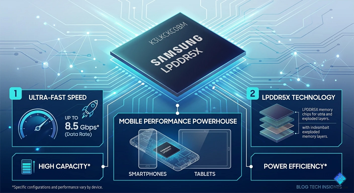
K3LKCKC0BM is a Samsung LPDDR5 SDRAM component — a single-package mobile DRAM die with 64 Gigabits (8 Gigabytes) of capacity, a dual-channel x32 data bus, and a maximum data rate of 6,400 Megabits per second per pin. It is packaged in Samsung's standard 315-ball FBGA (11.5 mm × 13 mm), the same footprint used across Samsung's LPDDR4, LPDDR5, and LPDDR5X families. It is fully compliant with the JEDEC LPDDR5 standard (JESD209-5) and supports LPDDR5's signature power-saving features: DVFS, DQ Copy, WriteX, and deep sleep modes. It is a currently active, mass-produced product in Samsung's lineup, used by SoC manufacturers including Qualcomm (Snapdragon) and MediaTek (Dimensity) platforms in flagship and near-flagship mobile devices.
2.0 Full Part Number Decoded: Every Character in K3LKCKC0BM-MGCP
Samsung's DRAM part numbers follow a consistent encoding logic. Here is the complete decode for K3LKCKC0BM-MGCP:
K — Samsung DRAM product category identifier (K = Samsung semiconductor memory)
3 — DRAM sub-category (3 = DRAM component, as opposed to modules or multichip packages)
L — Memory type (L = Low Power DDR, i.e., LPDDR family)
K — Generation / speed tier:
- K = LPDDR5 (this generation)
- KL = LPDDR5X (the next generation, as in K3KL9L90CM)
- Note this carefully: one extra letter distinguishes LPDDR5 from LPDDR5X in Samsung's naming
C — Die density code within the LPDDR5 generation (C = 64 Gb single die)
K — Organization / channel configuration (K = x32, dual-channel, 16-bit per channel)
C — Package die count / stacking (C = single die)
0 — Revision / variant indicator
BM — Package body size and type encoding (BM = specific FBGA dimensions)
— (hyphen) — separator between base part and ordering suffix
M — Package body size variant in the suffix
G — Temperature grade (G = commercial/mobile: −25°C to +85°C)
C — Packaging format (C = tray)
P — Speed bin / revision marker
Other suffix variants in this base family:
| Full Part Number | Temp Grade | Packaging | Notes |
|---|---|---|---|
| K3LKCKC0BM-MGCP | −25°C to +85°C | Tray | Standard production |
| K3LKCKC0BM-MFCP | −25°C to +85°C | Tray | Alternate speed/config bin |
| K3LKCKC0BM-MUCP | −25°C to +85°C | Tray | Another speed/config variant |
All three suffix variants share identical die density (64 Gb), organization (x32), and package (315-FBGA). The suffix letters after the hyphen refine speed bin, packaging format, and screening grade — but the core silicon is the same K3LKCKC0BM die.
3.0 The Math: How 64Gb Becomes 8GB and Why 5500 MHz Is Not the Same as 6400 Mbps
This is the section that resolves the confusion in every distributor listing.
Gigabits to Gigabytes:
When Samsung says the K3LKCKC0BM is "64 Gb," that 64 Gb refers to the total number of binary storage bits on the die — 64 × 10⁹ bits (approximately). Converting to bytes:
64 Gigabits ÷ 8 bits/byte = 8 Gigabytes
This is why the part number says "64 Gb" but every description says "8 GB." They are the same number expressed in different units. A chip that holds 64 Gb of data stores 8 GB — the full contents of a feature film, approximately 2,000 average-size photos, or a typical Android system partition plus a few applications.
The confusion multiplies because distributors sometimes write "64 GB" (with a capital B) instead of "64 Gb" (with a lowercase b), which would actually mean 64 Gigabytes — a completely different and much larger quantity. K3LKCKC0BM holds 8 GB, not 64 GB. Always check whether the B in a capacity spec is uppercase (bytes) or lowercase (bits).
5500 MHz vs 6400 Mbps — why both numbers appear:
LPDDR5 uses Double Data Rate (DDR) signaling — data is transferred on both the rising and falling edges of the clock. This means:
- If the clock runs at 3200 MHz, data transfers at 3200 × 2 = 6400 Mega-transfers per second = 6400 Mbps
- If the clock runs at 2750 MHz, data transfers at 2750 × 2 = 5500 Mbps
Some distributors and spec sheets report the clock frequency (2750 MHz or 3200 MHz), while others report the data rate (5500 Mbps or 6400 Mbps). Both can be correct for the same chip, depending on whether the SoC runs the LPDDR5 interface at maximum or a lower operating point.
Samsung's K3LKCKC0BM is rated for a maximum data rate of 6400 Mbps (at 3200 MHz clock). A listing that says "5500 MHz" is actually describing a data rate of 5500 Mbps (2750 MHz clock) — a valid lower operating point, but not the part's maximum rated speed.
Peak bandwidth calculation for a single K3LKCKC0BM:
The die has a x32 data bus (32 data pins). At 6400 Mbps:
Peak bandwidth = 6400 Mbps × 32 bits ÷ 8 bits/byte = 25.6 GB/s
For comparison, this is approximately the memory bandwidth of a high-end mobile SoC from the 2021–2022 era. Two dies in a package-on-package configuration would deliver 51.2 GB/s — which is exactly why Samsung's LPDDR5 marketing material highlights "51.2 GB/s" as the bandwidth headline for dual-die configurations.
4.0 LPDDR5 Architecture — What x32 Dual-Channel Actually Means
The K3LKCKC0BM presents two independent 16-bit channels to the host SoC — referred to as Channel A and Channel B. Each channel has its own:
- 16 data signals (DQ[0:15])
- 2 data strobe signals (DQS_t, DQS_c — differential pair)
- 1 data mask/inversion signal (DMI)
- Independent Command/Address (CA) bus
- Independent Chip Select (CS) control
Together, the two channels provide a 32-bit (x32) data path, which is why the part is described as "x32" in the organization field. The two channels can be operated simultaneously by the SoC memory controller for full 32-bit bandwidth, or independently for per-channel power management.
Why dual-channel matters for mobile AI:
Neural network inference workloads — the kind running in on-device AI applications on modern smartphones — are fundamentally memory-bandwidth-bound, not compute-bound. The model weights must be loaded from DRAM for every inference pass. A single-channel x16 LPDDR5 at 6400 Mbps delivers 12.8 GB/s. The dual-channel x32 K3LKCKC0BM delivers 25.6 GB/s from a single die — doubling the effective model loading rate and cutting inference latency roughly in half compared to a single-channel configuration of the same die.
Power management on the K3LKCKC0BM:
LPDDR5 introduced several power-reduction mechanisms over LPDDR4X:
DVFS (Dynamic Voltage and Frequency Scaling): The SoC can reduce both clock frequency and core supply voltage (VDD2) together during low-demand periods, reducing power consumption substantially. On the K3LKCKC0BM, VDD2H (1.05V) is used at full performance; VDD2L (0.9V) is used at lower frequencies.
DQ Copy: During read bursts, data from one DQ group can be copied to another instead of re-driving the I/O, saving switching energy on the data bus.
WriteX: Bundles write operations for improved bus utilization, reducing the number of command transactions needed for a given data transfer.
Deep Sleep / Power-Down: The device supports multiple low-power states including Deep Sleep (DSM) where only the self-refresh circuitry is active, reducing current draw to microampere levels while retaining stored data.
5.0 Where K3LKCKC0BM Is Used: Real Application Scenarios
The K3LKCKC0BM is designed for, and found in, the following application categories:
Flagship and near-flagship smartphones (2021–2023 generation): LPDDR5 at 6400 Mbps was the memory standard for Snapdragon 888, Snapdragon 8 Gen 1, and Dimensity 9000-class SoCs. Devices using these SoCs with 8GB of RAM configurations frequently use a single K3LKCKC0BM die. 12GB configurations stack one K3LKCKC0BM (8GB, 64 Gb) with one K3LKBKB0BM (4GB, 32 Gb) — both from the same Samsung LPDDR5 family.
High-performance tablets: Tablets prioritizing memory bandwidth for display rendering, video editing, and gaming use LPDDR5 in x32 configuration. The 25.6 GB/s single-die bandwidth of K3LKCKC0BM provides adequate throughput for 4K display pipelines.
Thin-and-light laptops with soldered LPDDR5: Notebook designs that solder LPDDR5 directly to the motherboard (rather than using SO-DIMM sockets) use this die family. Samsung's own LPCAMM2 memory modules for laptops use stacked versions of the same LPDDR5 die.
Automotive infotainment and ADAS (with grade qualification): The commercial-grade K3LKCKC0BM-MGCP is rated −25°C to +85°C. For automotive ADAS and infotainment applications requiring AEC-Q100, Samsung offers automotive-qualified LPDDR5 dies — a different part number suffix with extended qualification screening.
AI inference edge devices: Embedded Linux SBCs, edge AI accelerator boards, and IoT gateway platforms requiring high bandwidth memory in a space-constrained BGA form factor use LPDDR5 dies including K3LKCKC0BM. The low standby power of LPDDR5 is critical for battery-powered edge inference devices.
When NOT to specify K3LKCKC0BM:
- Maximum bandwidth applications (> 25.6 GB/s per die) → Use LPDDR5X (K3KL9L90CM-MGCT at 30 GB/s, or higher-density variants)
- Above +85°C operating temperature → Use Samsung's automotive LPDDR5 variants
- Systems with LPDDR4X-only memory controllers → LPDDR5 is not backward-compatible with LPDDR4X at the protocol level; verify SoC support
6.0 Five Misconceptions Engineers Have About This Part
Misconception 1: "K3LKCKC0BM is 64GB"
No. The die density is 64 Gb (Gigabits) = 8 GB (Gigabytes). The capital-B versus lowercase-b distinction matters enormously: 64 GB would be a 512-Gigabit die, which does not exist in any current LPDDR5 product. When a distributor listing says "64GB" for K3LKCKC0BM, they have made a unit error. The correct capacity is 8 GB per die.
Misconception 2: "LPDDR5 and LPDDR5X are the same — just a marketing name change"
They are related but distinct specifications. K3LKCKC0BM is LPDDR5, rated at 6400 Mbps maximum. The K3KL9L90CM is LPDDR5X, rated at 7500 Mbps maximum — a 17% speed increase. LPDDR5X also includes tighter AC timing margins, an enhanced DQ equalizer for ISI compensation at higher data rates, and additional power-saving modes. The physical package and pin assignments are compatible (same 315-FBGA footprint), but the SoC's memory controller must specifically support LPDDR5X speeds to use the LPDDR5X die at its maximum rate. An LPDDR5X die run at 6400 Mbps will work correctly, but you are paying for speed you are not using.
Misconception 3: "5500 MHz means this chip is slower than 6400 Mbps parts"
5500 MHz as listed by some distributors is actually the data rate in Megabits per second using non-standard notation — it should be written as 5500 Mbps, not 5500 MHz. This represents a lower operating point (2750 MHz clock × 2 for DDR = 5500 Mbps data rate) that the K3LKCKC0BM supports, not its maximum rated speed. The maximum rated data rate is 6400 Mbps. The listing using "5500 MHz" likely refers to a specific speed bin variant (the -MFCP suffix) qualified at the lower speed point.
Misconception 4: "The x32 means this is a 32-bit single-channel memory"
x32 refers to the total data bus width of the package (32 data pins), not the channel count. The K3LKCKC0BM implements this as two independent 16-bit channels (2 × x16), not a single 32-bit channel. This distinction matters because two independent channels allow the SoC to schedule reads and writes to each channel independently, improving effective bandwidth utilization versus a true single-channel 32-bit interface.
Misconception 5: "LPDDR5 can replace LPDDR4X in an existing design"
LPDDR5 is not electrically backward-compatible with LPDDR4X. The command and address bus architecture changed significantly between generations — LPDDR5 uses a 6-bit CA bus at DDR rate, while LPDDR4X uses a 10-bit CA bus. The power supply voltages are similar but not identical. A PCB designed for LPDDR4X will need signal routing changes, power supply adjustments, and a host SoC with a LPDDR5-capable memory controller to use K3LKCKC0BM. It is not a pin-compatible upgrade.
7.0 Real Questions About K3LKCKC0BM
Q: I see K3LKCKC0BM in a teardown photo of a 12GB RAM smartphone. But the die is only 8GB. How does the phone have 12GB?
A: Most likely the phone uses two LPDDR5 dies in a Package-on-Package (PoP) stack. A 12GB LPDDR5 configuration typically stacks one 64 Gb (8GB) die — likely K3LKCKC0BM — and one 32 Gb (4GB) die — likely K3LKBKB0BM. Both dies appear inside the same physical memory package that sits directly on top of the application processor in a PoP arrangement. From the outside it looks like one chip; internally it is two stacked DRAM dies. The SoC's memory controller addresses both dies across two separate CS (chip select) signals while sharing the same CA and DQ buses in a dual-die configuration.
Q: The K3LKCKC0BM is listed as LPDDR5 and the K3KL9L90CM is LPDDR5X. I need to design a new platform with 8GB RAM. Which should I specify?
A: For a new design starting in 2025 or later, specify K3KL9L90CM (LPDDR5X, 7500 Mbps) unless your SoC specifically does not support LPDDR5X speeds. LPDDR5X delivers 30 GB/s peak bandwidth versus 25.6 GB/s for LPDDR5 — a 17% bandwidth advantage that translates directly to better AI inference throughput and smoother 5G data processing. The PCB footprint is identical (both 315-FBGA). The price premium between LPDDR5 and LPDDR5X at equivalent density has narrowed as LPDDR5X has moved to volume production. If your SoC's maximum memory controller speed is 6400 Mbps, K3LKCKC0BM is fine — you would pay for LPDDR5X capability you cannot use.
Q: Can K3LKCKC0BM be used in an automotive ADAS system?
A: The standard K3LKCKC0BM-MGCP has a commercial temperature rating of −25°C to +85°C and is not AEC-Q100 qualified. For automotive ADAS applications requiring AEC-Q100, Samsung offers a dedicated automotive LPDDR5 product line with extended qualification and temperature rating up to +105°C. Contact Samsung Semiconductor directly or through an automotive-focused distributor to identify the correct part number for your temperature profile and qualification requirement.
Q: Samsung's product page shows "Sorry, no matches were found" when I search for K3LKCKC0BM. Does this mean it is discontinued?
A: No. This is a known display issue on Samsung Semiconductor's website where the product detail search returns a "no matches" message despite the product being actively listed on the same page. The K3LKCKC0BM is confirmed as a mass-production active product by multiple authorized distributors (with confirmed stock and datasheet availability). Samsung's FBGA Part Marking Decoder at semiconductor.samsung.com also correctly resolves K3LKCKC0BM. The web interface issue does not reflect product status — verify lifecycle through authorized distributors rather than the Samsung product page search.
8.0 Quick Reference Card
K3LKCKC0BM Decoded:
| Field | Character(s) | Meaning |
|---|---|---|
| Brand | K3 | Samsung DRAM |
| Type | L | LPDDR (Low Power DDR) |
| Generation | K | LPDDR5 (K = LPDDR5; KL = LPDDR5X) |
| Density | C | 64 Gb per die |
| Organization | K | x32 (dual 16-bit channel) |
| Package | C0BM | Single die, 315-FBGA |
| Temp grade (-MGCP) | G | −25°C to +85°C commercial |
The Unit Conversion Every Buyer Needs:
| What spec sheets say | What it means | Notes |
|---|---|---|
| 64 Gb | 8 GB capacity | Gigabits ÷ 8 = Gigabytes |
| 6400 Mbps | Max data rate | 3200 MHz clock × 2 (DDR) |
| 5500 Mbps | Lower operating point | 2750 MHz clock × 2 (valid but not max) |
| 25.6 GB/s | Peak bandwidth | 6400 Mbps × 32 bits ÷ 8 |
LPDDR5 (K3LKCKC0BM) vs LPDDR5X (K3KL9L90CM):
| Parameter | K3LKCKC0BM (LPDDR5) | K3KL9L90CM (LPDDR5X) |
|---|---|---|
| Max data rate | 6,400 Mbps | 7,500 Mbps |
| Peak BW (x32) | 25.6 GB/s | 30.0 GB/s |
| BW advantage | Reference | +17% |
| PCB footprint | 315-FBGA | 315-FBGA (same) |
| JEDEC standard | JESD209-5 | JESD209-5B |
| Best for | Proven SoCs, cost-conscious | New designs, AI/5G workloads |
Power Domains (same as LPDDR5X):
| Domain | Voltage | Function |
|---|---|---|
| VDD1 | 1.8V | I/O auxiliary |
| VDD2H | 1.05V | Core (high-performance) |
| VDD2L | 0.9V | Core (DVFS low-power) |
| VDDQ | 0.5V | DQ/DQS data I/O |
| VDDCA | 0.9V | Command/Address bus |
For verified authentic Samsung K3LKCKC0BM and related LPDDR5 memory components, visit aichiplink.com.

Written by Jack Elliott from AIChipLink.
AIChipLink, one of the fastest-growing global independent electronic components distributors in the world, offers millions of products from thousands of manufacturers, and many of our in-stock parts is available to ship same day.
We mainly source and distribute integrated circuit (IC) products of brands such as Broadcom, Microchip, Texas Instruments, Infineon, NXP, Analog Devices, Qualcomm, Intel, etc., which are widely used in communication & network, telecom, industrial control, new energy and automotive electronics.
Empowered by AI, Linked to the Future. Get started on AIChipLink.com and submit your RFQ online today!
Frequently Asked Questions
What is K3LKCKC0BM?
K3LKCKC0BM is a 64Gb (8GB) LPDDR5 mobile memory chip from Samsung Electronics, featuring a dual-channel x32 interface and speeds up to 6400 Mbps, widely used in smartphones and AI edge devices.
Is K3LKCKC0BM 64GB or 8GB?
K3LKCKC0BM is 8GB, not 64GB. The “64Gb” specification refers to Gigabits (Gb), and since 8 bits = 1 byte: 64Gb ÷ 8 = 8GB actual capacity. Listings showing “64GB” are incorrect unit conversions.
What is the bandwidth of K3LKCKC0BM?
K3LKCKC0BM delivers up to 25.6 GB/s bandwidth. Calculation: 6400 Mbps × 32-bit bus ÷ 8 = 25.6 GB/s, enabling high-speed data transfer for gaming, AI, and 5G applications.
What is the difference between LPDDR5 and LPDDR5X?
LPDDR5X is faster and more efficient than LPDDR5. LPDDR5 (K3LKCKC0BM): up to 6400 Mbps. LPDDR5X (e.g., K3KL9L90CM): up to 7500 Mbps. LPDDR5X provides ~17% higher bandwidth and improved signal integrity, making it better for modern flagship devices.
What does x32 dual-channel mean in K3LKCKC0BM?
x32 means a 32-bit total data bus, implemented as two independent 16-bit channels. This dual-channel design improves parallel data access, increasing real-world performance and efficiency compared to single-channel memory.


.png&w=256&q=75)