Introduction
Are you designing precision instrumentation, high-accuracy sensor interfaces, or critical analog signal conditioning circuits requiring ultra-low offset voltage and drift? The OPA2277UA represents Texas Instruments' proven solution for applications demanding exceptional DC precision, delivering industry-leading offset performance in a dual operational amplifier configuration optimized for precision measurement and instrumentation systems.
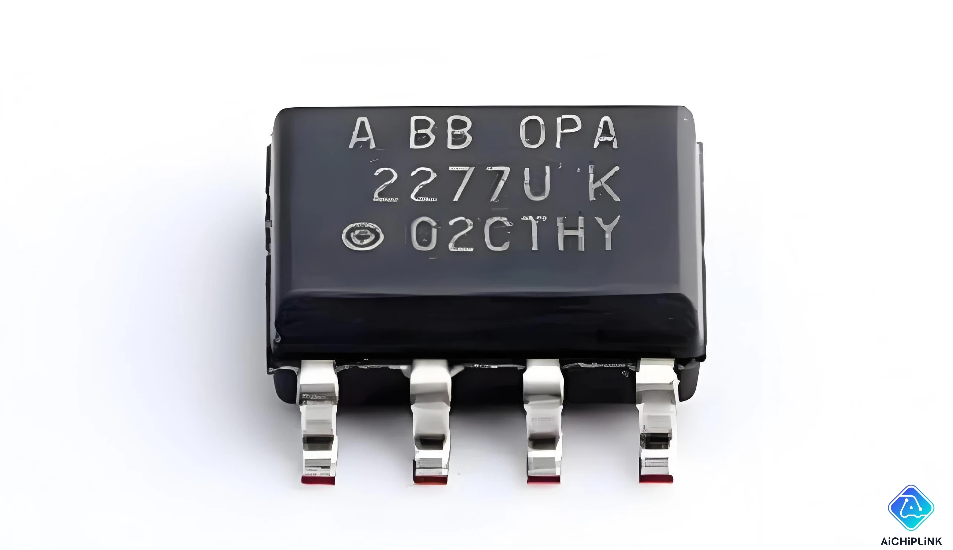
The OPA2277UA is a dual precision operational amplifier manufactured by Texas Instruments, a global leader in analog and mixed-signal semiconductors. This device features ultra-low offset voltage (10 μV typical), near-zero offset drift (0.1 μV/°C typical), and low noise performance in a space-efficient dual-amplifier package. Designed for applications where DC accuracy is paramount, it excels in precision instrumentation amplifiers, high-resolution data acquisition systems, strain gauge interfaces, thermocouple amplifiers, and critical sensor conditioning circuits requiring long-term stability and accuracy.
According to industry analysis, precision analog design continues to drive innovation in industrial automation, medical instrumentation, and scientific equipment where measurement accuracy directly impacts system performance and regulatory compliance. The OPA2277UA addresses these demands by providing laboratory-grade precision in production-ready integrated circuits, enabling engineers to achieve professional measurement accuracy without custom discrete designs or expensive chopper-stabilized amplifiers.
In this comprehensive technical guide, you'll discover the OPA2277UA's architecture, complete electrical specifications, performance analysis, proven application circuits, PCB design best practices, and competitive positioning to support informed component selection for precision analog designs requiring exceptional DC accuracy and long-term stability.
OPA2277UA Technical Overview
The OPA2277UA is a dual precision operational amplifier that combines ultra-low offset voltage with excellent drift characteristics in a standard 8-pin SOIC package, providing exceptional DC accuracy for critical measurement applications.
Core Specifications Summary
| Parameter | Specification | Significance |
|---|---|---|
| Configuration | Dual op-amp | Two amplifiers per package |
| Offset Voltage | 10 μV typ, 25 μV max | Ultra-low DC error |
| Offset Drift | 0.1 μV/°C typ | Excellent temperature stability |
| Input Bias Current | 0.2 nA typ | Minimal input loading |
| Voltage Noise | 0.35 μVp-p (0.1-10 Hz) | Low 1/f noise |
| CMRR | 120 dB typ | Excellent common-mode rejection |
| Gain Bandwidth | 1 MHz | Adequate for precision DC/low-frequency |
| Supply Voltage | ±2.5V to ±18V | Flexible power options |
| Package | SOIC-8 | Standard surface-mount |
Key Performance Advantages
Ultra-Low Offset Voltage:
- 10 μV typical (25 μV maximum)
- Enables high-accuracy measurements without trimming
- Critical for sensor interfaces and instrumentation
Exceptional Offset Drift:
- 0.1 μV/°C typical (0.2 μV/°C maximum)
- Maintains accuracy over temperature
- Reduces system calibration requirements
Low Input Bias Current:
- 0.2 nA typical (low temperature)
- Minimal error with high-impedance sources
- Ideal for sensor interfaces (thermocouples, RTDs)
Part Number Decoder
Understanding Texas Instruments nomenclature:
OPA2277UA breakdown:
- OPA = Operational amplifier
- 2 = Dual amplifier (two per package)
- 277 = Specific model series
- U = Package type (SOIC-8)
- A = Grade designation
Related Variants:
- OPA277 = Single amplifier version
- OPA2277P = DIP-8 package
- OPA2277UA/2K5 = Tape-and-reel packaging
Target Applications
The OPA2277UA excels in precision measurement applications:
Instrumentation:
- Precision instrumentation amplifiers
- Bridge amplifiers (Wheatstone, strain gauge)
- High-resolution data acquisition
- Test and measurement equipment
Sensor Interfaces:
- Thermocouple amplifiers
- RTD (Resistance Temperature Detector) interfaces
- Pressure sensor conditioning
- Load cell amplifiers
Industrial:
- Process control systems
- Factory automation sensors
- Precision current-to-voltage converters
- Reference voltage buffers
Medical:
- Biomedical instrumentation
- Patient monitoring equipment
- Laboratory analyzers
- Diagnostic equipment
Scientific:
- Laboratory instruments
- Precision measurement systems
- Chromatography equipment
- Spectroscopy systems
Precision Op-Amp Architecture
Understanding precision op-amp architecture reveals how the OPA2277UA achieves its exceptional DC performance through advanced design techniques.
Offset Voltage Sources and Reduction
Offset Voltage Origins:
In standard op-amps, offset voltage arises from:
- Input stage mismatch: Differential pair transistor variations
- Load mismatch: Unbalanced current mirror loading
- Packaging stress: Die attach and molding compound stress
OPA2277UA Offset Reduction Techniques:
┌──────────────────────────────────────────────┐
│    OPA2277UA Offset Reduction Architecture   │
├──────────────────────────────────────────────┤
│                                               │
│  ┌────────────────────────────────────────┐  │
│  │   Laser-Trimmed Input Stage            │  │
│  │   - Precision matching                 │  │
│  │   - Active trimming during mfg         │  │
│  │   → Achieves 10 μV typical offset      │  │
│  └────────────┬───────────────────────────┘  │
│               │                               │
│  ┌────────────▼───────────────────────────┐  │
│  │   Temperature Compensation             │  │
│  │   - Matched transistor pairs           │  │
│  │   - Thermal balancing                  │  │
│  │   → 0.1 μV/°C drift performance        │  │
│  └────────────┬───────────────────────────┘  │
│               │                               │
│  ┌────────────▼───────────────────────────┐  │
│  │   Low-Stress Packaging                 │  │
│  │   - Stress-relief die attach           │  │
│  │   - Controlled molding                 │  │
│  │   → Long-term offset stability         │  │
│  └────────────────────────────────────────┘  │
│                                               │
└──────────────────────────────────────────────┘
Laser Trimming:
- Factory trimming of on-chip resistors
- Nulls initial offset to 10 μV typical
- Permanent adjustment (not affected by temperature cycling)
Input Stage Design
Bipolar Input Transistors:
- PNP input pair for low input bias current
- Matched geometry for minimal offset
- Large emitter area for low noise
Benefits of Bipolar Design:
- Lower voltage noise than JFET (important for low-impedance sources)
- Lower offset than CMOS
- Stable over temperature
Internal Compensation
Frequency Compensation:
- Internally compensated for unity-gain stability
- 1 MHz gain-bandwidth product
- 45° phase margin (typical)
Trade-off:
- Lower bandwidth than general-purpose op-amps
- Optimized for DC and low-frequency precision
- Adequate for sensor interfaces (typically <10 kHz)
Common-Mode and Power Supply Rejection
CMRR (Common-Mode Rejection Ratio):
- 120 dB typical at DC
- Excellent rejection of common-mode noise
- Critical for instrumentation applications
PSRR (Power Supply Rejection Ratio):
- 120 dB typical at DC
- Minimizes power supply noise impact
- Enables use with less-regulated supplies
Complete Technical Specifications
Let's examine the detailed specifications defining the OPA2277UA's performance and operational parameters.
DC Electrical Specifications
| Parameter | Conditions | Typical | Maximum | Units |
|---|---|---|---|---|
| Offset Voltage (VOS) | TA = 25°C | 10 | 25 | μV |
| Offset Drift (ΔVOS/ΔT) | Full temperature | 0.1 | 0.2 | μV/°C |
| Input Bias Current (IB) | TA = 25°C | 0.2 | 2 | nA |
| Input Offset Current (IOS) | TA = 25°C | 0.1 | 1 | nA |
| Open-Loop Gain (AOL) | VO = ±10V, RL = 2kΩ | 120 | 110 | dB |
| CMRR | VCM = ±10V | 120 | 110 | dB |
| PSRR | VS = ±2.5V to ±18V | 120 | 110 | dB |
Key Specification Analysis:
Offset Voltage:
- 10 μV typical = 0.00001V error
- For 0-10V signal: 0.0001% error (1 ppm)
- Industry-leading for integrated op-amps
Offset Drift:
- 0.1 μV/°C × 50°C range = 5 μV total drift
- Maintains sub-10 μV accuracy over temperature
- Critical for outdoor/industrial applications
AC Specifications
| Parameter | Conditions | Typical | Units |
|---|---|---|---|
| Gain Bandwidth (GBW) | G = 1 | 1 | MHz |
| Slew Rate | VO = ±10V | 0.8 | V/μs |
| Settling Time | To 0.01%, 10V step | 15 | μs |
| Voltage Noise (0.1-10 Hz) | - | 0.35 | μVp-p |
| Voltage Noise Density | f = 10 Hz | 18 | nV/√Hz |
| Current Noise Density | f = 10 Hz | 0.2 | pA/√Hz |
AC Performance Notes:
Gain Bandwidth:
- 1 MHz suitable for DC to ~10 kHz signals
- Not for high-speed applications
- Optimized for precision, not speed
Noise Performance:
- 0.35 μVp-p (0.1-10 Hz): Excellent low-frequency noise
- 18 nV/√Hz @ 10 Hz: Low 1/f noise corner
- Suitable for precision measurements
Input/Output Specifications
| Parameter | Conditions | Typical | Units |
|---|---|---|---|
| Input Voltage Range | Linear operation | (VS-) - 1.5V to (VS+) - 2.5V | V |
| Common-Mode Range | CMRR > 100 dB | (VS-) to (VS+) - 2V | V |
| Output Swing | RL = 2kΩ | (VS-) + 0.5V to (VS+) - 0.5V | V |
| Output Current | Short circuit | ±25 | mA |
Operating Range:
- Supply voltage: ±2.5V to ±18V (flexible)
- Single supply: 5V to 36V (when configured for single supply)
- Input common-mode: Rail-to-rail minus ~2V headroom
Power Supply Specifications
| Parameter | Conditions | Typical | Maximum | Units |
|---|---|---|---|---|
| Supply Voltage | Dual supply | ±2.5 to ±18 | - | V |
| Supply Current (per amplifier) | Quiescent, no load | 1.8 | 2.5 | mA |
| Power Dissipation | TA = 25°C | - | 500 | mW |
Power Consumption:
- 3.6 mA typical for dual amplifier (1.8 mA × 2)
- Low power: Suitable for battery-powered applications
- 65 mW @ ±18V typical quiescent power
Temperature Specifications
| Parameter | Value | Units |
|---|---|---|
| Operating Temperature | -40 to +125 | °C |
| Storage Temperature | -65 to +150 | °C |
| Thermal Resistance (θJA) | 150 | °C/W |
Performance Characteristics
How does the OPA2277UA perform in real-world precision applications? Let's examine key performance aspects and design considerations.
Offset Voltage Performance
Statistical Distribution:
For a typical production lot:
- Mean offset: ~10 μV
- Standard deviation: ~5 μV
- 99% within: ±20 μV
- Maximum spec: 25 μV (guaranteed)
Temperature Performance:
Offset Voltage vs Temperature:

μV
30 |                    ┌─────────  Max spec (25 μV initial)
   |               ┌────┤
25 |          ┌────┘    │
   |      ┌───┘         │         Slope = 0.2 μV/°C max
20 |  ┌───┘             │
   |┌─┘                 │
15 |│                   └─────────  Typical drift
   |│    Slope = 0.1 μV/°C typ
10 |└────────────────────────────  Initial offset (typical)
   |
 5 |
   |
 0 |─────┬─────┬─────┬─────┬─────
   -40  -20    0    25   50   85  125  °C
Key Insight: Even with maximum drift (0.2 μV/°C), total offset over -40°C to +125°C = 25 μV + (165°C × 0.2 μV/°C) = 58 μV maximum
Noise Performance
Voltage Noise:
| Frequency Range | Noise Level | Impact |
|---|---|---|
| 0.1-10 Hz | 0.35 μVp-p | Low 1/f noise (flicker) |
| 10 Hz | 18 nV/√Hz | Noise density |
| 1 kHz | 12 nV/√Hz | Broadband noise |
Total Noise Calculation:
For a 1 kHz bandwidth measurement:
Noise_RMS = √(Bandwidth) × Noise_density
          = √(1000 Hz) × 12 nV/√Hz
          = 380 nV RMS
          ≈ 1.1 μVp-p (3σ)
Noise Comparison:
- OPA2277UA: 0.35 μVp-p (0.1-10 Hz) — Excellent
- General-purpose op-amp: 2-5 μVp-p — Moderate
- Chopper amp: 0.05-0.1 μVp-p — Superior (but slower)
Gain and Frequency Response
Open-Loop Gain:
| Frequency | Gain | Phase |
|---|---|---|
| DC | 120 dB (1,000,000×) | 0° |
| 10 Hz | 120 dB | -5° |
| 100 Hz | 120 dB | -30° |
| 1 kHz | 100 dB | -60° |
| 10 kHz | 80 dB | -80° |
| 100 kHz | 60 dB | -85° |
| 1 MHz | 0 dB | -90° |
Unity-Gain Bandwidth:
- 1 MHz (gain = 1)
- Phase margin: 45° typical
- Stable at unity gain
Common-Mode Rejection
CMRR vs Frequency:
CMRR Performance:

dB
120 |████████████████████─────────
    |                     ───────
110 |                            ───────
    |                                   ────
100 |                                       ────
    |                                           ───
 90 |                                              ──
    |─────┬──────┬──────┬──────┬──────┬──────┬────
     DC   10Hz  100Hz  1kHz  10kHz 100kHz  1MHz
Key Points:
- 120 dB @ DC: Rejects 1,000,000:1 common-mode signal
- 90 dB @ 1 kHz: Still excellent rejection at audio frequencies
- Critical for instrumentation amplifiers
Power Supply Rejection
PSRR Performance:
- 120 dB @ DC: Supply noise attenuated 1,000,000:1
- 80 dB @ 10 kHz: Still good rejection at higher frequencies
Practical Impact:
- 1V supply ripple → 1 μV output error (worst case)
- Enables use of simpler linear regulators
- Reduces need for ultra-low-noise supplies
Application Circuits and Design Examples
Let's examine proven application circuits demonstrating the OPA2277UA in typical precision measurement scenarios.
1. Precision Instrumentation Amplifier
Three-Op-Amp Instrumentation Amplifier:
Classic 3-Op-Amp In-Amp Configuration:

         R1        R1
    ────╱╲╲╲────╱╲╲╲────
    │            │      │
    │   ┌────────┴──┐   │
Vin+│───┤+          │   │
    │   │  OPA2277  ├───┤
    └───┤-  (A1)    │   │
        └───────────┘   │
                        │    R3
                        ├───╱╲╲╲───┐
         R2             │           │
        ╱╲╲╲            │   ┌───────┴──┐
    ────────────────────┼───┤-         │
    │                   │   │  OPA277  ├──── Vout
    │   ┌───────────┐   └───┤+ (A3)    │
Vin-│───┤+          │       └──────────┘
    │   │  OPA2277  ├───────┘
    └───┤-  (A2)    │        R4
        └───────────┘       ╱╲╲╲
         R1        R1        GND
    ────╱╲╲╲────╱╲╲╲────

Gain = (1 + 2R1/R2) × (R4/R3)
CMRR = Limited by R3/R4 matching
Design Values:
- R1 = 10 kΩ (matched 0.1%)
- R2 = 1 kΩ (gain adjust)
- R3 = R4 = 10 kΩ (matched 0.01%)
- Gain: 20× (adjustable via R2)
- CMRR: >100 dB (with matched resistors)
Performance:
- Input offset: <20 μV (with matched op-amps)
- Drift: <0.3 μV/°C
- Bandwidth: ~50 kHz (at gain = 20)
2. Thermocouple Amplifier
Cold-Junction-Compensated Thermocouple Amplifier:
Thermocouple Interface:

                      R1 10kΩ
                     ╱╲╲╲
    ┌────────────────┤
    │                │
    │   ┌────────────┴─────┐
TC+ │───┤+ OPA2277         │
    │   │                  ├──── Vout
TC- │───┤- (Non-inverting) │
    │   └──────────────────┘
    │            R2 1kΩ
    └───────────╱╲╲╲──────GND

Cold Junction      (Gain ≈ 11)
Compensation:
LM35 temp sensor → ADC for software correction
Specifications:
- Type K thermocouple: 41 μV/°C sensitivity
- Gain: 11× (460 μV/°C at output)
- Resolution: 0.025°C (with 10 μV offset)
- Accuracy: ±1°C over -40°C to +125°C
Why OPA2277UA:
- Low offset critical for small thermocouple voltages
- Low drift maintains accuracy over temperature
- Low noise for stable readings
3. Bridge Amplifier (Strain Gauge)
Wheatstone Bridge with Differential Amplifier:
Strain Gauge Bridge Interface:

        +Vexc (5V)
          │
    ┌─────┼─────┐
    │     │     │
   R1    R2   R3,R4
  (Ref) (Ref) (Gauges)
    │     │     │
    │     │     │
    └──┬──┴──┬──┘
       │     │
       │     │      R5 100kΩ
       │     └─────╱╲╲╲────┐
       │                   │
       │     ┌─────────────┴──┐
       └─────┤+ OPA2277       │
             │                ├──── Vout
         ────┤- (Differential)│
             └────────────────┘
                    R6 1kΩ
                   ╱╲╲╲
                   GND

Gain = R5/R6 = 100
Bridge output: ~2 mV/V excitation
After amplification: 1V for full-scale strain
Performance:
- Bridge sensitivity: 2 mV/V typical
- Gain: 100× (adjustable)
- Resolution: ~1 microstrain (με)
- Offset error: <25 μV / 100 = 0.25 μV input-referred
4. High-Impedance Voltage Follower
Unity-Gain Buffer for High-Z Sources:
High-Impedance Buffer:

              ┌──────────────┐
Source ───────┤+ OPA2277     │
(High Z)      │              ├──── Vout
          ┌───┤- (Unity gain)│    (Low Z)
          │   └──────────────┘
          │            │
          └────────────┘

Input Bias: 0.2 nA → 0.2 mV error across 1 MΩ source
Applications:
- pH electrode buffers (>100 MΩ source)
- Photodiode amplifiers
- High-impedance sensors
- Reference voltage buffering
Advantage:
- 0.2 nA input bias → minimal loading
- 10 μV offset → accurate buffering
- Low drift → long-term stability
5. Precision Current-to-Voltage Converter
Transimpedance Amplifier:
I-to-V Converter (Transimpedance):

              Rf (1MΩ - 10MΩ)
         ┌────╱╲╲╲╲╲──────┐
         │                │
         │   ┌────────────┴──┐
Iin ─────┼───┤- OPA2277      │
         │   │               ├──── Vout = -Iin × Rf
        GND──┤+ (Inverting)  │
             └───────────────┘

For Rf = 1MΩ:
1 μA input → 1V output
1 nA input → 1 mV output
Performance:
- Input current range: 1 pA to 10 μA
- Offset current: 0.1 nA → 100 μV error (Rf = 1MΩ)
- Bandwidth: Limited by Rf and Cf (add feedback cap)
PCB Design and Implementation Guidelines
How do you design PCB layouts and circuits to fully realize the OPA2277UA's precision performance? Let's examine best practices.
PCB Layout Guidelines
Critical Layout Principles:
OPA2277UA PCB Layout (Top View):

    [Power Supply Bypass]
        C1(0.1μF)
           │
    ┌──────┴──────┐
    │  VCC+  OUT1 │────→ Output 1
IN1+│───────────  │
IN1-│  OPA2277UA  │
    │  (8-pin)    │
IN2+│─────────    │
IN2-│    OUT2 GND │────→ Output 2
    └──────┬──────┘
           │
        C2(0.1μF)
     [Power Supply Bypass]

Key Layout Rules:
1. Guard rings around input pins
2. Minimize input trace length
3. Keep power traces wide and short
4. Ground plane under IC (avoid splits)
Guard Ring Technique:
Cross-Section View:

                  Guard Ring
                  (Grounded)
                      │
    ┌─────────────────┼─────────────────┐
    │  Top Layer      │                 │
    │  ────────   ────┼────   ──────── │
    │  IN+  IN-      │GND│    Signal   │
    ├─────────────────┴─────────────────┤
    │  Ground Plane (solid)             │
    └───────────────────────────────────┘

Purpose: Prevents leakage currents between input pins
Component Placement:
- Input components: Place immediately adjacent to input pins
- Feedback resistors: Keep traces short and symmetric
- Bypass capacitors: Within 5mm of power pins
- Output load: Can be remote (driven output)
Power Supply Design
Dual Supply Configuration:
Dual Supply with Low-Noise Regulators:

+15V ─┬─► LM317/LT1763 ─┬─► +Vs (OPA2277UA)
      │   (Low noise)   │
      │                 ├─ 10μF tantalum
      │                 └─ 0.1μF ceramic
      │
GND ──┼─────────────────┼─► GND (OPA2277UA)
      │
      │
-15V ─┴─► LM337/LT1964 ─┴─► -Vs (OPA2277UA)
          (Low noise)

Bypass: 10μF + 0.1μF at each supply pin
Single Supply Configuration:
For single-supply operation (5V-36V):
- Create virtual ground at Vsupply/2
- Use rail-to-rail input/output if signals near rails
- Consider that OPA2277UA needs ~2V headroom from rails
Noise Reduction Techniques
Minimizing External Noise:
| Source | Mitigation | Impact |
|---|---|---|
| Power supply noise | Linear regulator + bypass caps | Reduce to <1 μV |
| Ground loops | Star grounding, single-point ground | Eliminate <10 μV offsets |
| Electromagnetic interference | Shielding, grounded planes | Reduce RF pickup |
| Thermal EMF | Isothermal design, copper traces | Reduce <0.5 μV/°C |
| Leakage currents | Guard rings, clean PCB | Reduce to <10 pA |
Thermal EMF Reduction:
Thermocouple junctions form at dissimilar metal connections:
- Use copper PCB traces (avoid aluminum wire bonds at connectors)
- Keep input connections isothermal (same temperature)
- Use low-thermal-EMF sockets if socketing IC
Input Protection
ESD Protection Circuit:
Input Protection for Precision Op-Amp:

           D1 (BAV199)
    Vin ───┬──┤>├──┬─── +Vs
           │         │
           │ R1 1kΩ │
           ├─╱╲╲╲──┬┴─── IN+ (OPA2277UA)
           │       │
           ├──┤<├──┘
           │  D2
          GND

D1, D2: Low-leakage Schottky (e.g., BAV199)
R1: Series resistor limits fault current
Protection Considerations:
- Use low-leakage diodes (<1 nA leakage)
- Series resistor creates offset (0.2 nA × 1kΩ = 0.2 μV)
- Only use if ESD risk justifies added error
Testing and Calibration
Offset Voltage Measurement:
Offset Measurement Setup:

         ┌──────────────┐
    ┬────┤+ OPA2277     │
    │    │              ├──── Vout (measure with DMM)
    └────┤- (Unity gain)│
         └──────────────┘

Short inputs together, measure output
Voffset = Vout (should be <25 μV)
Drift Measurement:
- Measure offset at multiple temperatures (-40°C, 25°C, 85°C)
- Calculate: Drift = ΔVoffset / ΔT
- Should be <0.2 μV/°C maximum
Comparison with Alternative Op-Amps
How does the OPA2277UA compare to alternative precision operational amplifiers? Let's examine competitive options.
Precision Op-Amp Comparison
| Parameter | OPA2277UA | OP07 | LT1013 | AD8551 (Chopper) |
|---|---|---|---|---|
| Offset Voltage | 10 μV typ | 25 μV typ | 25 μV typ | 1 μV max |
| Offset Drift | 0.1 μV/°C typ | 0.3 μV/°C typ | 0.5 μV/°C typ | 0.005 μV/°C typ |
| Input Bias | 0.2 nA | 1 nA | 0.2 nA | 0.01 pA |
| Noise (0.1-10Hz) | 0.35 μVp-p | 0.5 μVp-p | 0.4 μVp-p | 3.5 μVp-p |
| GBW | 1 MHz | 0.6 MHz | 1 MHz | 1.5 MHz |
| Config | Dual | Single | Dual | Single |
| Price (1K) | $$ | $ | $$ | $$$ |
When to Choose OPA2277UA:
- ✅ Need dual op-amp configuration
- ✅ Balance of offset, drift, and noise performance
- ✅ Moderate bandwidth requirements (DC-10 kHz)
- ✅ Cost-sensitive compared to chopper amps
- ✅ Proven design with broad adoption
When Alternatives Better:
- OP07: Single-amp applications, lower cost acceptable
- AD8551 (chopper): Absolute best DC specs needed (medical, metrology)
- OPA227: Higher bandwidth required (100 kHz+)
Texas Instruments OPA Family
| Model | Config | Offset | Drift | GBW | Key Difference |
|---|---|---|---|---|---|
| OPA177 | Single | 25 μV | 0.2 μV/°C | 600 kHz | Lower cost |
| OPA277 | Single | 10 μV | 0.1 μV/°C | 1 MHz | Single-channel OPA2277 |
| OPA2277UA | Dual | 10 μV | 0.1 μV/°C | 1 MHz | Best DC precision, dual |
| OPA227 | Single | 50 μV | 0.4 μV/°C | 8 MHz | Higher bandwidth |
| OPA2277P | Dual | 10 μV | 0.1 μV/°C | 1 MHz | DIP package variant |
Package Options:
- OPA2277UA: SOIC-8 (surface mount) — Most common
- OPA2277P: DIP-8 (through-hole) — Prototyping, legacy
- OPA2277UA/2K5: Tape-and-reel — Production volumes
Cost-Performance Trade-offs
| Application | Recommended Op-Amp | Rationale |
|---|---|---|
| High-volume production | OPA2277UA | Best precision/cost for dual config |
| Ultimate DC precision | AD8551 (chopper) | Worth premium for metrology |
| Budget-constrained | OP07 (single) or LM358 | Adequate for less-critical apps |
| High-speed precision | OPA227, AD8065 | When >5 MHz bandwidth needed |
| Battery-powered | OPA2333 (CMOS) | Micropower consumption |
TCO (Total Cost of Ownership):
- OPA2277UA: Moderate component cost, reduces system calibration costs
- OP07: Lower component cost, may require trimming/calibration
- Chopper amp: Higher component cost, eliminates calibration needs
Conclusion
The OPA2277UA represents Texas Instruments' proven precision operational amplifier solution, delivering exceptional DC accuracy through ultra-low offset voltage (10 μV typical), outstanding offset drift (0.1 μV/°C), and low noise performance in a dual-amplifier configuration. With comprehensive features including low input bias current, high CMRR/PSRR, and flexible power supply options, this device enables precision measurement and instrumentation applications requiring laboratory-grade accuracy without complex discrete designs or expensive alternatives.
Key Advantages:
✅ Ultra-Low Offset: 10 μV typical, 25 μV maximum (industry-leading)
✅ Exceptional Drift: 0.1 μV/°C maintains accuracy over temperature
✅ Dual Configuration: Two amplifiers per package (space-efficient)
✅ Low Noise: 0.35 μVp-p (0.1-10 Hz) for stable measurements
✅ High CMRR/PSRR: 120 dB rejection of common-mode and supply noise
✅ Proven Reliability: Decades of successful field deployment
For precision instrument designers, sensor interface engineers, or analog designers requiring exceptional DC performance in critical measurement applications, the OPA2277UA delivers professional-grade accuracy at competitive economics, enabling high-precision systems without custom calibration or complex compensation.
Designing precision circuits with OPA2277UA? Visit AiChipLink.com for technical resources, application notes, and expert consultation on precision analog design and component selection.
Achieve laboratory-grade measurement accuracy—the OPA2277UA delivers proven precision for demanding instrumentation applications.

Written by Jack Elliott from AIChipLink.
AIChipLink, one of the fastest-growing global independent electronic components distributors in the world, offers millions of products from thousands of manufacturers, and many of our in-stock parts is available to ship same day.
We mainly source and distribute integrated circuit (IC) products of brands such as Broadcom, Microchip, Texas Instruments, Infineon, NXP, Analog Devices, Qualcomm, Intel, etc., which are widely used in communication & network, telecom, industrial control, new energy and automotive electronics.
Empowered by AI, Linked to the Future. Get started on AIChipLink.com and submit your RFQ online today!
Frequently Asked Questions
What is OPA2277UA?
OPA2277UA is a dual precision operational amplifier manufactured by Texas Instruments.
What are the key features of OPA2277UA?
It offers ultra-low offset voltage (10 µV typ), very low offset drift (0.1 µV/°C typ), low noise, and high DC accuracy in a compact SOIC-8 package.
What applications use OPA2277UA?
OPA2277UA is commonly used in precision instrumentation, sensor signal conditioning, data-acquisition front ends, medical equipment, and industrial measurement systems.
Can OPA2277UA operate from a single supply?
Yes, OPA2277UA supports single-supply operation from 5 V to 36 V, as well as dual supplies up to ±18 V.
What is the difference between OPA2277UA and OPA2277P?
The only difference is the package: OPA2277UA is SOIC-8 (surface-mount), while OPA2277P is DIP-8 (through-hole); their electrical performance is the same.