Introduction
Are you designing embedded systems, IoT devices, or consumer electronics requiring cost-effective, high-capacity non-volatile storage with simple serial interface? The MT29F2G01ABAGDWB represents Micron Technology's proven SPI NAND flash solution, delivering 2 gigabits (256 megabytes) of storage in compact WSON-8 package with standard 4-wire SPI interface, enabling straightforward integration with microcontrollers and SoCs requiring minimal pin count.
The MT29F2G01ABAGDWB is a 2Gb SPI NAND flash memory manufactured by Micron Technology, featuring single-level cell (SLC) NAND technology with integrated ECC (Error Correction Code), 104 MHz SPI clock support, and 3.3V operation. Targeting embedded applications where parallel NAND complexity is undesirable and eMMC cost is prohibitive, it provides the storage capacity of traditional NAND with the simplicity of serial interface—requiring only 4 pins (CS, CLK, SI, SO) versus 16+ for parallel NAND.
In this technical guide, you'll discover the MT29F2G01ABAGDWB's architecture, specifications, SPI interface details, performance characteristics, application guidance, and competitive positioning for embedded storage designs.
MT29F2G01ABAGDWB Technical Overview
The MT29F2G01ABAGDWB combines NAND flash storage with SPI serial interface and integrated error correction in a single chip optimized for space-constrained embedded applications.
Core Specifications
| Parameter | Specification |
|---|---|
| Capacity | 2Gb (256MB) |
| Organization | 2048 blocks × 64 pages × 2112 bytes |
| Page Size | 2048 bytes data + 64 bytes spare |
| Block Size | 128KB (64 pages) |
| Interface | SPI (single/dual/quad mode) |
| Clock Speed | Up to 104 MHz |
| Voltage | 3.3V (2.7-3.6V) |
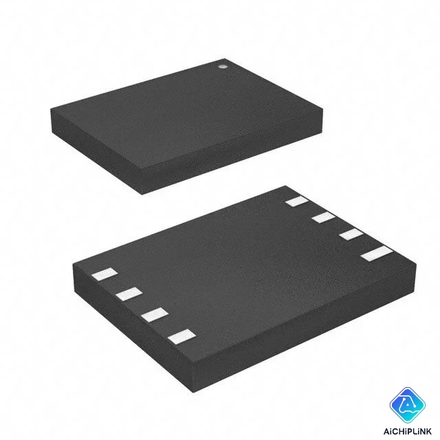
| Package | WSON-8 (8mm × 6mm) |
| Temperature | -40°C to +85°C (industrial) |
Part Number Decoder
MT29F2G01ABAGDWB breakdown:
- MT29F = Micron SPI NAND family
- 2G = 2 gigabit capacity
- 01 = Single die, x1 organization
- ABA = Technology/feature code
- GD = Speed grade
- WB = Package variant (WSON-8)
Key Features
Integrated ECC:
- Internal 1-bit ECC per 512 bytes
- Transparent error correction
- Status register reports correction
Simple SPI Interface:
- Standard 4-wire SPI (CS, CLK, MOSI, MISO)
- Dual and Quad SPI modes for higher throughput
- Compatible with most microcontrollers
Bad Block Management:
- Factory-marked bad blocks
- Spare area for bad block tables
- Typical <2% bad blocks at shipment
Low Power:
- Active read: 25 mA typical
- Standby: 25 μA typical
- Deep power-down: 10 μA
SPI NAND Architecture
NAND Flash Organization:
The MT29F2G01ABAGDWB uses hierarchical structure:
- Die → Blocks → Pages → Bytes
- 2048 blocks per device
- 64 pages per block (128KB)
- 2112 bytes per page (2048 data + 64 spare)
Page Structure:
Page (2112 bytes):
├─ Main area: 2048 bytes (user data)
└─ Spare area: 64 bytes (ECC, metadata, bad block marker)
Operations:
- Read: Page-level (2KB minimum)
- Program: Page-level (must be erased first)
- Erase: Block-level (128KB minimum)
Internal ECC:
- 1-bit correction per 512-byte chunk
- 4 ECC regions per 2KB page
- Automatic during read/program operations
- Status flags indicate correction performed
Complete Specifications
Memory Organization
| Parameter | Value |
|---|---|
| Total Capacity | 2,147,483,648 bits (2Gb) |
| User Data | 268,435,456 bytes (256MB) |
| Blocks | 2048 |
| Pages per Block | 64 |
| Bytes per Page | 2048 (main) + 64 (spare) |
Timing Specifications
| Operation | Typical | Maximum | Unit |
|---|---|---|---|
| Page Read | 25 | 60 | μs |
| Page Program | 300 | 700 | μs |
| Block Erase | 2 | 10 | ms |
| SPI Clock | - | 104 | MHz |
Endurance and Retention
| Parameter | Specification |
|---|---|
| Program/Erase Cycles | 100,000 (typical SLC) |
| Data Retention | 10 years @ 25°C |
| Read Disturb | 100,000 reads per block |
Electrical Specifications
| Parameter | Min | Typ | Max | Unit |
|---|---|---|---|---|
| Supply Voltage | 2.7 | 3.3 | 3.6 | V |
| Active Read Current | - | 25 | 30 | mA |
| Program Current | - | 30 | 40 | mA |
| Standby Current | - | 25 | 100 | μA |
| Deep Power-Down | - | 10 | 50 | μA |
Performance and SPI Interface
SPI Operating Modes
Standard SPI (x1):
- 4 wires: CS, CLK, SI (MOSI), SO (MISO)
- 1 bit per clock cycle
- Up to 104 MHz clock
- Throughput: ~13 MB/s read
Dual SPI (x2):
- Uses SI and SO as bidirectional data
- 2 bits per clock cycle
- Throughput: ~26 MB/s read
Quad SPI (x4):
- Requires additional pins (WP#, HOLD#)
- 4 bits per clock cycle
- Throughput: ~52 MB/s read
Command Set
Common Commands:
| Command | Opcode | Function |
|---|---|---|
| READ PAGE | 13h | Read page to cache |
| READ CACHE | 03h | Read from cache to SPI |
| PROGRAM LOAD | 02h | Load data to cache |
| PROGRAM EXECUTE | 10h | Program cache to page |
| BLOCK ERASE | D8h | Erase 128KB block |
| READ ID | 9Fh | Read device ID |
| GET FEATURE | 0Fh | Read status register |
Read Operation Sequence
1. Send PAGE READ command (13h) + 3-byte address
2. Wait for device ready (poll status register)
3. Send READ CACHE command (03h)
4. Clock out 2048 bytes of data
5. Check ECC status in feature register
Program Operation Sequence
1. Send WRITE ENABLE command (06h)
2. Send PROGRAM LOAD command (02h) + data
3. Send PROGRAM EXECUTE command (10h) + address
4. Wait for program complete (poll status)
5. Check status register for errors
Application Guidelines
Typical Applications
Embedded Systems:
- Firmware storage and boot code
- Data logging and event recording
- Configuration and calibration data
- File systems (JFFS2, YAFFS2, UBIFS)
IoT Devices:
- Sensor data buffering
- Over-the-air update storage
- Local data cache
- Low-power edge devices
Consumer Electronics:
- Set-top boxes
- Digital cameras
- Portable media players
- Smart home devices
Industrial:
- PLCs and industrial controllers
- Medical devices
- Automotive infotainment
- Point-of-sale terminals
System Integration
Microcontroller Interface:
MCU SPI ──┬── CS   ───► MT29F2G01ABAGDWB
          ├── SCLK ───►
          ├── MOSI ───► SI
          └── MISO ◄─── SO

Power Supply:
3.3V ──┬── VCC (MT29F2G01ABAGDWB)
       └── 0.1μF bypass capacitor
Boot Configuration:
- Not boot ROM (requires external controller)
- MCU boots from internal flash, then accesses SPI NAND
- Suitable for code storage via bootloader
Wear Leveling
Importance: NAND has limited P/E cycles (100K). Wear leveling distributes writes across blocks.
Implementation:
- Software wear leveling in file system driver
- Track erase counts per block
- Remap frequently written logical addresses to different physical blocks
Commercial Solutions:
- FTL (Flash Translation Layer) libraries
- File systems: JFFS2, YAFFS2, UBIFS, LittleFS
Bad Block Management
Factory Bad Blocks:
- Device ships with <2% bad blocks
- Marked in first byte of spare area (not 0xFF)
- Build bad block table at initialization
Runtime Bad Blocks:
- Monitor program/erase failures
- Mark new bad blocks in spare area
- Remap to spare blocks
Design Guidelines
PCB Layout
Trace Routing:
- Keep SPI traces short (<100mm)
- Match SI/SO trace lengths (±5mm)
- 50Ω controlled impedance for >50 MHz
- Ground plane under SPI signals
Decoupling:
- 0.1μF ceramic capacitor near VCC pin
- 10μF bulk capacitor on board
- Low ESR capacitors for high-speed operation
Clock Integrity:
- Minimize clock trace stubs
- Series termination resistor (22-33Ω) if ringing observed
- Keep clock away from noisy signals
Power Supply
Supply Voltage:
- 3.3V ±10% (2.7V - 3.6V)
- Clean, low-noise supply
- Avoid brownouts during erase/program
Power Sequencing:
- No specific requirement
- Can power up/down anytime
- Use RESET# for clean initialization
Software Considerations
File System Selection:
| File System | Best For | Wear Leveling |
|---|---|---|
| JFFS2 | Linux systems | Yes (built-in) |
| YAFFS2 | Embedded Linux | Yes (optimized for NAND) |
| UBIFS | Modern Linux | Yes (advanced) |
| LittleFS | MCU, RTOS | Yes (power-loss resilient) |
Driver Requirements:
- SPI peripheral driver
- NAND command protocol implementation
- Bad block handling
- ECC checking (read feature register)
Comparison and Alternatives
Micron SPI NAND Family
| Part Number | Capacity | Speed | Key Difference |
|---|---|---|---|
| MT29F1G01 | 1Gb (128MB) | 104 MHz | Half capacity |
| MT29F2G01ABAGDWB | 2Gb (256MB) | 104 MHz | Standard |
| MT29F4G01 | 4Gb (512MB) | 104 MHz | Double capacity |
vs Parallel NAND
| Feature | SPI NAND (MT29F2G01ABAGDWB) | Parallel NAND |
|---|---|---|
| Pin Count | 8 pins | 48+ pins |
| Interface | SPI (simple) | Parallel (complex) |
| PCB Area | Compact | Large footprint |
| Throughput | 13-52 MB/s | 40-100 MB/s |
| Best For | Embedded, space-constrained | High-performance storage |
vs eMMC
| Feature | SPI NAND (MT29F2G01ABAGDWB) | eMMC |
|---|---|---|
| Cost | Lower | Higher |
| Interface | SPI (4-8 pins) | MMC (10+ pins) |
| Controller | External (MCU) | Integrated |
| Capacity | 256MB | 4GB-256GB typical |
| Best For | Cost-sensitive, simple | High capacity, ease-of-use |
When to Choose SPI NAND (MT29F2G01ABAGDWB):
- ✅ Limited MCU pins (only 4 needed)
- ✅ Space-constrained designs
- ✅ Cost-sensitive applications
- ✅ Moderate storage needs (64MB-512MB)
Conclusion
The MT29F2G01ABAGDWB delivers reliable 2Gb (256MB) SPI NAND flash storage in compact package with simple 4-wire SPI interface, making it ideal for embedded systems requiring moderate capacity non-volatile memory without parallel NAND complexity or eMMC cost. With integrated ECC, industrial temperature range, and proven SLC endurance (100K cycles), it enables straightforward storage integration for IoT, industrial, and consumer applications.
Key Advantages:
✅ Simple Interface: 4-pin SPI (vs 16+ for parallel NAND)
✅ Adequate Capacity: 256MB for embedded firmware/data
✅ Integrated ECC: 1-bit correction per 512 bytes
✅ Low Cost: More economical than eMMC
✅ Compact: WSON-8 package (8mm × 6mm)
✅ Industrial Grade: -40°C to +85°C operation
Design with MT29F2G01ABAGDWB? Visit AiChipLink.com for technical resources and embedded storage design consultation.

Written by Jack Elliott from AIChipLink.
AIChipLink, one of the fastest-growing global independent electronic components distributors in the world, offers millions of products from thousands of manufacturers, and many of our in-stock parts is available to ship same day.
We mainly source and distribute integrated circuit (IC) products of brands such as Broadcom, Microchip, Texas Instruments, Infineon, NXP, Analog Devices, Qualcomm, Intel, etc., which are widely used in communication & network, telecom, industrial control, new energy and automotive electronics.
Empowered by AI, Linked to the Future. Get started on AIChipLink.com and submit your RFQ online today!
Frequently Asked Questions
What is MT29F2G01ABAGDWB?
MT29F2G01ABAGDWB is a 2-Gb (256 MB) SPI NAND flash memory from Micron Technology, designed for embedded and IoT systems that need higher-capacity non-volatile storage with a simple SPI interface and built-in ECC support.
How does MT29F2G01ABAGDWB connect to a microcontroller?
MT29F2G01ABAGDWB uses a standard 4-wire SPI interface (CS, SCLK, SI, SO) and requires a software driver to handle page-based read/write commands, status polling, and NAND management instead of simple byte addressing.
Can MT29F2G01ABAGDWB be used for direct boot?
No, MT29F2G01ABAGDWB does not support execute-in-place (XIP) boot, so a small bootloader in internal flash or external SPI NOR is required to load code from the SPI NAND into RAM.
What are the typical applications of MT29F2G01ABAGDWB?
MT29F2G01ABAGDWB is widely used for firmware storage, data logging, file systems, configuration data, and OTA update storage in embedded devices, industrial controllers, and consumer electronics.
Does MT29F2G01ABAGDWB require bad block management?
Yes, MT29F2G01ABAGDWB requires software-based bad block management and wear leveling, either through a NAND-aware file system or a custom flash translation layer to ensure long-term reliability.