Introduction
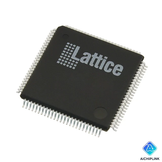
Picture this: your new PCB design needs to bridge two incompatible buses, manage a complex power-up sequence, and expand I/O — all while keeping BOM cost and footprint tiny. You could glue it together with discrete logic gates, but that means more parts, more risk, and a debugging nightmare. The LCMXO256C-3TN100C from Lattice Semiconductor was purpose-built to solve exactly this problem.
The global programmable logic device market is driven by the relentless demand for more system integration at lower cost and power — and low-density CPLDs and FPGAs like the MachXO family are right at the center of that trend. With 256 look-up tables (LUTs), 78 user I/Os, non-volatile flash configuration, and instant-on capability, the LCMXO256C-3TN100C punches well above its weight class.
In this complete guide, you'll get: a full technical breakdown, detailed pinout analysis, head-to-head comparisons with competing devices, a step-by-step programming walkthrough using Lattice Diamond, and expert sourcing advice. Let's get into it.
1.0 What Is the LCMXO256C-3TN100C? An Overview
The LCMXO256C-3TN100C is a member of Lattice Semiconductor's MachXO family — a line of non-volatile, infinitely reconfigurable programmable logic devices (PLDs) that combine the best attributes of traditional CPLDs and low-density FPGAs into a single device. It is designed for applications traditionally addressed by CPLDs: glue logic, bus bridging, bus interfacing, and power-up management.
Decoding the part number:
- LC — Lattice Corporation
- MXO — MachXO family (non-volatile, instant-on PLD)
- 256 — 256 look-up tables (LUTs) / logic density
- C — Commercial temperature grade (0°C to +85°C)
- -3 — Speed grade 3 (standard performance; faster grades available)
- TN100 — 100-pin TQFP package (Thin Quad Flat Package), 14×14 mm, 0.5 mm pitch
- C — Commercial temperature grade (confirmed)
"The MachXO family brings together the deterministic, instant-on behavior of CPLDs with the LUT-based flexibility of FPGAs — giving designers a single platform that eliminates the traditional trade-off between the two architectures."
Unlike SRAM-based FPGAs that require an external configuration PROM and a boot delay at power-on, the LCMXO256C-3TN100C stores its configuration in on-chip flash memory, meaning it is ready to operate immediately at power-up — a critical advantage in power sequencing and system management roles.
2.0 Full Technical Specifications & Architecture
2.1 Core Logic and Memory Parameters
Here is a complete summary of the key parameters from the LCMXO256C-3TN100C datasheet:
- Logic Density: 256 LUTs (Look-Up Tables)
- Macrocells: 128
- User I/O Pins: 78
- Distributed SRAM: 2.1 Kbits (embedded block RAM)
- Maximum Operating Frequency: 500 MHz (internal logic paths)
- Global Clock Setup Time (tSU): 1.8 ns
- Propagation Delay (tPD): 4.9 ns (pin-to-pin, combinatorial)
- PLLs: None in this density (available in higher MachXO densities)
- Configuration Memory: Non-volatile on-chip Flash (infinite reconfigurability)
- User Flash Memory: 2 Kbits (available for user data storage)
- Package: 100-pin TQFP (LFQFP), 14×14 mm body, 0.5 mm pitch
- Operating Temperature: 0°C to +85°C (commercial grade, "C" suffix)
- Supply Voltage (VCCIO): 1.71 V to 3.465 V (supports 1.8 V, 2.5 V, 3.3 V banks)
- Core Supply (VCC): 1.14 V to 1.33 V (nominal 1.2 V)
- MSL Rating: MSL 3 (168 hours floor life)
- RoHS Compliant: Yes (lead-free, matte tin finish)
- Lifecycle Status: Active / Production
The 4.9 ns pin-to-pin propagation delay is competitive with traditional CPLDs, making the LCMXO256C a genuine drop-in logic replacement for CPLD designs that need more density or flexibility. The 500 MHz internal frequency headroom ensures you won't hit timing walls even in aggressive registered logic pipelines.
2.2 Supported I/O Standards and Electrical Characteristics
The LCMXO256C-3TN100C supports a broad set of single-ended and differential I/O standards, making it highly versatile for multi-voltage system integration:
- Single-ended: LVCMOS 3.3 V / 2.5 V / 1.8 V, LVTTL, PCI (3.3 V), PCI-X
- Differential: LVDS (Low-Voltage Differential Signaling), Bus-LVDS, LVPECL
- Open-drain: Configurable per I/O pin for wired-OR topologies
- Programmable drive strength: 4 mA / 8 mA / 12 mA / 16 mA (per bank)
- Programmable slew rate control: Slow / Fast (per pin, to manage EMI)
- Hot-socketing: Supported (safe insertion/removal while system is powered)
- Weak pull-up / pull-down: Configurable per I/O pin
The multi-voltage I/O bank architecture means different banks of I/O pins can operate at different VCCIO levels simultaneously — a key feature when bridging between 3.3 V legacy interfaces and 1.8 V modern SoC or processor I/O.
2.3 Power Consumption and Non-Volatile Flash Configuration
One of the most compelling features of the MachXO family is its non-volatile flash-based configuration. Unlike SRAM FPGAs:
- No external configuration PROM required — the bitstream lives on-chip permanently
- Instant-on at power-up — logic is active in microseconds, not milliseconds
- Retains configuration through power cycles — no boot loading loop
- Infinitely reconfigurable — the on-chip flash endures 10,000+ erase/write cycles
Static power consumption in standby is extremely low — making this device suitable for battery-powered industrial sensors, embedded control modules, and any design where leakage current budget matters. The 1.2 V core voltage further reduces dynamic power versus 1.8 V or 3.3 V core architectures found in older CPLDs.
2.4 Typical Application Domains
The LCMXO256C-3TN100C excels in:
- Glue logic consolidation: Replace banks of 74-series gates with a single programmable device
- Bus bridging: Translate between SPI, I²C, parallel bus, and custom protocols
- Interface bridging: Convert voltage levels and timing between mixed-voltage subsystems
- Power-up sequencing: Implement power-rail sequencing and enable logic for multi-rail systems
- I/O expansion: Add GPIO capacity to an MCU or SoC with minimal overhead
- System management: Watchdog timers, reset controllers, LED drivers, and status monitors
- Communications equipment: Framing logic, protocol glue, and signal conditioning in line cards
3.0 Pinout and Package Details: 100-Pin TQFP
3.1 Key Functional Pin Groups
The 100-pin TQFP body measures 14 mm × 14 mm with a 0.5 mm pin pitch, placing it in the standard footprint range compatible with fine-pitch PCB processes (6 mil trace / space typically adequate). Key pin groups include:
- User I/O (78 pins): Distributed across multiple banks (Bank 0–2), each with independent VCCIO supply. Banks can be set to 1.8 V, 2.5 V, or 3.3 V independently.
- JTAG Interface (4 pins): TCK, TMS, TDI, TDO — used for programming, boundary scan, and debugging
- VCC pins (Core, 1.2 V nominal): Multiple pins — decouple each with 100 nF ceramics
- VCCIO pins (I/O bank supply): Separate per bank — allows mixed-voltage operation
- GND pins: Multiple ground pins distributed around the package perimeter
- DONE pin: Indicates configuration completion (useful for power sequencing logic)
- INITN pin: Active-low initialization input
Bank voltage configuration rule: All I/O pins within the same bank must share the same VCCIO level. Violating this will result in undefined behavior and potential latch-up. Refer to the Lattice MachXO Family Data Sheet for the exact bank pin assignments.
3.2 PCB Layout and Decoupling Guidelines
Good PCB layout is essential to realize the LCMXO256C's timing and noise performance:
- Decoupling (VCC core): Place one 100 nF X7R ceramic capacitor (0402 or 0201) per VCC pin, as close to the pin as possible. Add one 10 μF bulk cap per power rail cluster.
- Decoupling (VCCIO): Same approach per VCCIO bank — one 100 nF per VCCIO pin, one 10 μF bulk per bank.
- Ground plane: Use a solid unbroken ground plane directly beneath the device. Do not split the ground plane under the IC.
- JTAG routing: Keep TCK trace length under 5 cm; add a 33 Ω series termination resistor near the driver to reduce ringing.
- Differential pairs (LVDS): Route as tightly coupled differential pairs with 100 Ω differential impedance. Match trace lengths to within 5 mil.
- Power supply sequencing: If VCCIO is ramping before VCC, ensure VCC is at regulation before asserting any I/O-driven signals to avoid I/O bus contention during startup.
4.0 LCMXO256C-3TN100C vs. Competing CPLDs and Low-Density FPGAs
How does the LCMXO256C-3TN100C stack up against the most common alternatives? The table below provides a direct comparison:
| Feature | LCMXO256C-3TN100C | Lattice LCMXO2-256HC | Xilinx XC2C64A | Altera MAX II EPM240 |
|---|---|---|---|---|
| Architecture | MachXO (LUT + Flash) | MachXO2 (LUT + Flash) | CoolRunner-II (CPLD) | MAX II (CPLD/Flash) |
| Logic Density | 256 LUTs / 128 Macrocells | 256 LUTs / 192 Macrocells | 64 Macrocells | 240 Macrocells |
| User I/Os | 78 | 78 | 64 | 80 |
| Non-Volatile Config | Yes (on-chip Flash) | Yes (on-chip Flash) | Yes (EEPROM) | Yes (on-chip Flash) |
| Core Voltage | 1.2 V | 1.2 V | 1.8 V | 1.8 V |
| I/O Standards | LVDS, LVCMOS, LVPECL, PCI | LVDS, LVCMOS, LVPECL, PCI | LVDS, LVCMOS, SSTL | LVDS, LVCMOS, SSTL |
| Max Frequency | 500 MHz | 675 MHz | 263 MHz | 304 MHz |
| Package (100-pin) | TQFP-100 | TQFP-100 | TQG-100 | TQFP-100 |
| Toolchain | Lattice Diamond | Lattice Diamond | Xilinx ISE / Vivado | Intel Quartus Prime |
4.1 MachXO vs. MachXO2: When to Upgrade
The most direct upgrade path from the LCMXO256C-3TN100C is the LCMXO2-256HC (MachXO2 family). Here's when each device makes sense:
Choose LCMXO256C-3TN100C when:
- You need a proven, cost-optimized device for simple glue logic or bus bridging
- Your design is already qualified on the MachXO family
- BOM cost optimization is the top priority
- You need a pin-compatible device for an existing PCB layout
Upgrade to LCMXO2-256HC when:
- You need the hardened I²C/SPI slave port (eliminates external slave controller logic)
- Your application requires TransFR™ remote field upgrade capability
- You need PLL support (the MachXO2 has integrated PLLs not available in base MachXO)
- System clock requirements exceed the MachXO's 500 MHz internal capability
Both devices share the same 100-pin TQFP footprint and pin-compatible I/O bank structure, making migration straightforward at the PCB level.
5.0 Programming with Lattice Diamond and JTAG
5.1 Lattice Diamond Design Flow
The LCMXO256C-3TN100C is supported by Lattice Diamond, Lattice's free-to-download EDA toolchain. The complete design flow consists of:
- Design Entry: Write your logic in VHDL or Verilog HDL (or import a schematic)
- Synthesis: Diamond's integrated synthesis engine (or Synplify Pro for advanced optimization) compiles HDL to a gate-level netlist
- Map / Place & Route: Diamond maps the netlist onto MachXO LUTs, routes internal interconnects, and performs timing-driven placement
- Timing Analysis: Static timing analysis verifies setup, hold, and clock-to-output constraints against the device's -3 speed grade models
- Bitstream Generation: Diamond generates a
.jed(JEDEC) or.bitprogramming file - Device Programming: Use Diamond Programmer with a Lattice USB programming cable (HW-USBN-2B or compatible) to download the bitstream via JTAG
License note: Lattice Diamond is free for MachXO and MachXO2 family devices. No node-locked license is required, which is a significant advantage over Xilinx ISE (discontinued) and Intel Quartus for cost-conscious teams.
5.2 JTAG Programming and ispVM Configuration
The LCMXO256C-3TN100C supports JTAG-based in-system programming (ISP) via its four dedicated JTAG pins:
- TCK — Test Clock (up to 25 MHz recommended for reliable in-system programming)
- TMS — Test Mode Select
- TDI — Test Data Input
- TDO — Test Data Output (open-drain; add 10 kΩ pull-up to VCCIO)
JTAG programming sequence:
- Connect the Lattice programming cable to the JTAG header on your target board
- Open Diamond Programmer and select "Detect Cable"
- Select the LCMXO256C-3TN100C from the device scan list
- Load your
.jedbitstream file - Select "Program" — the on-chip flash is erased and reprogrammed in seconds
- Power cycle or assert INITN to reload the new configuration
For boundary scan and production test, the JTAG interface also exposes the full IEEE 1149.1 boundary scan chain, enabling structured board-level interconnect testing without bed-of-nails fixtures.
The video above walks through creating a new MachXO project in Lattice Diamond, synthesizing a Verilog design, running place-and-route, and programming the LCMXO256C-3TN100C via JTAG.
5.3 VHDL / Verilog Design Example: SPI-to-Parallel Bus Bridge
One of the most common real-world uses of the LCMXO256C-3TN100C is implementing a protocol bridge between an SPI master (MCU) and a parallel-bus peripheral. A conceptual Verilog implementation outline:
- Inputs:
SPI_CLK,SPI_CS_N,SPI_MOSI(from MCU) - Outputs:
PARALLEL_DATA[7:0],PARALLEL_WR_N,PARALLEL_ADDR[3:0](to peripheral) - Logic: 8-bit shift register clocked on SPI_CLK; on CS deassertion, latch to parallel output registers; decode address from upper nibble; assert PARALLEL_WR_N pulse
This logic occupies approximately 40–60 LUTs — well within the 256-LUT budget — leaving headroom for additional functions like a watchdog counter, reset controller, or status LED driver in the same device.
For more MachXO FPGA design examples and application notes, visit aichiplink.com FPGA resources.
6.0 How to Source Authentic LCMXO256C-3TN100C Units
Counterfeit programmable logic devices are a growing concern in the electronics supply chain. A remarked or cloned LCMXO256C may appear functional in basic testing but fail to meet timing specifications under temperature stress, or may not program reliably after multiple reprogram cycles. Here's how to protect your procurement:
- Verify the device marking: Genuine Lattice devices display "LCMXO256C-3TN100C" with Lattice Semiconductor's logo and a lot/date code. Use a 10× loupe to inspect for crisp, laser-etched characters — counterfeit parts often show ink-printed or re-marked markings.
- Check the JTAG ID: Authentic LCMXO256C devices return a specific JTAG IDCODE (0x01278043) when scanned. Read this via Diamond Programmer before committing to production. A mismatch is a definitive red flag.
- Request CoC and traceability: Authorized distributors provide a Certificate of Conformance (CoC) and lot traceability directly to Lattice's authorized distribution chain (Arrow, Avnet, Mouser, DigiKey).
- Test under temperature: If sourcing from secondary market, stress-test samples at 0°C and 85°C to verify timing margin holds across the rated commercial temperature range.
For verified inventory with full supply-chain traceability, competitive pricing, and RFQ support for both sample and volume orders, visit aichiplink.com — LCMXO256C-3TN100C listing.
8.0 Conclusion
The LCMXO256C-3TN100C occupies a uniquely valuable position in the programmable logic landscape: it delivers FPGA-style LUT-based flexibility with CPLD-style instant-on, non-volatile behavior — all in a compact, production-proven 100-pin TQFP package. Its 256 LUTs, 78 user I/Os, broad multi-voltage I/O standard support, and free Lattice Diamond toolchain make it one of the most cost-effective ways to consolidate glue logic, implement bus bridges, and manage power sequencing in any embedded design.
As systems grow more complex and multi-voltage, the need for flexible, low-latency interface logic will only increase. The MachXO family — with the LCMXO256C-3TN100C as its entry-level representative — is well positioned to serve that need for years to come, backed by Lattice's active production commitment and a wide ecosystem of application notes, reference designs, and third-party IP cores.
Ready to design with it? Explore verified inventory, request competitive pricing, and get expert sourcing support for the LCMXO256C-3TN100C at aichiplink.com — with fast fulfillment and complete documentation for every order.

Written by Jack Elliott from AIChipLink.
AIChipLink, one of the fastest-growing global independent electronic components distributors in the world, offers millions of products from thousands of manufacturers, and many of our in-stock parts is available to ship same day.
We mainly source and distribute integrated circuit (IC) products of brands such as Broadcom, Microchip, Texas Instruments, Infineon, NXP, Analog Devices, Qualcomm, Intel, etc., which are widely used in communication & network, telecom, industrial control, new energy and automotive electronics.
Empowered by AI, Linked to the Future. Get started on AIChipLink.com and submit your RFQ online today!
Frequently Asked Questions
What is the difference between the LCMXO256C-3TN100C and the LCMXO2-256HC-4TG100C?
Both are Lattice MachXO-family devices in 100-pin TQFP packages with 256 LUTs and 78 I/Os. The **LCMXO2-256HC** (MachXO2 generation) adds a **hardened I²C/SPI slave port**, a **PLL**, **TransFR™ remote field upgrade** capability, and a higher internal operating frequency. The LCMXO256C-3TN100C is the original MachXO generation — lower cost, simpler tool flow, and fully sufficient for pure glue logic and bus bridging applications that do not require PLLs or hardened serial slave interfaces.
Does the LCMXO256C-3TN100C need an external configuration PROM?
No. The MachXO family stores its configuration in **on-chip non-volatile flash memory**. The device powers up and begins executing logic within microseconds of VCC reaching the minimum operating voltage — no boot delay, no external PROM, no configuration controller required. This is one of its primary advantages over SRAM-based FPGAs like the Xilinx Spartan or Intel Cyclone families.
Can I use the LCMXO256C-3TN100C for power-up sequencing?
Yes — this is one of the classic MachXO applications. Because the device is **instantly active at power-up**, it can monitor VCC rail voltages (via GPIO thresholds), implement programmable delays, and sequence ENABLE signals to downstream power regulators in a defined order. This is far more flexible than discrete RC-based sequencers and easier to validate than microcontroller-based approaches that have their own boot delays.
What toolchain do I need to program the LCMXO256C-3TN100C?
Lattice Diamond is the primary EDA tool — it is free to download from Lattice's website and includes synthesis (synplify-based), place-and-route, timing analysis, and device programming. For the programming hardware, Lattice's **HW-USBN-2B** USB programming cable or any JTAG cable with Diamond Programmer driver support works. Legacy users can also use **ispVM System** (Lattice's older standalone programmer), though Diamond Programmer is preferred for all new designs.
Is the LCMXO256C-3TN100C still in production?
Yes. As of 2025, the **LCMXO256C-3TN100C** lifecycle status is listed as **Active / Production** by Lattice Semiconductor. It is available through authorized distributors including DigiKey, Mouser, and Arrow with standard lead times. For bulk procurement or time-sensitive sourcing, Aichiplink provides verified stock with expedited fulfillment options.