Introduction
If you've ever tried to interface a microcontroller with an industrial 4–20 mA current loop — only to spend hours wrestling with external op-amps, current mirrors, and noise-susceptible analog circuits — you know the pain. The AD5420ACPZ from Analog Devices, Inc. eliminates that complexity in a single, highly integrated IC.
According to IEC 60381-1, the 4–20 mA current loop is the global standard for transmitting process variables in industrial automation — used in more than 70% of all field instrumentation worldwide. Getting precise, stable current output from a digital controller has never been more critical, and at 16-bit resolution, the AD5420ACPZ sets the bar in its class.
In this complete guide you'll find: a full technical breakdown, SPI programming walkthroughs, real-world application examples, head-to-head comparisons with competing DACs, and expert sourcing tips. Whether you're a hardware engineer qualifying this part or a procurement specialist tracking availability, you're in the right place.
1.0 What Is the AD5420ACPZ? An Overview
The AD5420ACPZ is a single-channel, 16-bit, fully integrated current source DAC (Digital-to-Analog Converter) manufactured by Analog Devices. It is specifically engineered for industrial process control — the demanding environment where signal accuracy, reliability, and fault tolerance are non-negotiable.
Decoding the part number reveals key attributes:
- AD5420 — 16-bit current source DAC (AD5410 = 12-bit sibling)
- A — Standard silicon process
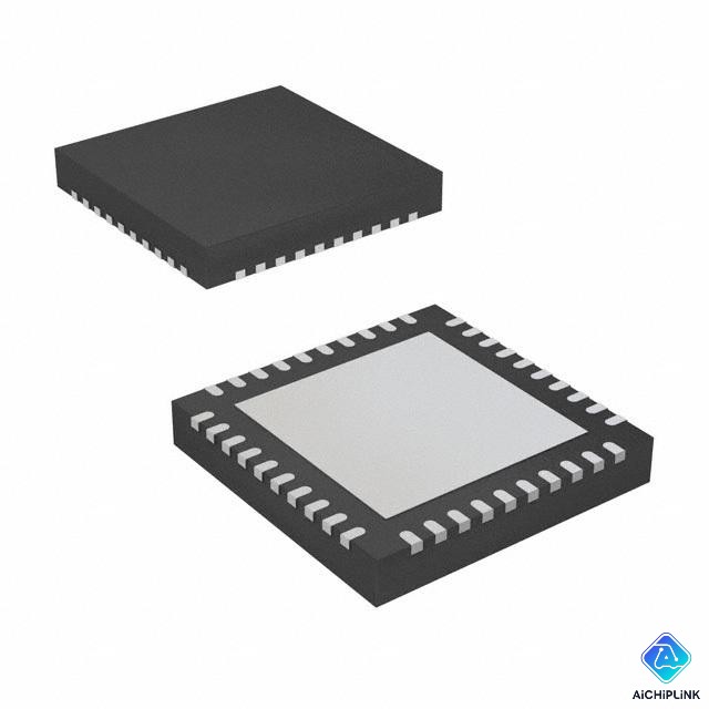
- CPZ — 40-lead LFCSP (Lead Frame Chip Scale Package), 6 mm × 6 mm, with exposed pad, RoHS compliant
The device outputs a precisely controlled current in three programmable ranges: 4 mA to 20 mA, 0 mA to 20 mA, or an extended 0 mA to 24 mA overrange. It accepts digital input over a SPI/QSPI/MICROWIRE/DSP-compatible serial interface, making it trivial to connect to virtually any modern microcontroller or DSP.
"The AD5420 delivers the integration and precision that industrial automation engineers have long demanded in a 4–20 mA transmitter IC, without external amplifiers or complex calibration routines."
2.0 Full Technical Specifications & Datasheet Highlights
2.1 Core Electrical Parameters
Here is a consolidated view of the critical electrical characteristics from the AD5420ACPZ datasheet:
- Resolution: 16 bits (65,536 codes)
- Output Current Ranges: 4–20 mA | 0–20 mA | 0–24 mA (overrange)
- Analog Supply (AVDD): 10.8 V to 60 V
- Digital Supply (DVDD): 2.7 V to 5.5 V
- Output Loop Compliance: 0 V to AVDD − 2.5 V
- INL / DNL: ±0.15 LSB typical / ±1 LSB maximum
- Output Noise: 35 nA rms (1 Hz to 1 kHz)
- Internal Reference: 5 V ± 2 mV (can also accept 4–5 V external reference)
- Power-On Reset: Yes — outputs default to low end of range
- CLEAR Pin: Asynchronous, active-low, sets output to low end
- Operating Temperature: −40°C to +85°C
- Package: 40-lead LFCSP (6 mm × 6 mm with exposed pad)
- RoHS Compliant: Yes (Z suffix)
The ±0.15 LSB typical INL makes this one of the most linear current DACs in the 4–20 mA class. In a 16 mA full-scale span (4–20 mA), each LSB equals approximately 244 nA — translating to better than 0.04 μA accuracy at typical INL. That precision matters when your sensor calibration window is tight.
2.2 Pin Configuration and LFCSP Package Details
The 40-lead LFCSP package (6 mm × 6 mm, 0.5 mm pitch) is compact and thermally efficient thanks to its exposed pad that bonds directly to a ground plane. Key functional pins include:
- IOUT (Pin 11): Current output pin — connect to the 4–20 mA loop
- IOUT_EXT (Pin 12): Optional external transistor connection for power reduction
- REFOUT (Pin 6): 5 V internal reference output
- REFIN (Pin 7): External reference input (4–5 V range)
- SDIN, SCLK, SYNC, SDO (Pins 34–37): SPI serial interface
- CLEAR (Pin 38): Active-low async clear
- FAULT (Pin 39): Open-drain fault indicator (open-circuit / overtemp)
- AVDD (Pins 1–3): Analog supply, 10.8–60 V
- DVDD (Pin 33): Digital supply, 2.7–5.5 V
Layout tip: Place a 10 μF bulk capacitor and a 100 nF decoupling capacitor on AVDD as close to the IC as physically possible. Keep the AGND pour separate from DGND, connecting only at a single star point near the exposed pad.
2.3 HART Connectivity and 3-Wire SPI Mode
One of the most valuable features of the AD5420ACPZ is its 3-wire SPI mode, which is specifically designed to minimize the number of signal lines crossing an isolation barrier in HART-enabled transmitters. HART (Highway Addressable Remote Transducer) superimposes a 1200 Hz / 2200 Hz FSK signal on top of the 4–20 mA loop.
In 3-wire mode, the SDO line is eliminated, reducing the isolation channel count. When combined with Analog Devices' ADuM1400 quad digital isolator, you can build a fully isolated HART-compatible transmitter without an external DAC buffer — a significant board-space and cost saving.
3.0 Industrial Applications: 4–20 mA Process Control
3.1 PLC and DCS Interface Design
In a typical process control system, the AD5420ACPZ sits inside a field transmitter or analog output module connected to a PLC (Programmable Logic Controller) or DCS (Distributed Control System). The PLC sends a digital set-point via SPI; the AD5420ACPZ outputs the corresponding 4–20 mA current to a control valve, actuator, or signal conditioner.
A complete transmitter design typically includes:
- Power conditioning: A DC-DC converter steps down the 24 V loop supply to AVDD
- Digital isolation: ADuM1400 or similar for SPI lines across HART isolation barrier
- AD5420ACPZ: 16-bit DAC producing calibrated 4–20 mA output
- Loop monitoring: Sense resistor and ADC for current readback verification
- Microcontroller: MCU running the HART physical layer stack and PLC interface
3.2 Open-Circuit Protection and Fault Handling
The AD5420ACPZ includes open-circuit protection on the IOUT pin — if the current loop is disconnected, the device clamps to a safe state and asserts the FAULT pin (open-drain, active-low). This is critical in safety-instrumented systems (SIS) where a broken loop must be detectable without damage to the transmitter.
The FAULT pin also activates for over-temperature conditions (junction temperature > 150°C), giving the host MCU an early warning to reduce output or initiate a safe shutdown. Combine this with a watchdog timer on the MCU for a robust, IEC 61508-aware design.
3.3 Thermal Management and External Transistor Option
At high AVDD voltages and maximum output currents, power dissipation inside the AD5420ACPZ can be substantial. For example, at AVDD = 60 V and IOUT = 24 mA with a 100 Ω load, the internal power dissipation is approximately:
P = (AVDD − VLOAD) × IOUT = (60 − 2.4) × 0.024 ≈ 1.38 W
The 40-lead LFCSP's exposed pad allows θJA ≈ 24°C/W with good PCB ground copper, giving a junction temperature rise of ~33°C above ambient — manageable, but worth monitoring.
For higher voltage applications, Analog Devices recommends the external transistor option: connect a power NPN transistor to the IOUT_EXT pin. The AD5420ACPZ then drives the transistor's base, offloading the bulk of power dissipation to the external device and enabling supply voltages up to 60 V without stressing the IC's internal pass element.
4.0 AD5420ACPZ vs. Competing Current Source DACs
How does the AD5420ACPZ compare to its closest competitors? The table below benchmarks it against its 12-bit sibling, Texas Instruments' DAC8760, and the TI XTR117:
| Feature | AD5420ACPZ | AD5410ACPZ | TI DAC8760 | TI XTR117 |
|---|---|---|---|---|
| Resolution | 16-bit | 12-bit | 16-bit | N/A (V-to-I) |
| Output Range | 0–20 mA / 4–20 mA / 0–24 mA | 0–20 mA / 4–20 mA / 0–24 mA | 0–20 mA / 4–20 mA | 4–20 mA (loop-powered) |
| Supply Voltage | 10.8 V – 60 V | 10.8 V – 60 V | 10.8 V – 60 V | 7.5 V – 36 V |
| HART Support | Yes (3-wire SPI mode) | Yes (3-wire SPI mode) | Yes | No |
| Package | 40-lead LFCSP (6×6 mm) | 40-lead LFCSP / 24-lead TSSOP | 48-lead HTSSOP | SOT-23-5 |
| Temp Range | −40°C to +85°C | −40°C to +85°C | −40°C to +105°C | −40°C to +125°C |
The key advantage of the AD5420ACPZ over the AD5410 is straightforward: four additional bits of resolution (16-bit vs. 12-bit), lowering the LSB step size from ~3.9 μA to ~244 nA in the 4–20 mA range — a 16× improvement in granularity. Against the TI DAC8760, the AD5420ACPZ edges ahead with its smaller 40-lead LFCSP footprint (6×6 mm vs. 48-lead HTSSOP), while matching it on resolution and HART support.
The TI XTR117 occupies a different niche: it's a loop-powered V-to-I converter that requires an external voltage DAC and offers no native digital interface — making it more suitable for legacy 4–20 mA retrofits than new digital designs.
5.0 SPI Programming, Configuration & Code Examples
5.1 Register Map and Control Word Structure
The AD5420ACPZ is configured by writing 24-bit words over SPI. Each word consists of an 8-bit register address and a 16-bit data payload. The two most important registers are:
- Control Register (0x55): Sets output range (4–20 mA / 0–20 mA / 0–24 mA), enables REXT (external reference), powers on the DAC, and clears fault flags
- Data Register (0x01): Accepts 16-bit output code. Code
0x0000= minimum current;0xFFFF= maximum current
For the 4–20 mA range: Output (mA) = 4 + (Code / 65535) × 16. So to output exactly 12 mA (midscale), write Code = 32767 (0x7FFF) to the Data Register.
5.2 Microcontroller Integration (Arduino / STM32 Example)
Below is a conceptual Arduino-style initialization sequence for the AD5420ACPZ:
- Step 1: Configure SPI: Mode 1 (CPOL=0, CPHA=1), MSB first, max 30 MHz clock
- Step 2: Assert SYNC low (CS active)
- Step 3: Send
0x55followed by0x0010to Control Register (select 4–20 mA, power on, internal ref) - Step 4: Deassert SYNC high — latch control word
- Step 5: Assert SYNC low again
- Step 6: Send
0x01followed by 16-bit output code (e.g.,0x7FFFfor 12 mA) - Step 7: Deassert SYNC — current output immediately updates
For STM32 users, HAL_SPI_Transmit() with DMA in circular mode allows continuous smooth current updates at rates up to several kHz — more than adequate for any 4–20 mA control loop.
For more Analog Devices DAC integration code samples, visit aichiplink.com DAC resources for curated application notes and design references.
6.0 How to Source Authentic AD5420ACPZ Units
6.1 Identifying Genuine Analog Devices Parts
Counterfeit ICs — especially popular industrial components like the AD5420ACPZ — are a real and costly problem. A cloned or re-marked part may boot up and respond to SPI, yet exhibit dramatically worse INL, temperature drift, or premature failure under industrial cycling stress. Here's how to protect yourself:
- Verify marking: The top of the IC should read "AD5420ACPZ" with Analog Devices' logo and a date/lot code. Examine under magnification for crisp, laser-etched characters — not inkjet or hand-stamped.
- Check the exposed pad: Genuine LFCSP parts have a clean, centered metal pad on the bottom. Re-balled counterfeit parts often show uneven solder residue.
- Electrical test: Power up with AVDD = 24 V, write a midscale code, measure IOUT with a calibrated current meter. Genuine parts hit 12.000 mA ±0.03 mA. Counterfeits often show >0.5% deviation.
- Demand documentation: Reputable distributors provide a Certificate of Conformance (CoC), date-code traceability to Analog Devices' authorized distribution, and anti-counterfeit test results.
6.2 Evaluation Board: EVAL-AD5420EBZ
Before committing to a production design, Analog Devices recommends prototyping with the EVAL-AD5420EBZ evaluation board. It includes a fully populated AD5420ACPZ circuit, USB-to-SPI bridge, loop power connector, and PC-based GUI for register-level testing — ideal for quickly validating your PCB layout and firmware before tape-out.
For production procurement of the AD5420ACPZ — whether you need single-piece samples or volume orders — visit aichiplink.com — AD5420ACPZ listing. Our team provides verified inventory with full supply-chain traceability, competitive pricing, and RFQ support for volume requirements.
Conclusion
The AD5420ACPZ stands out as the definitive solution for engineers who need precision 4–20 mA current output from a digital control system. Its 16-bit resolution, wide 10.8–60 V supply range, full ESD and open-circuit protection, built-in HART-compatible SPI mode, and compact 6×6 mm LFCSP package make it the go-to choice in industrial process control, flow metering, temperature transmitters, and smart valve positioners.
As industrial IoT and Industry 4.0 continue to push for smarter, more connected field instruments, components like the AD5420ACPZ — which seamlessly bridge the digital and analog worlds — will only grow in strategic importance. Its long production lifecycle, deep ecosystem of evaluation tools, and Analog Devices' global support network make it a safe bet for designs that need to be supported for a decade or more.
Ready to get started? Explore verified inventory, competitive pricing, and expert procurement support for the AD5420ACPZ at aichiplink.com today — with fast turnaround and full documentation available for every order.

Written by Jack Elliott from AIChipLink.
AIChipLink, one of the fastest-growing global independent electronic components distributors in the world, offers millions of products from thousands of manufacturers, and many of our in-stock parts is available to ship same day.
We mainly source and distribute integrated circuit (IC) products of brands such as Broadcom, Microchip, Texas Instruments, Infineon, NXP, Analog Devices, Qualcomm, Intel, etc., which are widely used in communication & network, telecom, industrial control, new energy and automotive electronics.
Empowered by AI, Linked to the Future. Get started on AIChipLink.com and submit your RFQ online today!
Frequently Asked Questions
What is the difference between the AD5420ACPZ and the AD5410ACPZ?
The only difference is **resolution**. The AD5420ACPZ offers **16-bit (65,536 codes)** while the AD5410ACPZ offers **12-bit (4,096 codes)**. All other specs — supply voltage, output range, package, SPI interface, HART support, and temperature rating — are identical. Choose the AD5420ACPZ when your process requires better than 0.05% accuracy; the AD5410ACPZ is sufficient for less demanding applications.
Can the AD5420ACPZ operate with a 3.3 V microcontroller?
Yes. The digital supply (DVDD) accepts 2.7 V to 5.5 V, so 3.3 V MCUs (STM32, nRF52, ESP32) connect directly to the SPI interface without level translators. The SPI logic thresholds scale with DVDD, so ensure your MCU SPI output voltage (≥ 0.7 × DVDD for logic high) meets the spec.
How do I implement HART communication with the AD5420ACPZ?
The AD5420ACPZ handles the **4–20 mA analog current output** side of the loop; HART FSK modulation is added on top of the loop by a separate **HART modem IC** (such as the AD5700 from Analog Devices). The AD5420's 3-wire SPI mode minimizes isolation channels, making it easy to bridge the digital side across an isolation barrier (e.g., using ADuM1400) while the HART modem connects directly to the loop on the other side.
What causes the AD5420ACPZ FAULT pin to assert?
Two conditions trigger the open-drain FAULT pin: (1) **Open-circuit output** — the current loop is broken, so IOUT cannot source the requested current; (2) **Over-temperature** — the die junction temperature exceeds approximately 150°C. Both conditions are reported simultaneously in the Status Register, which you can read back via SPI to distinguish between the two fault types.
Is the AD5420ACPZ pin-compatible with other current DACs?
The AD5420ACPZ (40-lead LFCSP) is **pin-compatible with the AD5410ACPZ**. It is **not** pin-compatible with the AD5420AREZ (24-lead TSSOP package) — a different package with a different footprint and pin assignment, despite being functionally similar. Always verify the exact package variant when designing for drop-in compatibility.