Introduction
Current measurement is one of the most fundamental tasks in power electronics and embedded systems design — yet it is also one of the most frequently done poorly. Hall-effect sensors are bulky and expensive. Low-side shunt resistors disturb the ground reference and prevent direct load-ground connection. Transformer-based methods fail at DC. For the vast majority of practical applications — battery chargers, motor controllers, power supplies, USB power delivery monitors, and load protection circuits — a high-side current shunt monitor is the technically superior and cost-effective solution.
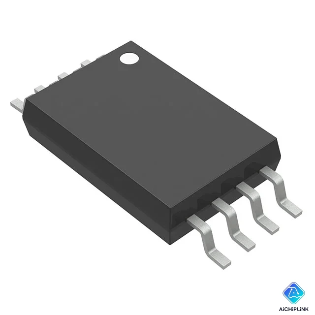
The INA139 from Texas Instruments is one of the most enduring and widely used devices in this category. First introduced as part of TI's Burr-Brown precision analog portfolio, the INA139 has been in continuous production for over two decades — a testament to its elegance: a single 5-pin SOT-23 IC that converts a high-side shunt resistor voltage drop into a proportional current output, allowing any engineer to build a precision current measurement circuit with just two external resistors, consuming only 60 µA of quiescent current, operating across a common-mode range of 2.7 V to 40 V, and fitting into the smallest available SMT footprint.
According to TI's Current Sensing product family overview, high-side current sensing is preferred in automotive, industrial, and portable electronics whenever ground-reference integrity, EMI immunity, and load circuit transparency are required — all conditions where the INA139's architecture excels.
This guide provides the complete specification analysis, gain design formulas, practical circuit examples, head-to-head comparisons, PCB layout rules, and sourcing guidance for the INA139.
1.0 What Is the INA139? An Overview
The INA139 is a high-side, unipolar current shunt monitor manufactured by Texas Instruments. It is a member of the INA1x9 family (INA139 and INA169), designed to measure DC load current flowing through a series shunt resistor placed on the high side (positive supply rail) of a load circuit, and to produce an output voltage proportional to that current — using only two external resistors to set the measurement gain.
Decoding the ordering codes:
- INA139NA — 5-pin SOT-23 (PW package), standard commercial grade (−40°C to +85°C), bulk tray packaging
- INA139NAQDBVRQ1 — 5-pin SOT-23 (DBV), AEC-Q100 automotive-qualified (−40°C to +125°C), tape-and-reel
- INA139-Q1 — Generic designator for the automotive-qualified variant family
The INA169 is the higher-voltage sibling: electrically identical to the INA139 in architecture, transconductance, and package, but rated for common-mode voltages up to 60 V (versus 40 V for INA139) — enabling use in 48 V automotive, 24–36 V industrial, and solar panel monitoring applications.
"The INA139 and INA169 are high-side, unipolar, current shunt monitors. The device converts a differential input voltage to a current output. This current is converted back to a voltage with an external load resistor that sets any gain from 1 to over 100." — Texas Instruments INA1x9 Datasheet, Rev. F
The transconductance-output architecture — producing a current rather than a voltage at the output pin — is the INA139's key architectural distinction from fixed-gain current sense amplifiers (like the INA219 or INA226). It gives designers complete freedom to set any gain from 1 V/V to over 100 V/V simply by choosing a single external resistor RL value, without needing to match a resistor ratio to achieve a specific gain.
2.0 Full Technical Specifications & Transconductance Architecture
2.1 Core Electrical Parameters
The following parameters are drawn from the TI INA1x9 datasheet (Rev. F), at V+ = 5 V, VIN+ = 12 V, TA = 25°C unless noted:
- Common-Mode Input Voltage Range (VCM): 2.7 V to 40 V (INA139); independent of V+ supply
- Power-Supply Voltage (V+): 2.7 V to 40 V (same range; V+ and VCM are independently set)
- Transconductance (gm): 1000 µA/V (fixed, internal)
- Maximum Differential Input Voltage (VIN+ − VIN−) for accurate measurement: 500 mV (produces 500 µA output current)
- Maximum Differential Input Voltage without damage: 2.0 V
- Input Offset Voltage (VOS): ±1 mV typical
- Input Bias Current (IB): ±5 µA typical (note: must be accounted for with high-value RS)
- Quiescent Current (IQ): 60 µA typical (entire device, V+ to GND)
- Output Current (IO) Range: 0 to 500 µA (corresponding to VIN differential of 0 to 500 mV)
- Output Load Resistor (RL) Range: 0 to 100 kΩ (higher RL = higher gain; output impedance is very high)
- Gain Range: 1 V/V to > 100 V/V (set by RL / RS ratio × gm)
- Bandwidth (−3 dB): ~200 kHz at RL = 10 kΩ (gain-bandwidth product follows RL dependency)
- Operating Temperature Range: −40°C to +85°C (commercial); −40°C to +125°C (automotive Q1)
- Package: 5-pin SOT-23 (DBV/PW variants)
- RoHS Compliant: Yes
- ESD Rating: ±2 kV (HBM)
The 60 µA quiescent current is a defining characteristic — it is low enough that the IQ error contribution to the current measurement (through the shunt resistor) is negligible in most applications, and it permits powering the INA139 from either side of the shunt resistor without introducing meaningful measurement offset. In a 1 A current measurement with a 100 mΩ shunt, the 60 µA IQ flowing through the shunt contributes only 6 µV of offset error — less than 0.006% of full scale.
2.2 Transconductance Architecture: gm = 1000 µA/V
The INA139's internal circuit elegantly solves the high-side measurement problem with a small number of components:
How it works:
The internal operational amplifier monitors the differential voltage across an internal input resistor RG1, and forces this same voltage to appear across the shunt resistor RS connected at the VIN+ and VIN− pins. This forces a current through Q1, an NPN transistor whose collector current becomes the output current IO. The relationship is:
IO = gm × (VIN+ − VIN−) = 1000 µA/V × VS
where VS = IS × RS is the shunt voltage (the voltage drop across the shunt resistor due to load current IS).
The external resistor RL, connected between the OUT pin and GND, converts this output current to an output voltage:
VOUT = IO × RL = gm × VS × RL = gm × IS × RS × RL
Complete transfer function:
VOUT = IS × RS × RL × gm = IS × RS × RL × 0.001 A/V
Or equivalently, the voltage gain of the measurement circuit is:
AV = VOUT / VS = RL × gm = RL (kΩ) × 1 V/V per kΩ
This means: each 1 kΩ of RL provides 1 V/V of gain — a beautifully simple, linear relationship that makes gain selection trivially easy:
| RL Value | Voltage Gain (AV) | Full-Scale VOUT (at VS = 100 mV) |
|---|---|---|
| 1 kΩ | 1 V/V | 0.1 V |
| 5 kΩ | 5 V/V | 0.5 V |
| 10 kΩ | 10 V/V | 1.0 V |
| 25 kΩ | 25 V/V | 2.5 V |
| 50 kΩ | 50 V/V | 5.0 V |
| 100 kΩ | 100 V/V | 10.0 V |
The very high output impedance of the INA139's OUT pin means the RL resistor defines the gain — no feedback resistors, no matched resistor pairs, no ratio errors. Any output loading (ADC input impedance, downstream amplifier input) appears in parallel with RL and must be accounted for in gain calculations.
2.3 Common-Mode Range, Quiescent Current, and Supply Flexibility
One of the INA139's most useful engineering characteristics is the independence of its power supply (V+) from the measured common-mode voltage (VCM). In many current sense applications, the load voltage (and therefore the shunt resistor common-mode voltage) is different from the available logic-supply voltage:
- A 12 V automotive battery load (VCM = 12 V) with a 3.3 V microcontroller supply (V+ = 3.3 V)
- A 24 V industrial bus (VCM = 24 V) with a 5 V analog supply (V+ = 5 V)
- A 36 V brushless motor (VCM = 36 V) with a 3.3 V DSP supply (V+ = 3.3 V)
In all these cases, the INA139's V+ pin connects to the lower logic supply voltage, while the VIN+ and VIN− pins connect directly to the high-side shunt resistor at the higher bus voltage. The internal circuitry correctly measures the shunt voltage across the full 2.7 V to 40 V common-mode range, regardless of V+ level — as long as V+ ≥ 2.7 V.
This independence also means the INA139 can measure above its own V+ supply voltage. For example, with V+ = 5 V, the INA139 can measure current on a 12 V, 24 V, or 36 V bus — the common-mode input range is set by the process limits of the input stage, not by the V+ rail.
2.4 High-Side vs. Low-Side Current Measurement
Understanding why high-side measurement is often preferable to low-side is essential context for the INA139's design philosophy:
Low-side measurement (shunt between load and GND):
- Simple circuit: shunt voltage directly measurable by any single-ended ADC referenced to GND
- Fatal flaw: the load's ground connection is not at system ground — it floats by VS = IS × RS above GND. In a motor controller, this shifts the entire motor's ground reference, potentially causing shoot-through in half-bridge drivers, ground loops in encoder feedback circuits, and shield grounding faults in cable-connected loads.
- Additional flaw: provides no protection against wiring faults — a short from load terminal to chassis ground is undetectable by a low-side monitor.
High-side measurement (shunt between supply and load — INA139 approach):
- The load's ground connection remains at true system ground — no ground reference disturbance
- Detects both overcurrent and short-to-ground conditions — any fault current flows through the shunt
- Required for reverse-polarity protection circuits (the shunt monitors current from both the forward load and any reverse-connected battery)
- Complexity cost: the shunt voltage is at a high common-mode voltage, requiring a differential measurement technique — exactly what the INA139 provides
For these reasons, high-side current sensing with the INA139 is the standard approach in battery management systems, automotive load circuits, and safety-critical power monitoring applications where ground reference integrity is non-negotiable.
3.0 Circuit Design and Application Examples
3.1 Basic Current Sense Circuit: RS and RL Selection
Designing a complete INA139 current sensing circuit requires selecting two external resistors: the shunt resistor RS (in series with the load, sets measurement resolution vs. power loss) and the load/gain resistor RL (from OUT pin to GND, sets output voltage scale).
Step 1: Select RS based on maximum current and acceptable voltage drop
The INA139 measures accurately up to a maximum shunt voltage of 500 mV (full-scale IO = 500 µA). TI recommends designing for a full-scale VS of 50 mV to 100 mV for best accuracy — the offset voltage errors are a smaller fraction of the signal, while the power loss in the shunt remains manageable.
RS = VS_max / IS_max
For a 5 A maximum current with VS_max = 100 mV:
RS = 0.1 V / 5 A = 20 mΩ
Power dissipated in RS at full scale: P = IS² × RS = 25 × 0.02 = 0.5 W — requires a 1 W or higher rated shunt resistor (e.g., Vishay WSL2512 series, 20 mΩ, 1 W).
Step 2: Select RL for the desired output voltage range
The full-scale output voltage should match the ADC's input range (typically 0–3.3 V, 0–2.5 V, or 0–5 V):
RL = VOUT_full_scale / IO_full_scale = VOUT_full_scale / (gm × VS_max)
For VOUT_max = 3.3 V and VS_max = 100 mV:
RL = 3.3 V / (0.001 × 0.1) = 3.3 V / 100 µA = 33 kΩ
Verify the complete transfer function:
VOUT = IS × RS × RL × gm = IS × 0.02 × 33000 × 0.001 = IS × 0.66 V/A
At IS = 5 A: VOUT = 3.3 V ✓ (matches ADC full-scale)
Practical RS selection table for common current ranges:
| Max Current | VS_max | RS Value | RS Power Rating | RL for 3.3V VOUT |
|---|---|---|---|---|
| 500 mA | 50 mV | 100 mΩ | 0.05 W (1/4 W) | 66 kΩ |
| 1 A | 100 mV | 100 mΩ | 0.1 W (1/4 W) | 33 kΩ |
| 5 A | 100 mV | 20 mΩ | 0.5 W (1 W) | 33 kΩ |
| 10 A | 100 mV | 10 mΩ | 1.0 W (2 W) | 33 kΩ |
| 20 A | 50 mV | 2.5 mΩ | 0.5 W (1 W) | 66 kΩ |
Use 1% tolerance resistors for both RS and RL to keep gain error below ±2%. For RS specifically, use 4-terminal (Kelvin) shunt resistors in high-current (> 5 A) applications to eliminate PCB trace resistance from the measurement.
3.2 ADC Interface, Output Buffering, and Low-Pass Filtering
ADC loading effect: The INA139's OUT pin output impedance is very high — the measured voltage equals IO × RL only if the ADC input impedance is much larger than RL. Most SAR ADCs have an input impedance of 10 kΩ to 1 MΩ (switching), depending on the sampling capacitor and sample rate. If the ADC input impedance (RADC) is comparable to RL, the actual gain is reduced:
VOUT_actual = IO × (RL ∥ RADC)
For a 10-bit ADC with 50 kΩ input impedance and RL = 33 kΩ, the effective resistance is 33k ∥ 50k = 19.7 kΩ — a 40% gain error. Solutions:
- Include RADC in the effective RL calculation: If the ADC input impedance is stable and well-characterized, design RL such that RL ∥ RADC achieves the target gain.
- Buffer with a unity-gain op-amp: Insert an op-amp voltage follower (e.g., TLV2401, OPA340) between the RL node and the ADC. The op-amp's high input impedance eliminates ADC loading; its low output impedance drives the ADC sampling capacitor cleanly.
Low-pass output filter: The INA139 output bandwidth at a given RL is approximately:
f_−3dB ≈ gm / (2π × RL × C_internal)
A simple external low-pass filter is formed by placing a capacitor CF in parallel with RL:
f_corner = 1 / (2π × RL × CF)
For RL = 33 kΩ and a desired 1 kHz noise bandwidth (suitable for battery current monitoring): CF = 1 / (2π × 33k × 1000) = 4.8 nF (use 4.7 nF standard value).
This RC filter attenuates switching noise from PWM motor controllers, inverters, and switch-mode power supplies that would otherwise alias into the current measurement.
3.3 Bipolar (Bidirectional) Current Measurement
The INA139 is inherently unipolar — it measures current flowing in one direction only (positive VS at VIN+, meaning current flowing from supply to load through the shunt). When the current reverses (VIN+ < VIN−), the output current IO goes to zero, not negative.
For applications requiring bidirectional current measurement (motor regenerative braking, battery charge/discharge monitoring, bidirectional DC-DC converters), TI's recommended approach uses two INA139 devices plus a polarity detector:
- Connect both INA139s with their inputs across the same shunt resistor, but with opposite polarity — one measuring positive current, one measuring negative current
- Use a comparator (e.g., TLV3201) to detect the sign of the load current
- Each INA139 produces a positive output voltage proportional to current in its direction; the comparator selects which output is valid
- A diode on each INA139 output prevents back-current from flowing into the inactive device's output
This dual-INA139 bidirectional circuit provides the full accuracy of the INA139 in both current directions, with output magnitude always positive — suitable for microcontroller ADC inputs without negative-rail requirements.
Alternatively, an output voltage offset applied to one INA139 channel can shift the idle output above zero, allowing the ADC to resolve both positive and negative current as a mid-scale offset signal — the simplest single-device approach for moderate-accuracy bidirectional sensing.
3.4 Battery Management, Motor Control, and Overcurrent Detection
This video covers INA139 transconductance architecture, RS and RL design methodology, common-mode independence, ADC interface techniques, and practical application circuits for battery monitoring, motor control, and overcurrent protection.
Battery state-of-charge (SOC) monitoring: The INA139 is widely used in lithium-ion and lead-acid battery management systems to monitor charge and discharge current. In a coulomb-counting SOC estimator, the microcontroller integrates the INA139's output voltage over time (∫ VOUT dt ∝ ∫ IS dt = charge in coulombs) to track the battery's remaining capacity.
DC motor current limiting: In a PWM DC motor controller, the INA139 monitors the motor current on the high side of the H-bridge. When the INA139's output voltage exceeds a comparator threshold corresponding to the maximum safe motor current, the comparator output disables the PWM signal, protecting the motor from overcurrent during stall conditions without requiring a current-sense op-amp at ground potential.
USB power delivery monitoring: The INA139 measures the current delivered by a USB port (5 V common-mode) to calculate power consumption (P = IS × 5 V), trigger cable overcurrent protection, and log energy consumption for smart charging systems — all with the 60 µA IQ adding negligible overhead to the USB port's idle power budget.
Solar panel maximum power point tracking (MPPT): In small solar charge controllers, the INA139 on the high-side of the solar panel output measures panel current in real time, enabling the MPPT algorithm to calculate power (P = V × I) and maximize energy harvest by adjusting the duty cycle of the boost converter.
4.0 INA139 vs. Competing Current Sense Monitors
4.1 INA139 vs. INA169, INA219, INA226, and MAX4080
| Feature | INA139 | INA169 | INA219 | INA226 | MAX4080TASA |
|---|---|---|---|---|---|
| Architecture | Transconductance (gm) | Transconductance (gm) | Fixed gain + ADC | Fixed gain + ADC | Fixed gain (voltage out) |
| Output Type | Current (IO) → VOUT via RL | Current → VOUT via RL | Digital (I²C/SMBus) | Digital (I²C/SMBus) | Voltage (VOUT) |
| Common-Mode Range | 2.7–40 V | 2.7–60 V | 0–26 V | 0–36 V | 4.5–76 V |
| Fixed Gain? | No (set by RL) | No (set by RL) | Yes (1× to 8×) | Yes (1× to 512×) | Yes (20 V/V) |
| Gain Flexibility | 1 to > 100 V/V | 1 to > 100 V/V | 4 fixed options | 8 fixed options | Fixed only |
| Interface | Analog (voltage out) | Analog (voltage out) | I²C digital | I²C digital | Analog |
| Resolution | ADC-dependent | ADC-dependent | 12-bit internal ADC | 16-bit internal ADC | ADC-dependent |
| Quiescent Current | 60 µA | 60 µA | 1 mA | 330 µA | 100 µA |
| Bidirectional | No (unipolar) | No (unipolar) | Yes | Yes | Yes |
| Package | SOT-23 (5-pin) | SOT-23 (5-pin) | SOT-23 (8-pin) | SOT-23 (8-pin) | SOT-23 (5-pin) |
| AEC-Q100 | Yes (INA139-Q1) | Yes (INA169-Q1) | No | No | No |
| Price/Unit (1k) | ~$0.50–$0.80 | ~$0.60–$0.90 | ~$0.80–$1.20 | ~$1.00–$1.50 | ~$1.20–$1.80 |
Key selection guidance:
- Need adjustable analog gain, 2.7–40 V CM, ultra-low IQ, smallest package → INA139 — this device; the most flexible and lowest-power analog high-side monitor at the lowest price point
- Need same as INA139 but at 48 V / 60 V bus → INA169 — identical in every way except 60 V common-mode rating; direct swap in higher-voltage systems
- Need I²C digital output, integrated 12-bit ADC, no external components → INA219 — zero-drift current/voltage/power monitor with built-in ADC; eliminates the need for an external MCU ADC channel at the cost of I²C firmware overhead and 1 mA quiescent current
- Need 16-bit precision and averaging for precision power measurement → INA226 — 16-bit delta-sigma ADC internal, I²C with alert output; best accuracy of all alternatives; preferred for precision energy metering applications
- Need bidirectional high-side sensing to 76 V, fixed 20 V/V gain → MAX4080 — Maxim's solution for very high-voltage unidirectional sensing; fixed gain limits flexibility versus INA139
4.2 Package Options, Automotive Grade & Availability
The INA139 is available in multiple ordering configurations:
- INA139NA — 5-pin SOT-23, commercial grade (−40°C to +85°C), bulk tray, no moisture barrier bag required (MSL 1)
- INA139NAQDBVRQ1 / INA139-Q1 — AEC-Q100 Grade 1 automotive-qualified variant, −40°C to +125°C, tape-and-reel, PPAP documentation available; essential for automotive body control, EV battery management, and powertrain current sensing applications
- INA139 TINA-TI SPICE model: Available from TI's website for circuit simulation before hardware prototyping
Availability and pricing:
- Authorized distributors: DigiKey, Mouser, Arrow, Avnet, Newark, LCSC
- Typical unit pricing: ~$0.50–$0.80 USD (1k+ quantity, commercial grade); ~$0.90–$1.50 USD (automotive Q1 grade)
- Lead time: Generally in-stock at major distributors for commercial grade; automotive-grade variants may have 8–16 week lead times during constrained supply periods
- RoHS status: Fully compliant (Pb-free termination)
- ECCN: EAR99
For competitive pricing, verified authentic TI inventory, and volume procurement support including automotive-grade sourcing, visit aichiplink.com — INA139 listing.
5.0 PCB Layout and Design Optimization
5.1 SOT-23 Footprint and Shunt Resistor Placement
The SOT-23 (DBV) package for the INA139 measures 2.9 mm × 1.6 mm with 5 leads on a 0.95 mm pitch — one of the smallest SMT packages available for any linear IC. This tiny footprint creates specific layout demands:
Shunt resistor connection — the single most critical layout rule: The VIN+ and VIN− pins must connect directly to the shunt resistor pads with the shortest possible PCB traces, and these traces must be independent of the high-current load current path. In a high-current system, the load current flows through wide, low-resistance traces — any PCB trace resistance between the shunt resistor pads and the INA139 input pins adds directly to RS, increasing the effective shunt resistance and introducing gain error.
Best practice: Use 4-terminal (Kelvin) shunt resistors (e.g., Vishay WSL or WSBS series) that have separate current terminals and voltage-sense terminals. Connect the current terminals to the high-current supply and load rails, and connect the sense terminals directly to the INA139 VIN+ and VIN− pins via short, thin, low-impedance sense traces. This eliminates all PCB trace resistance from the measurement.
V+ supply decoupling: The datasheet states that bypass capacitors are not required for stability. However, in noisy environments (switching regulators, PWM motor controllers), place a 10 nF + 100 nF ceramic capacitor from V+ to GND immediately adjacent to the V+ pin. This prevents supply noise from corrupting the internal reference and causing output voltage ripple in the measurement.
Ground reference: Connect the RL resistor's bottom terminal and the GND pin to the same ground node at the measurement system's ADC reference ground. In high-current systems where ground trace resistance causes significant voltage drops, a separate Kelvin ground sense connection from the INA139 ground to the ADC reference eliminates ground offset errors.
5.2 Output Level Shifting and Offset Voltage Techniques
A common application challenge is level shifting the INA139's output away from zero when no current is flowing. The OUT pin voltage equals IO × RL, which is zero when IS = 0. For ADCs that cannot resolve signals near the zero rail (due to amplifier input offset or ADC dead-band near GND), or for bidirectional current sensing approximations, a DC offset on the output is needed.
Method 1: Resistor divider from V+ to OUT: Connect a pull-up resistor from V+ to the OUT node. This injects a small DC current into the RL node, creating a baseline voltage offset:
VOFFSET = V+ × (RL / (RPULL + RL))
Choose RPULL >> RL to keep the offset current small relative to the maximum IO. For example, with RL = 10 kΩ and RPULL = 1 MΩ: VOFFSET = 5 V × (10k / 1010k) ≈ 50 mV offset — easily resolvable by a 10-bit ADC (50/3300 × 1024 ≈ 15 ADC counts above zero). Zero current now reads as a non-zero code, allowing the ADC to detect small currents near zero without ground-saturation loss.
Method 2: Auxiliary current source from a DAC or reference: Connect a precision current source (from a DAC output through a resistor) into the OUT node to inject a precisely defined offset current. This technique enables software-adjustable zero-point calibration — useful in production calibration to null out shunt resistor tolerance and PCB resistance errors.
5.3 Shunt Resistor Selection: Accuracy vs. Power Loss Trade-Off
Selecting the correct RS is the most consequential design decision in an INA139 circuit. The fundamental trade-off:
Higher RS (larger resistance):
- Larger VS signal → better SNR → higher measurement accuracy at low currents
- Less sensitivity to INA139 input offset voltage (VOS = ±1 mV becomes a smaller fraction of VS)
- More power loss in the shunt: P = IS² × RS (proportional to RS)
- More voltage drop in the supply line, reducing headroom for the load
Lower RS (smaller resistance):
- Less power loss — critical in high-current applications (EV batteries, motor drives, DC distribution)
- Smaller VS signal → lower SNR → offset errors become a larger fraction of the measurement
- Requires higher-gain RL to reach the ADC's input range → more susceptibility to RL thermal noise
TI's recommended design target: RS producing VS = 50 mV to 100 mV at full-scale IS. This range balances accuracy (offset error < 2% of FS at 50 mV) against acceptable power loss (IS² × RS = IS × 50–100 mV, which is only 50–100 mV per ampere of load current).
Shunt resistor type selection:
- For IS < 1 A: Standard 1% 0402 or 0603 thin-film resistor (e.g., Vishay CRCW series) — RS in range 50–500 mΩ
- For IS 1–10 A: Low-resistance current sense resistor (e.g., Vishay WSL2512, WSBS series, 5–100 mΩ, 1–3 W rated)
- For IS > 10 A: Dedicated high-current shunt (copper alloy strip, PCB-mount busbar shunt, 1–50 mΩ) with Kelvin sense terminals
For low-resistance shunts (< 10 mΩ), PCB trace resistance becomes significant. A 10 mm trace of 1 oz copper (35 µm) with 2 mm width has approximately 1.7 mΩ resistance — comparable to the shunt itself at 1 mΩ RS. Kelvin-connection resistors with separate force and sense terminals, soldered directly at the current-carrying land pattern, are mandatory in this regime.
6.0 How to Source Authentic INA139 Units
The INA139's widespread use and low unit price (~$0.50–$0.80) make it susceptible to counterfeiting in the secondary market. A counterfeit INA139 in a SOT-23 package may function with incorrect transconductance (gm ≠ 1000 µA/V), excessive input offset voltage (VOS >> 1 mV), incorrect common-mode range, or no ESD protection — all of which pass visual inspection but cause systematic measurement errors in production systems.
Protect your supply chain:
- Purchase from TI authorized distributors: DigiKey, Mouser, Arrow, Avnet, Newark, and LCSC are Texas Instruments' authorized channel partners. These distributors guarantee genuine TI (Burr-Brown heritage) parts with full traceability.
- Verify the SOT-23 marking code: The INA139NA is marked with TI's standard date code and device identification code on the SOT-23 body. Authentic TI SOT-23 parts use laser-etched or embossed marking — not ink-printed characters. The marking characters should be sharp, consistent, and aligned.
- Functional verification at design validation: Connect the INA139 in a basic circuit with RS = 100 mΩ and RL = 10 kΩ. Apply IS = 100 mA (VS = 10 mV). Measure VOUT — should equal 10 mV × 10 kΩ × 1000 µA/V = 100 mV ± 2%. Measure at IS = 500 mA (VS = 50 mV): VOUT should be 500 mV ± 2%. Any deviation > 5% indicates a counterfeit or out-of-spec part.
- Check operating temperature on automotive variants: For INA139-Q1 automotive parts, verify the temperature range marking and request AEC-Q100 compliance documentation. Standard commercial INA139NA should not be used in automotive applications above +85°C.
- Request CoC for volume orders: For production quantities, demand a Certificate of Conformance with TI lot traceability before acceptance.
For verified authentic Texas Instruments INA139 inventory with competitive pricing and expert technical support, visit aichiplink.com.
7.0 Conclusion
The INA139 has maintained its position as a benchmark high-side current shunt monitor for over two decades, and the reasons are clear: its transconductance architecture (gm = 1000 µA/V) provides completely flexible gain setting with a single resistor; its 2.7 V to 40 V common-mode range covers virtually all low-voltage DC systems from 3.3 V logic rails to 36 V motor bus supplies; its 60 µA quiescent current is the lowest in its class; and its 5-pin SOT-23 package fits into spaces where no larger IC could go.
For engineers who need to measure high-side current in a battery management system, a DC motor controller, a USB power delivery circuit, a solar charge controller, or an industrial load protection circuit — and who need a reliable analog output voltage proportional to load current, complete gain flexibility, and no digital interface overhead — the INA139 remains the most elegant and cost-effective solution available.
When the common-mode voltage extends above 40 V, the pin-compatible INA169 takes over seamlessly. When a fully integrated digital interface with internal ADC is needed, the INA219 or INA226 step in. But for the vast majority of analog current sensing applications in the 2.7 V to 40 V range, the INA139 does the job better, smaller, cheaper, and with fewer external components than any alternative.
Ready to design in the INA139? Source verified authentic Texas Instruments inventory with competitive pricing and expert technical support at aichiplink.com — INA139.

Written by Jack Elliott from AIChipLink.
AIChipLink, one of the fastest-growing global independent electronic components distributors in the world, offers millions of products from thousands of manufacturers, and many of our in-stock parts is available to ship same day.
We mainly source and distribute integrated circuit (IC) products of brands such as Broadcom, Microchip, Texas Instruments, Infineon, NXP, Analog Devices, Qualcomm, Intel, etc., which are widely used in communication & network, telecom, industrial control, new energy and automotive electronics.
Empowered by AI, Linked to the Future. Get started on AIChipLink.com and submit your RFQ online today!
Frequently Asked Questions
What is the difference between INA139 and INA169?
INA139 and INA169 from Texas Instruments are functionally similar current-sense amplifiers, but the INA169 supports a wider common-mode voltage range (up to 60 V) compared with the INA139’s 40 V.
Why does INA139 provide a current output instead of a voltage output?
The device uses a transconductance architecture, allowing designers to set the gain easily by selecting a single external load resistor.
Can INA139 measure AC current?
The INA139 mainly measures DC or low-frequency current, and it cannot directly measure full bidirectional AC current without additional circuitry.
What is the maximum current the INA139 can measure?
The measurable current depends on the value of the external shunt resistor, since the device measures voltage across the resistor rather than the current directly.
Does the INA139 require a bypass capacitor?
A bypass capacitor is not strictly required, but adding a small capacitor near the supply pin is recommended in noisy power environments for improved stability.


