Introduction
If you are building a modern networking, AI acceleration, or high-bandwidth data processing system, choosing the right FPGA can easily become the most expensive—and risky—decision in your entire design.
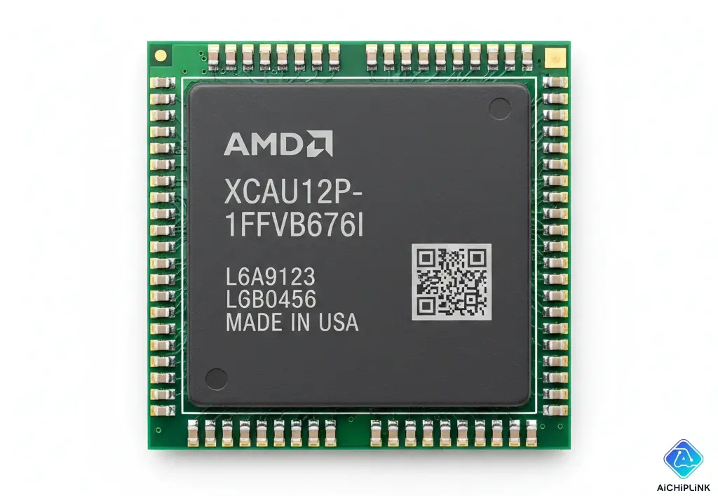
The XCAU15P-1FFVB676I is one of the most capable members of AMD (Xilinx) UltraScale+ families, frequently selected for projects where logic density, memory bandwidth, and I/O flexibility must scale together.
According to recent semiconductor market data, high-end programmable logic devices grew by more than 9% globally in 2024, driven mainly by cloud infrastructure and edge AI platforms. Even more striking, over 60% of new data-plane designs now integrate at least one high-end FPGA to offload real-time workloads.
In this guide, you’ll learn exactly what the XCAU15P-1FFVB676I offers, how its FFVB676 package impacts your PCB design, how it compares to similar devices, and how to source it safely for production.
Let’s walk through specifications, pinout, performance, pricing, and real engineering decisions—step by step.
1.0 What Is XCAU15P-1FFVB676I And Why It Matters
The XCAU15P-1FFVB676I is a high-capacity UltraScale+ FPGA device designed for demanding digital processing platforms.
At its core, it combines:
- High logic density
- Large on-chip memory resources
- High-speed transceivers
- Advanced clocking and power management
What makes this device stand out is its balance between scalable compute fabric and system-level connectivity, making it ideal for:
- High-throughput networking
- Data acquisition
- Image and video processing
- Custom accelerators
For background on FPGA fundamentals, you can refer to the authoritative resource FPGA on Wikipedia: https://en.wikipedia.org/wiki/Field-programmable_gate_array
1.1 UltraScale+ Architecture Explained
The device is built on AMD Xilinx’s UltraScale+ architecture, which introduces:
- Improved logic utilization
- Higher DSP performance per watt
- Better clocking and routing efficiency
Think of the architecture like a city grid. Earlier FPGA families added more buildings, but UltraScale+ redesigned the streets so traffic flows faster—even when the city gets bigger.
Key architectural advantages include:
- Advanced CLB structure
- Dedicated DSP slices for signal processing
- Optimized block RAM and UltraRAM
1.2 Typical Applications And Market Demand
You will most often see XCAU15P-1FFVB676I in:
- High-speed Ethernet switches and routers
- Industrial vision platforms
- Test and measurement equipment
- AI inference and data-preprocessing cards
If you are developing industrial platforms, you may also find this article useful: industrial embedded computing solutions –
2.0 XCAU15P-1FFVB676I Datasheet And Core Specifications
When engineers search for XCAU15P-1FFVB676I datasheet, they usually want one thing: a clear picture of usable resources.
2.1 Logic, DSP And Memory Resources
The device delivers:
- High programmable logic capacity
- Hundreds of DSP slices
- Large internal RAM blocks
In real systems, this translates into:
- Parallel packet processing
- Multi-channel signal pipelines
- On-chip buffering without external memory
Key highlights:
- High logic density FPGA
- Integrated DSP acceleration
- Large on-chip memory resources
For memory interface background, see DDR SDRAM on Wikipedia: https://en.wikipedia.org/wiki/DDR_SDRAM
2.2 High-Speed Transceivers And Interfaces
Modern systems are defined by bandwidth. This device supports:
- Multi-gigabit serial transceivers
- High-speed memory interfaces
- Flexible clocking domains
If you are working on high-speed links, you may want to explore our related guide: high-speed serial interface ICs
3.0 XCAU15P-1FFVB676I Pinout And FFVB676 Package Guide
The XCAU15P-1FFVB676I pinout and package selection directly affect board cost, layer count, and routing risk.
3.1 I/O Bank Structure And Voltage Planning
The device organizes I/O into multiple banks, each with its own supply requirements.
You should plan carefully for:
- I/O bank voltage compatibility
- Differential pair placement
- Shared reference voltages
Design tips:
- Keep bank voltage rails isolated
- Group similar interfaces per bank
- Reserve spare I/O for future expansion
3.2 Mechanical And PCB Footprint Notes
The FFVB676 package:
- Uses a fine-pitch BGA
- Requires controlled impedance routing
- Benefits from blind or buried vias
For many first-time users, this package increases PCB cost by 15–25% compared with mid-pin-count packages.
If you are new to BGA layout, this reference on ball grid array from Wikipedia is helpful: https://en.wikipedia.org/wiki/Ball_grid_array
4.0 Performance, Power And Comparison With XCAU10P
4.1 Power Consumption And Thermal Design
The XCAU15P-1FFVB676I power consumption depends heavily on:
- Toggle rate
- Transceiver usage
- On-chip memory activity
Typical design strategies include:
- Early power estimation using vendor tools
- Power rail segmentation
- Airflow and heat-sink planning
“Thermal margin is not a luxury—it is your production insurance.”
4.2 XCAU15P vs XCAU10P
| Feature | XCAU15P | XCAU10P |
|---|---|---|
| Logic capacity | Higher | Medium |
| DSP resources | More | Fewer |
| Suitable workloads | Heavy data plane | Control + moderate data |
| Power budget | Higher | Lower |
| Typical cost | Higher | Lower |
If your workload is mostly control-oriented, XCAU10P may be enough. But for multi-lane processing, XCAU15P-1FFVB676I offers far more headroom.
5.0 Price, Availability And Sourcing Strategy
[Insert image: FPGA market pricing trend chart – alt="XCAU15P-1FFVB676I market price trend"]
5.1 Market Price And Lead Time
The XCAU15P-1FFVB676I price varies significantly depending on:
- Order volume
- Contract vs spot sourcing
- Regional availability
In 2024–2025, high-end FPGAs typically show:
- Lead times from 16 to 32 weeks
- Volatile spot pricing
To monitor safe sourcing, check our component market insights: electronic component market trends
5.2 Alternatives And Lifecycle Status
The device currently remains in active production.
Common alternatives include:
- Lower-density UltraScale+ parts
- Versal adaptive SoCs (for heterogeneous workloads)
However, migration usually requires:
- New board design
- Software refactoring
- Toolchain updates
6.0 How To Select XCAU15P-1FFVB676I For Your Design
Here is a simple selection checklist:
- Confirm logic and DSP requirements
- Validate FFVB676 package routing capability
- Estimate power and cooling
- Verify interface counts
- Secure supply commitments early
A short practical video walkthrough on UltraScale+ design flow is below.
Conclusion
The XCAU15P-1FFVB676I stands out as a highly capable solution for modern data-centric platforms where performance, scalability, and interface density must coexist in a single programmable device.
More importantly, this FPGA is not just about raw resources. Its real value comes from how efficiently you can translate logic, memory, and transceivers into reliable system throughput—while still keeping thermal and sourcing risks under control.
As networking infrastructure, edge computing, and AI-assisted systems continue to grow through 2025 and beyond, high-capacity programmable logic devices like XCAU15P will remain central to flexible hardware architectures.
If you are planning a new design or need help sourcing this device safely for production, explore our component intelligence platform at https://aichiplink.com and start building a secure, future-proof supply strategy today.

Written by Jack Elliott from AIChipLink.
AIChipLink, one of the fastest-growing global independent electronic components distributors in the world, offers millions of products from thousands of manufacturers, and many of our in-stock parts is available to ship same day.
We mainly source and distribute integrated circuit (IC) products of brands such as Broadcom, Microchip, Texas Instruments, Infineon, NXP, Analog Devices, Qualcomm, Intel, etc., which are widely used in communication & network, telecom, industrial control, new energy and automotive electronics.
Empowered by AI, Linked to the Future. Get started on AIChipLink.com and submit your RFQ online today!
Frequently Asked Questions
What is XCAU15P-1FFVB676I?
The XCAU15P-1FFVB676I is a high-density UltraScale+ FPGA designed for bandwidth-intensive and compute-heavy digital systems.
Is XCAU15P-1FFVB676I suitable for AI acceleration?
Yes. It is commonly used for pre-processing, data movement, and custom acceleration pipelines.
What package does XCAU15P-1FFVB676I use?
It uses the FFVB676 BGA package, which requires high-quality PCB fabrication and controlled impedance routing.
How long is the typical lead time?
Lead time usually ranges from 16 to 32 weeks, depending on supplier allocation and order volume.
What are good alternatives if XCAU15P is unavailable?
Lower-density UltraScale+ devices or Versal adaptive SoCs are typical migration options.