What Is K4B4G1646E-BCNB? The "4G" in the Part Number Does Not Mean What Most People Think It Means
When an engineer encounters K4B4G1646E-BCNB on a BOM for the first time, the most natural reading is "4G memory chip — four gigabytes." This reading is wrong, and the error compounds quickly when someone starts calculating how many chips are needed to hit a target memory capacity. The "4G" in K4B4G1646E-BCNB is 4 gigabit — that is 4,000,000,000 bits, which converts to 512 megabytes (0.5 GB), not four gigabytes.
This unit confusion — gigabit versus gigabyte, a factor of eight difference — is not a niche pedantic concern. It directly determines how many DRAM chips go on a PCB, how the memory controller's address map is configured, and what the total system memory capacity actually is. Four K4B4G1646E-BCNB chips wired in a standard 32-bit wide configuration give 2 GB of total memory, not 16 GB. Getting this wrong at the design stage has cost engineers weeks of rework.
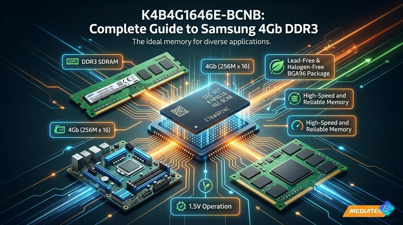
Once the capacity is clear, the rest of the part number decodes into a precise specification: Samsung's 4Gb DDR3 E-die, 256M × 16-bit organization, DDR3-2133 speed grade, 96-ball FBGA package. Each of those fields carries specific design implications for the PCB layout, power delivery, and memory controller initialization. This guide works through all of them.
1.0 Full Part Number Decoded: K4B4G1646E-BCNB
Samsung's DRAM part numbers are fully specified identifiers. Every character group carries meaning:
K — Samsung semiconductor product prefix (K = memory device)
4 — Product type: 4 = DRAM
B — DRAM sub-type: B = DDR SDRAM family
4G — Density: 4 gigabit (4Gb) — this is the most frequently misread field. "4G" = four giga-bit, not byte. 4 Gb = 512 MB = 0.5 GB. To get to gigabytes: divide by 8.
16 — Data bus width: 16 bits (x16 organization — the chip presents 16 data lines, DQ0–DQ15)
4 — Internal organization code (maps to 8 banks in the DDR3 architecture for this density)
6 — Generation / feature code within the DDR3 B-series
E — Die revision: E-die — Samsung uses alphabetic die codes to identify specific silicon generations within a product family. The E-die for the 4Gb DDR3 is associated with the higher speed grades (DDR3-2133). Earlier die revisions (B-die, etc.) exist for lower speed grades of the same nominal capacity.
-BC — Speed bin group prefix: BC = the group of speed bins supporting DDR3-1600 through DDR3-2133 for this die
NB — Speed grade suffix within the BC group:
- BCK0 = DDR3-1600 (11-11-11), tCK(min) = 1.25 ns
- BCMA = DDR3-1866 (13-13-13), tCK(min) = 1.071 ns
- BCNB = DDR3-2133 (14-14-14), tCK(min) = 0.938 ns
The two characters NB thus encode the specific speed grade: DDR3-2133, CAS latency 14, maximum clock frequency 1066 MHz (2133 MT/s with DDR double-pumping).
Full ordering description: Samsung 4Gb DDR3 SDRAM, E-die, 256M × 16-bit organization, DDR3-2133 speed grade, 96-ball FBGA package, 0°C to 95°C operating temperature.
2.0 Specifications and What They Actually Mean
From Samsung's K4B4G1646E datasheet (Rev. 1.0/1.1):
Capacity and organization:
- Total capacity: 4 Gb (4,294,967,296 bits)
- In usable bytes: 512 MB per chip
- Organization: 32M rows × 16 DQ bits × 8 banks = 4 Gb
- Address mapping: Row address A0–A12 (13 bits = 8,192 rows per bank), Column address A0–A9 (10 bits = 1,024 columns), Bank address BA0–BA2 (3 bits = 8 banks)
- Page size: 2 KB (the amount of data activated from the array per ACTIVE command in one bank)
Speed grade (BCNB = DDR3-2133):
- Maximum data rate: 2133 Mb/s per pin (MT/s)
- Clock frequency: 1066 MHz maximum
- tCK(min): 0.938 ns
- CAS latency (CL): 14 clock cycles at DDR3-2133
- tRCD (RAS to CAS delay): 14 ns minimum
- tRP (Row Precharge time): 14 ns minimum
- tRAS (Active to Precharge minimum): 33 ns minimum
The device also operates at lower speeds (all DDR3-800 through DDR3-2133 are supported, as lower speeds are a subset of the higher-speed timing):
| Speed Grade | tCK(min) | CL | tRCD | tRP |
|---|---|---|---|---|
| DDR3-800 | 2.5 ns | 6 | 15 ns | 15 ns |
| DDR3-1066 | 1.875 ns | 7 | 13.1 ns | 13.1 ns |
| DDR3-1333 | 1.5 ns | 9 | 13.5 ns | 13.5 ns |
| DDR3-1600 | 1.25 ns | 11 | 13.75 ns | 13.75 ns |
| DDR3-1866 | 1.071 ns | 13 | 13.91 ns | 13.91 ns |
| DDR3-2133 | 0.938 ns | 14 | 13.09 ns | 13.09 ns |
Interface:
- DQ bus width: 16 bits (x16)
- Differential clock: CK / CK# (single differential pair)
- Data strobes: UDQS/UDQS# (upper byte DQ8–DQ15), LDQS/LDQS# (lower byte DQ0–DQ7)
- Data masks: UDM (upper byte), LDM (lower byte)
- On Die Termination (ODT): Enabled via mode register; applies to DQ, DQS, DQS#, and DM signals
Power:
- VDD: 1.5V (1.425V to 1.575V) — standard DDR3 voltage
- VDDQ: 1.5V (same as VDD for DDR3; this part is DDR3, not DDR3L)
- IDD4R (peak read current, DDR3-2133): approximately 200–250 mA per chip (check datasheet IDD table for exact values at the operating speed)
- IDD3N (active standby): approximately 40–60 mA per chip
Package:
- 96-ball FBGA (Fine-pitch Ball Grid Array)
- Ball pitch: 0.8 mm
- Body dimensions: approximately 9 mm × 9 mm × 1.0 mm
3.0 The Capacity Math: 4Gb, 256Mx16, and What You Can Build With It
This is the section that prevents the most common design error with this part.
Starting from the part number:
4Gb capacity, x16 data bus width.
One chip = 4 Gb = 4,096 Mb = 512 MB = 0.5 GB.
What "256Mx16" means:
The chip is internally organized as 256 million addresses, each address storing 16 bits. 256M × 16 bits = 256M × 2 bytes = 512 MB. The "256M" in the organization refers to addressable locations (row × column × bank), not megabytes.
Building a 32-bit wide DDR3 memory interface:
Most embedded processors (Allwinner, Rockchip, NXP i.MX, Broadcom BCM series) implement a 32-bit DDR3 interface. One x16 chip only provides 16 data bits. Two x16 chips side by side, with their DQ[15:0] buses connected to the controller's DQ[15:0] and DQ[31:16] respectively, give a 32-bit wide interface. Total capacity with two chips: 2 × 512 MB = 1 GB.
Building a 16-bit wide interface:
Some cost-optimized embedded designs use a 16-bit DDR3 interface. One K4B4G1646E-BCNB chip provides the complete 16-bit bus. Total capacity: 512 MB.
Building higher capacities:
| Configuration | Chips | DQ Width | Total Capacity |
|---|---|---|---|
| 1 chip | 1× K4B4G1646E-BCNB | 16-bit | 512 MB |
| 2 chips | 2× K4B4G1646E-BCNB | 32-bit | 1 GB |
| 4 chips | 4× K4B4G1646E-BCNB | 32-bit, 2 ranks | 2 GB |
| 8 chips | 8× K4B4G1646E-BCNB | 64-bit (ECC) | 4 GB |
For a 64-bit wide interface (standard for desktop DIMMs), 4 chips provide 64-bit width and 2 GB; 8 chips provide 64-bit width with ECC via an additional x8 chip, or 4 GB with two 4-chip ranks.
4.0 Real Circuit Application: How This Chip Connects to a Memory Controller
Typical embedded system usage:
The K4B4G1646E-BCNB is widely used in:
- Single-board computers (Raspberry Pi Compute Module 3+, Orange Pi, NanoPi variants, BeagleBone derivatives)
- IoT gateway modules
- Industrial HMI controllers
- Set-top boxes and smart TV mainboards
- Embedded vision systems
In a Raspberry Pi Compute Module 3+ configuration, two K4B4G1646E or similar 4Gb DDR3 chips provide the 1 GB LPDDR2 — though the Pi uses LPDDR2 not DDR3, this illustrates the physical scale: two BGA chips totaling under 2 cm² of PCB area providing the entire system memory.
Signal groups from one chip (x16 configuration):
- DQ[15:0]: 16 bidirectional data lines
- UDQS / UDQS#: Upper byte data strobe (differential, DQ8–DQ15)
- LDQS / LDQS#: Lower byte data strobe (differential, DQ0–DQ7)
- UDM / LDM: Data mask (upper and lower byte)
- CK / CK#: Differential clock input
- CKE: Clock enable
- CS#: Chip select
- RAS# / CAS# / WE#: Command signals
- A[12:0]: Address bus (13-bit row, 10-bit column, multiplexed)
- BA[2:0]: Bank address
- ODT: On-die termination control
- RESET#: Asynchronous reset
- VDD / VDDQ / VSS / VSSQ: Power and ground (multiple balls each)
5.0 Five Misconceptions About This Part
Misconception 1: "4G in the part number means 4GB of memory"
Covered in detail above — this is the single most common and most consequential error. 4G = 4 gigabit = 512 megabytes. Any design calculation using 4 GB for this chip will produce a memory map and chip count that is off by a factor of eight.
Misconception 2: "DDR3-2133 requires a 2133 MHz clock"
DDR3-2133 achieves 2133 megabytes per second per pin (MT/s) through Double Data Rate — the bus transfers data on both the rising and falling edges of the clock. The actual clock frequency is half the data rate: 1066 MHz. The clock signal running on the CK/CK# differential pair is 1066 MHz, not 2133 MHz. This distinction matters for PCB trace length matching calculations and for oscilloscope verification of the clock signal.
Misconception 3: "K4B4G1646E-BCNB is DDR3L (low voltage)"
The BCNB part is DDR3 at 1.5V — not DDR3L. DDR3L (Low voltage) operates at 1.35V and carries a different Samsung part number series (the DDR3L E-die has its own K4B4G1646E-series designations but with different suffix patterns and is specified with VDD = 1.35V). Applying 1.5V to a DDR3L part is within spec; applying 1.35V to a DDR3 part may cause unreliable operation — but the specific voltage specification of the component on the BOM should be verified. If the design requires 1.35V operation (for power budget reasons), explicitly select the DDR3L variant.
Misconception 4: "CAS latency 14 means this chip is slow compared to older DDR3 with CL9"
CAS latency is measured in clock cycles, not nanoseconds. At DDR3-2133 with tCK = 0.938 ns, CL14 represents an absolute latency of 14 × 0.938 ns = 13.1 ns. At DDR3-1333 with CL9 (a "faster" CAS latency number), the absolute latency is 9 × 1.5 ns = 13.5 ns — slightly longer. Higher CL numbers at higher frequencies do not necessarily indicate longer absolute memory latency. The relevant metric for system performance is the absolute time in nanoseconds, not the CL number in isolation.
Misconception 5: "All K4B4G1646E variants are interchangeable on the same PCB"
The BCK0 (DDR3-1600), BCMA (DDR3-1866), and BCNB (DDR3-2133) variants share the same package and are pin-compatible. A BCNB can replace a BCK0 on the same PCB footprint. However, the memory controller must be initialized with timing parameters matching the actual installed chip speed — not the speed grade it might have run before. If BCNB chips are installed in a system configured for BCK0 timing, the system will run at the slower DDR3-1600 rate (which is fine). If BCK0 chips are installed in a system expecting DDR3-2133, the chips cannot meet the 0.938 ns cycle time requirement and the system will be unstable. Always match controller initialization to the installed chip's rated speed grade, or stay at or below the chip's rated speed.
6.0 PCB Design Notes: Layout, Decoupling, and ODT
PCB stack and trace impedance:
DDR3 at 2133 MT/s is a high-speed interface requiring controlled impedance PCB traces. Target single-ended trace impedance of 40–50 Ω (for DQ, DM, address, command) and differential impedance of 80–100 Ω for the CK/CK# and DQS/DQS# pairs. This requires at minimum a 4-layer PCB with defined dielectric thickness between signal and reference plane layers.
Trace length matching:
Within a DQ byte group (DQ0–DQ7 with LDQS, or DQ8–DQ15 with UDQS), match trace lengths to within ±25 ps (approximately ±4 mm on FR4). Between byte groups and the clock, match to within ±100 ps (±15 mm). Address and command signals should be matched to ±200 ps of the clock (±30 mm). These tolerances ensure adequate setup/hold margin at DDR3-2133 speeds.
Decoupling capacitors:
Place 100 nF X5R/X7R ceramic decoupling capacitors on every VDD and VDDQ ball pair, within 2 mm of the chip. The 96-ball FBGA has multiple VDD/VSS and VDDQ/VSSQ power/ground balls distributed around the package — each needs its own dedicated 100 nF bypass. Add 4.7–10 µF bulk capacitance per 512 MB chip on the board-level power supply.
On Die Termination (ODT):
DDR3's ODT feature provides termination resistance inside the DRAM chip itself, eliminating the need for discrete series termination resistors on the data bus in most designs. Enable ODT through mode register MR1 settings during initialization. The ODT impedance (typically 40 Ω, 60 Ω, or 120 Ω) should be selected based on the PCB trace impedance and the signal integrity simulation results for the specific layout. For typical embedded designs at 1–2 GB capacity (2–4 chips, moderate trace lengths), 60 Ω ODT is a common starting point.
FBGA96 footprint:
The 96-ball FBGA uses 0.8 mm ball pitch — manageable on a standard 4-layer PCB using 0.4 mm via drill diameter with dogbone via escaping. Unlike the very fine 0.5 mm BGA pitch of larger FPGAs, the DDR3 0.8 mm pitch does not require advanced PCB fabrication capabilities.
7.0 Real Questions from Hardware Designers
Q: I am designing a 1 GB DDR3 memory subsystem using two K4B4G1646E-BCNB chips with a 32-bit controller. Should I use one chip select or two?
A: For two chips wired in a standard 32-bit configuration (chips side by side, each providing 16 bits of the 32-bit bus, both sharing the same address/command/clock signals), you can use a single chip select (CS#) signal driving both chips. This creates a single-rank 32-bit × 512M configuration presenting 1 GB to the memory controller as one contiguous rank. The controller sees 1 GB of single-rank memory at 32-bit width. If you wanted to expand to 2 GB by adding a second pair of chips, you would add a second CS# signal for the second pair (creating a dual-rank configuration), and the controller would address the two ranks separately. For most embedded designs where 1 GB is the target, single chip select with two chips is the standard approach.
Q: The datasheet shows DDR3-2133 as the maximum speed. My processor's DDR3 controller only supports up to DDR3-1600. Can I use K4B4G1646E-BCNB at DDR3-1600?
A: Yes. A DDR3-2133-rated chip can always run at lower speeds — DDR3-1600, DDR3-1333, or any lower speed grade. The BCNB part is guaranteed to meet DDR3-2133 timing, which implicitly guarantees it meets all lower speed grades (a faster chip operating slower is always within spec). Configure your memory controller to DDR3-1600 timing (CL11, tRCD = 13.75 ns, etc.), and the K4B4G1646E-BCNB chips will operate correctly at those settings. You are simply using a chip that could run faster than your controller allows — no issue. The alternative approach is to use the BCK0 (DDR3-1600) variant, which is typically lower cost if you do not need DDR3-2133 capability.
Q: How do I verify that received K4B4G1646E-BCNB chips are genuine Samsung parts and not counterfeits?
A: Counterfeit DDR3 chips are common in the secondary market, typically as lower-capacity chips (256 Mb or 512 Mb) relabeled as 4Gb parts. Physical verification: examine the package marking under magnification — genuine Samsung FBGA chips have consistent, clean laser-marked text on the top surface. Functional verification: write a known pattern to every address in the chip's full 512 MB address space and read it back; counterfeit chips with lower actual capacity will show data aliasing where high addresses repeat the data written to low addresses. Use a memory test tool (memtester on Linux, or a bare-metal memory validation routine for embedded systems) that exercises the full address range. In a Linux system, memtool or a simple write-then-read-back test across the entire memory range is the most reliable functional counterfeit detection method.
8.0 Quick Reference Card
Part Number Decode:
| Field | Value | Meaning |
|---|---|---|
| K4B | K4B | Samsung DRAM device |
| 4G | 4G | 4 gigabit = 512 MB ≠ 4 GB |
| 16 | 16 | x16 data bus (16 DQ pins) |
| 4 | 4 | 8-bank organization code |
| 6E | 6E | DDR3 generation, E-die |
| BC | BC | Speed bin group (DDR3-1600–2133) |
| NB | NB | DDR3-2133 speed grade (14-14-14) |
The Capacity Conversion Table:
| Part says | Actual capacity | Why |
|---|---|---|
| 4G | 512 MB | 4 Gb ÷ 8 bits/byte = 0.5 GB |
| 4G × 2 chips | 1 GB | 32-bit interface |
| 4G × 4 chips | 2 GB | 32-bit, dual rank |
DDR3-2133 Key Timing (BCNB):
| Parameter | Value |
|---|---|
| tCK(min) | 0.938 ns |
| Clock frequency | 1066 MHz (not 2133 MHz) |
| CAS Latency | 14 clock cycles |
| tRCD | 13.09 ns |
| tRP | 13.09 ns |
| VDD / VDDQ | 1.5V (not 1.35V — that is DDR3L) |
Speed Grade Variants of K4B4G1646E:
| Suffix | Speed | CL | Clock | Note |
|---|---|---|---|---|
| BCK0 | DDR3-1600 | 11 | 800 MHz | Most common |
| BCMA | DDR3-1866 | 13 | 933 MHz | Mid-tier |
| BCNB | DDR3-2133 | 14 | 1066 MHz | Highest speed |
For sourcing Samsung K4B4G1646E-BCNB DDR3 SDRAM with verified authenticity and competitive pricing, visit aichiplink.com.

Written by Jack Elliott from AIChipLink.
AIChipLink, one of the fastest-growing global independent electronic components distributors in the world, offers millions of products from thousands of manufacturers, and many of our in-stock parts is available to ship same day.
We mainly source and distribute integrated circuit (IC) products of brands such as Broadcom, Microchip, Texas Instruments, Infineon, NXP, Analog Devices, Qualcomm, Intel, etc., which are widely used in communication & network, telecom, industrial control, new energy and automotive electronics.
Empowered by AI, Linked to the Future. Get started on AIChipLink and submit your RFQ online today!
Frequently Asked Questions
What does “4G” mean in K4B4G1646E-BCNB?
In K4B4G1646E-BCNB, the “4G” refers to 4 gigabits (Gb), not gigabytes (GB). This equals 512 MB per chip, since 1 byte = 8 bits. Misinterpreting this is a common mistake that leads to incorrect memory capacity planning in system design.
Can K4B4G1646E-BCNB run at lower speeds than DDR3-2133?
Yes, although K4B4G1646E-BCNB is rated for DDR3-2133, it is fully backward-compatible with lower speeds such as DDR3-1600 or DDR3-1333. The memory controller simply initializes the device with relaxed timing parameters, allowing stable operation at reduced frequencies.
Is K4B4G1646E-BCNB DDR3 or DDR3L?
K4B4G1646E-BCNB is a standard DDR3 device operating at 1.5V, not DDR3L (1.35V). Using incorrect voltage can lead to instability or failure, so designers must ensure the power rail matches the device specification.
How many chips are needed to build 1GB or 2GB memory?
Each K4B4G1646E-BCNB chip provides 512 MB, so a typical 1GB system uses two chips (x16 + x16 = 32-bit bus), while 2GB requires four chips in a dual-rank configuration. The total depends on both capacity and bus width requirements of the memory controller.
How can I detect counterfeit K4B4G1646E-BCNB chips?
Counterfeit detection usually involves both visual inspection and functional testing. Engineers verify markings on the package and run full memory tests across the address space; fake chips often show data mirroring or reduced capacity when accessing higher memory regions.


