Table of Contents
- 1.0 What is the XC4VLX100-10FFG1148C? An Introduction
- 2.0 Key Technical Specifications (Datasheet Deep Dive)
- 3.0 Core Architectural Features of the Virtex-4 Family
- 4.0 Applications, Programming, and Design Considerations
For engineers maintaining long-lifecycle systems or designers seeking powerful, field-proven FPGAs, the Xilinx Virtex-4 family remains a significant landmark in programmable logic. The XC4VLX100-10FFG1148C is a formidable member of this family, offering a substantial array of logic resources optimized for complex digital designs. While newer generations have emerged, understanding the capabilities of this 90nm workhorse is crucial for supporting existing applications in industrial, communications, and defense sectors.
This technical guide provides a comprehensive overview of the XC4VLX100-10FFG1148C, breaking down its datasheet specifications, core architectural features, and primary applications to serve as an essential resource for engineers and designers.
1.0 What is the XC4VLX100-10FFG1148C? An Introduction
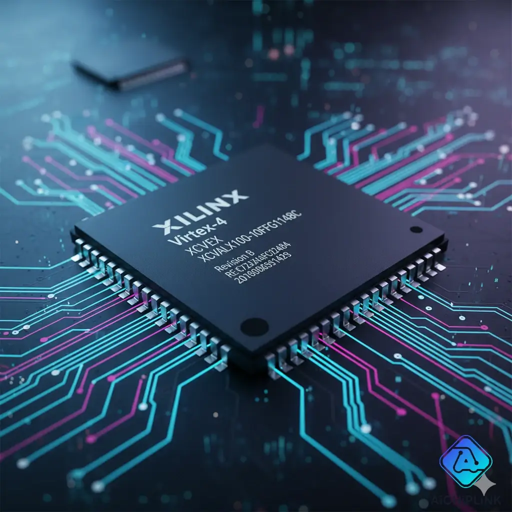
The XC4VLX100-10FFG1148C is a high-performance Field-Programmable Gate Array (FPGA) manufactured by Xilinx (now AMD). It is built on a 90nm copper CMOS process and is designed to serve as a powerful alternative to ASIC technology by providing extensive programmable logic capabilities.
1.1 Core Definition: A Virtex-4 LX Family FPGA
This specific chip is part of the Virtex-4 LX platform, one of three families in the Virtex-4 lineup. The LX platform is optimized for logic-intensive applications, offering the highest logic density and a cost-effective balance of high-performance logic and I/O. This distinguishes it from the SX family (for DSP) and the FX family (for embedded processing and serial connectivity).
1.2 Understanding the Part Number
The part number XC4VLX100-10FFG1148C provides key information about the device:
- XC4V: Identifies the device as part of the Virtex-4 family.
- LX: Specifies the logic-optimized LX platform.
- 100: Refers to the device's logic density, indicating approximately 100,000 logic cells. (The precise number is 110,592) .
- -10: Denotes the speed grade of the device.
- FFG1148: Describes the package type—a 1148-ball Fine-Pitch BGA package.
- C: Indicates the commercial temperature range (0°C to 85°C).
2.0 Key Technical Specifications (Datasheet Deep Dive)
The datasheet reveals the powerful capabilities of this FPGA. The following tables summarize the core specifications.
2.1 Logic and Memory Resources
| Specification | Value | Source(s) |
|---|---|---|
| Number of Logic Elements/Cells | 110,592 | |
| Number of LABs/CLBs | 12,288 | |
| Total RAM Bits | 4,423,680 | |
| Distributed RAM | 768 kbit | |
| Embedded Block RAM (EBR) | 4,320 kbit |
2.2 Performance and I/O Capabilities
| Specification | Value | Source(s) |
|---|---|---|
| Maximum Operating Frequency | 500 MHz | |
| Number of I/O | 768 | |
| XtremeDSP™ Slices | 640 | |
| Digital Clock Managers (DCMs) | 8 |
2.3 Operating Conditions and Package Details
| Specification | Value | Source(s) |
|---|---|---|
| Voltage - Supply (Core) | 1.14V ~ 1.26V (1.2V Nominal) | |
| I/O Voltage Operation | 1.5V to 3.3V | |
| Operating Temperature (Commercial) | 0°C ~ 85°C | |
| Mounting Type | Surface Mount (SMD/SMT) | |
| Package / Case | 1148-BBGA, FCBGA | |
| Supplier Device Package | 1148-FCPBGA (35x35) |
3.0 Core Architectural Features of the Virtex-4 Family
The Virtex-4 family introduced several architectural enhancements that made it a powerful platform.
3.1 ASMBL™ (Advanced Silicon Modular Block) Architecture
This architecture combines a wide variety of flexible features and hard-IP core blocks, enhancing design capabilities and making it a strong alternative to ASIC technology.
3.2 Flexible Logic Resources and XtremeDSP™ Slices
The device contains an abundance of flexible logic resources with up to 200,000 logic cells in the family. A key feature is the inclusion of dedicated XtremeDSP slices. These are high-performance DSP blocks that include an 18 x 18 signed multiplier, a built-in accumulator, and an adder/subtracter, capable of operating at up to 500 MHz.
3.3 High-Speed Clock Management (DCMs)
The Virtex-4 family includes up to twenty Digital Clock Manager (DCM) modules for precision clock deskew, phase shifting, and flexible frequency synthesis. These blocks, along with Phase-Matched Clock Dividers (PMCDs), enable robust and high-speed clocking schemes.
3.4 SelectIO™ Technology
This feature provides a wide range of I/O standard compatibility, from 1.5V to 3.3V. It also includes features like Digitally Controlled Impedance (DCI) for active termination and built-in ChipSync™ technology to simplify the design of source-synchronous interfaces.
4.0 Applications, Programming, and Design Considerations
The combination of high logic density and I/O count makes this FPGA ideal for demanding digital logic implementations.
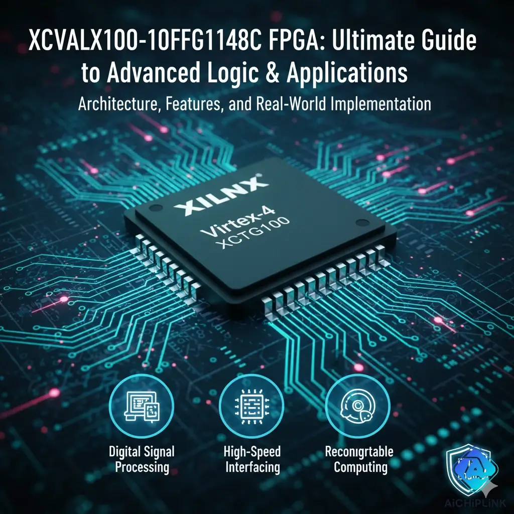
4.1 Common Applications for the XC4VLX100-10FFG1148C
With its large logic capacity and embedded memory, the XC4VLX100-10FFG1148C is well-suited for a variety of high-performance tasks:
- Digital Signal Processing (DSP) Systems: Ideal for implementing custom processing pipelines for applications like image processing, radar systems, and advanced filtering.
- Communications and Networking: Suitable for managing complex protocols and high-bandwidth data streams in switches, routers, and interface bridges.
- Embedded System Acceleration: Used to offload tasks from software to hardware, accelerating functions like protocol handling and bus management to improve system responsiveness.
- High-Speed Data Acquisition: Excels in instrumentation and scientific equipment that require rapid data capture and real-time processing.
4.2 Programming and Development Tools
- Software: The Virtex-4 family is primarily supported by the Xilinx ISE® Design Suite. For designs involving embedded processors, the Xilinx Embedded Developers Kit (EDK®) is also used.
- Programming: The device is configured via standard FPGA interfaces like JTAG. The bitstream can be secured with AES encryption.
The XC4VLX100-10FFG1148C represents a powerful and capable FPGA from the mature Virtex-4 family. Its substantial logic resources, flexible I/O, and dedicated DSP and clocking blocks make it a robust choice for complex, high-performance digital logic designs. While newer FPGA families offer higher performance and lower power consumption, understanding the architecture and capabilities of the Virtex-4 series is essential for maintaining and developing for a wide range of long-lifecycle systems across multiple industries.
Looking for the XC4VLX100-10FFG1148C or other Virtex-family FPGAs? Explore our inventory of programmable logic ICs at aichiplink.com to find the components for your legacy and new designs today!

Written by Jack Elliott from AIChipLink.
AIChipLink, one of the fastest-growing global independent electronic components distributors in the world, offers millions of products from thousands of manufacturers, and many of our in-stock parts is available to ship same day.
We mainly source and distribute integrated circuit (IC) products of brands such as Broadcom, Microchip, Texas Instruments, Infineon, NXP, Analog Devices, Qualcomm, Intel, etc., which are widely used in communication & network, telecom, industrial control, new energy and automotive electronics.
Empowered by AI, Linked to the Future. Get started on AIChipLink.com and submit your RFQ online today!
Frequently Asked Questions
What is the XC4VLX100-10FFG1148C?
The XC4VLX100-10FFG1148C is a high-performance Field-Programmable Gate Array (FPGA) from the Xilinx (now AMD) Virtex-4 LX family. It features 110,592 logic cells, over 4.4 Mbit of total RAM, 768 user I/O pins, and is housed in an 1148-pin FCBGA package. It is designed for logic-intensive applications.
What does the 'LX' in Virtex-4 LX stand for?
The 'LX' in the Virtex-4 LX platform stands for 'Logic-intensive'. This family of Virtex-4 FPGAs was optimized to provide the highest logic density and a large number of I/Os for general-purpose, high-performance logic applications.
What is the maximum frequency of the XC4VLX100-10FFG1148C?
The XC4VLX100-10FFG1148C supports a maximum operating frequency of up to 500 MHz.
What is the core voltage for this FPGA?
The core voltage (VCCINT) for the XC4VLX100-10FFG1148C is a nominal 1.2V, with a recommended operating range of 1.14V to 1.26V.
What kind of applications is the Virtex-4 LX family best for?
The Virtex-4 LX platform is optimized for general logic applications that are high-density and I/O intensive. This includes tasks in digital signal processing, communications infrastructure, and high-speed data acquisition.