Exploring the TTL NAND Gate Circuit and Its Internal Operation
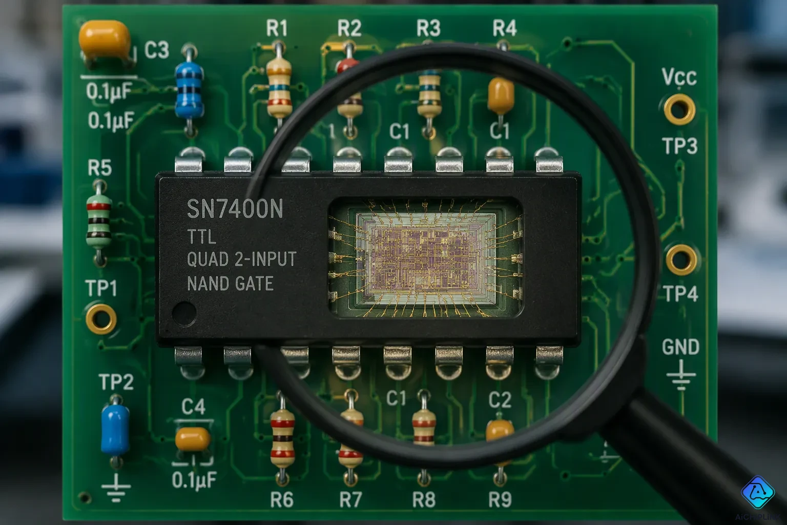
A TTL NAND gate uses a multi-emitter input transistor Q1, a phase-splitter Q2, and a totem-pole output stage Q3/Q4. This circuit gives a LOW output only when all inputs are HIGH. Any input LOW makes the output HIGH. Think of Q1 as your input sensor and Q2 as your traffic controller. TTL stands for Transistor-Transistor Logic. You will trace the whole operation through this simple circuit. The TTL NAND gate works with four transistors and one diode. You can compare TTL NAND and AND gates by their output conditions. The input transistor detects each signal. Your understanding of this circuit grows with each step. This NAND circuit responds predictably to every input mix. TTL NAND and AND gates share similar structures. The TTL NAND and AND gates differ in output logic. This TTL NAND gate circuit gives you clear, reliable logic behavior. You will master this TTL NAND gate operation quickly.
Key Takeaways
-
A TTL NAND gate sends out a LOW signal only when every input is HIGH; if any input is LOW, it forces the output to go HIGH.
-
The multi-emitter transistor Q1 checks the inputs, and phase-splitter Q2 manages the totem-pole output stage for quick, dependable switching.
-
The totem-pole output uses active pull-up and pull-down paths, so it gives clean voltage levels and about 9 ns propagation delay.
-
TTL logic levels are 0–0.8 V for LOW and 2–5 V for HIGH, giving noise margin for steady work.
TTL NAND Gate Logic: Truth Table and Voltage Levels
Before you trace the internal operation of this circuit, you need a clear picture of what the TTL NAND gate does at its output. The nand gate truth table shows every possible input combination and the resulting output. For a two-input ttl nand gate, you have four states to consider. When both inputs are high, the output drops LOW. Any other combination—00, 01, or 10—produces a HIGH output.
Two-Input NAND Truth Table and Boolean Equation
The truth table for this gate follows a simple pattern. You can think of a NAND gate as an and gate followed by a not gate. First, the AND operation checks if both inputs are high. Then, the NOT operation flips that result. So when both inputs are high, the AND part gives you a HIGH signal, but the NOT part inverts it to LOW.
The Boolean expression for a two-input NAND gate is X = (A . B)' — the complement of the logical multiplication of the inputs.
This expression means you multiply A and B together using AND logic, then apply inversion to get the final output. The NAND operator is also known as the Sheffer Stroke function, denoted as A|B or A↑B. This single function holds special importance because you can build any other logic gate using only NAND gates.
| Input A | Input B | Output X |
|---|---|---|
| 0 | 0 | 1 |
| 0 | 1 | 1 |
| 1 | 0 | 1 |
| 1 | 1 | 0 |
This truth table shows you exactly what to expect from the circuit. Only one row produces a LOW output, and that row requires both inputs to sit at logic HIGH.
TTL Levels: LOW and HIGH
TTL operates with specific voltage boundaries that define logic states. Transistor-transistor logic uses these thresholds to distinguish between a binary 0 and a binary 1. The output voltage from your circuit must fall within these ranges for proper operation.
| Logic State | Voltage Range |
|---|---|
| Logic LOW (0) | 0 – 0.8 V |
| Logic HIGH (1) | 2 – 5 V |
Any voltage below 0.8 V counts as logic LOW. Any voltage above 2 V counts as logic HIGH. According to the SN74LS00 datasheet, a logic '1' input must be higher than 2V, and a logic '0' input must be lower than 0.8V.
These boundaries matter because they give you a safety margin against noise. When you compare ttl nand and and gates, you see they share these same voltage levels. The difference lies in their output logic behavior. Understanding these thresholds helps you predict how the circuit responds in real applications.
Inside the TTL NAND Gate Circuit
The standard two-input TTL NAND gate circuit uses four npn transistors labeled Q1 through Q4, one diode D1, and several resistors. You can trace the signal path through three distinct stages. The input stage uses Q1, the phase-splitting stage uses Q2, and the output stage uses Q3 and Q4 together. Each stage has a specific job in the overall operation.
Multi-Emitter Transistor Q1 and Phase-Splitter Q2
Q1 is a multiple-emitter transistor, meaning it has one collector but two separate emitters. Each emitter connects to one logic input. This design lets Q1 sense both input signals simultaneously. The multiple-emitter input transistor acts as a current-steering switch rather than a normal amplifying transistor. Its equivalent circuit behaves like a two-way switch with one path to the input emitters and another path to the collector.
When any input goes LOW, current from resistor R1 flows out through that input emitter. This forward-biases the base-emitter junction of Q1. The current then flows to ground through the low input, starving Q2 of base drive. Q2 turns off completely. When both inputs go HIGH, the base-emitter junctions cannot conduct because both emitters sit at the same high potential. Instead, current from R1 flows backward through Q1's collector into the base of Q2. This turns Q2 on.
Q2 serves as the phase-splitting transistor. Its collector and emitter connect to the bases of Q3 and Q4 respectively. This arrangement ensures Q3 and Q4 operate in antiphase, meaning they never conduct at the same time. When Q2 turns on, its collector voltage drops and its emitter voltage rises. When Q2 turns off, the opposite happens. This phase-splitting stage creates the two complementary control signals needed for the output stage.
Totem-Pole Output Q3/Q4 and Diode D1
Q3 and Q4 form the totem-pole output stage, also called a push-pull pair. Q3 connects to VCC through resistor R4, while Q4 connects to ground. This configuration allows one output transistor to actively pull the output HIGH while the other pulls it LOW. The push-pull action reduces transition time and improves switching speed.
Diode D1 sits in series with Q3's collector and the output node. This diode raises the effective turn-on voltage of Q4. The voltage offset guarantees that Q4 turns off before Q3 turns fully on during transitions. Without D1, both output transistors could conduct simultaneously, creating a shoot-through current that wastes power and generates heat.
When both inputs go HIGH, Q2 turns on, which drives Q3 off and Q4 on. The output connects to ground through Q4, producing a LOW output. D1 prevents Q3 from conducting when the output sits LOW. When any input goes LOW, Q2 turns off, which turns Q3 on and Q4 off. The output connects to VCC through Q3 and R4, producing a HIGH output.
The ttl nand gate circuit diagram shows these connections clearly. You can see how Q1's collector feeds Q2's base, and how Q2's collector and emitter drive Q3 and Q4. The diode D1 sits between Q3 and the output node. This arrangement gives you fast, reliable switching without excessive power consumption.
The operation of this circuit depends entirely on the input transistors and the phase-splitting transistor making the right decisions. The output stage simply responds to those decisions. When you compare ttl nand and and gates, you see they share similar input structures but differ in output logic. The inversion happens at the output stage, where the totem-pole pair flips the AND result. This inversion gives you the NAND behavior you expect from the truth table.
TTL NAND Gate Operation by Input State
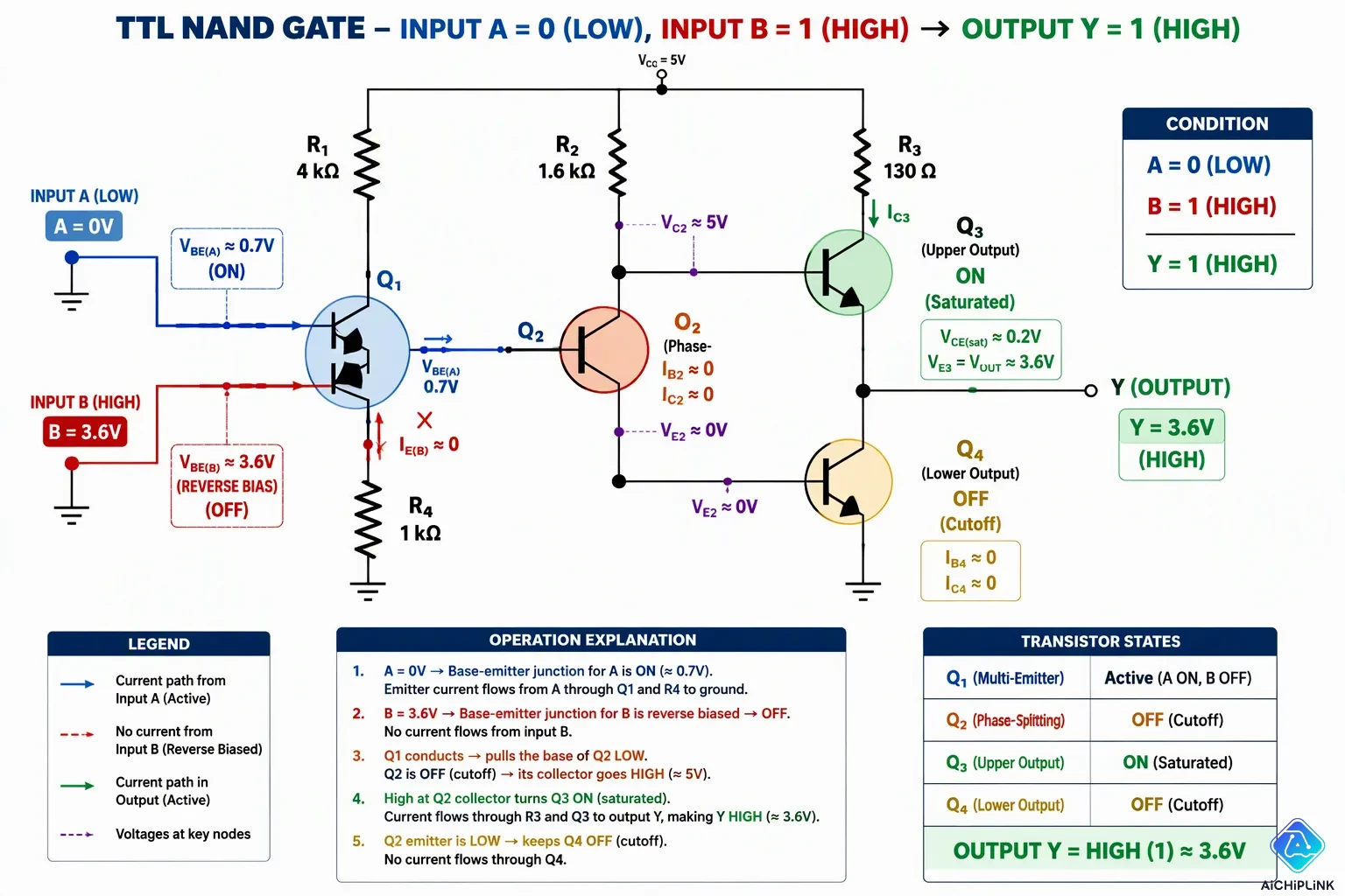
Now you will follow the full operation of this circuit through its two main input conditions. Each condition gives a clear output based on how the transistors behave. You will see how the input stage makes the first choice, how the phase-splitting transistor reacts, and how the output stage gives the final result.
Any Input LOW: Q2 Off and Output HIGH
Think about a case where input A is LOW and input B is HIGH. This is one of the three input states that give a HIGH output. The action starts at the multi-emitter transistor Q1. When input A goes LOW, the base-emitter junction for that input turns on. Current from resistor R1 flows out through that emitter and into the LOW input. This current path pulls Q1's base voltage down to about 0.7 V above the LOW input level.
This turned-on base-emitter junction takes the current that would normally drive Q2. The phase-splitting transistor Q2 loses its base drive completely. With no base current, Q2 shuts off. Its collector voltage rises toward VCC, and its emitter voltage falls to ground. These two voltage changes create the opposite signals needed for the output stage.
The output stage reacts to Q2 being off. Q3, the upper output transistor, gets base drive through resistor R4. Q3 turns on and links the output node to VCC through its collector-emitter path. At the same time, Q4, the lower output transistor, gets no base drive because Q2's emitter sits at ground. Q4 stays off. The output node now sits at a HIGH voltage, about 3.6 V in standard TTL circuits.
You can check this with the truth table row where A is 0 and B is 1. The output Y is 1, which confirms that any input LOW gives a HIGH output. The same thing happens when input B goes LOW and input A stays HIGH. The multi-emitter design makes sure that any LOW input triggers the same response. The input stage sees the LOW signal, the phase-splitting transistor turns off, and the output stage gives a HIGH result.
All Inputs HIGH: Q2 On and Output LOW
Now look at the case where both inputs are HIGH. This single condition gives the LOW output that defines the NAND operation. When both inputs are high, the base-emitter junctions of Q1 cannot turn on. Both emitters sit at the same HIGH voltage, so no current flows through either input path. Instead, current from resistor R1 flows backward through Q1's collector into the base of Q2.
This reverse current path turns on the base-collector junction of Q1. The current reaches Q2's base and turns it on. Q2 conducts and enters saturation. Its collector voltage drops to about 0.2 V above ground, while its emitter voltage rises to about 0.8 V. These voltage levels drive the output stage in the opposite way from the earlier case.
Q3, the upper output transistor, loses its base drive because Q2's collector voltage is too low. Q3 turns off completely. Q4, the lower output transistor, gets base drive from Q2's emitter. Q4 turns on and links the output node to ground through its collector-emitter path. The output node now sits at a LOW voltage, about 0.2 V. Diode D1 stops any unwanted current path through Q3 during this state.
This action matches the final row of the truth table where both inputs are 1 and the output is 0. The inversion happens at the output stage, where the totem-pole pair flips the AND result. When you compare ttl nand and and gates, you see this inversion clearly. The AND gate gives HIGH only when both inputs are high, but the NAND gate flips that result to LOW. The input transistors make the first choice, the phase-splitting transistor boosts that choice, and the output stage gives the final flipped result. This whole process happens in nanoseconds, giving you fast, reliable logic behavior.
Output Stage Behavior in the TTL NAND Gate
The totem-pole output setup gives you two separate ways to drive the output. Each path uses one output transistor on its own. Under steady-state conditions, you never see both transistors conducting at the same time.
Active Pull-Up and Pull-Down Paths
The output stage has two active paths. Q4 serves as the pull-up transistor, connecting the output to VCC. Q3 acts as the pull-down transistor, linking the output to ground. When any input goes LOW, Q4 conducts and pulls the output voltage HIGH. When both inputs sit HIGH, Q3 conducts and pulls the output LOW. This setup gives you low output impedance in both logic states. The active pull-up path charges the load capacitance quickly. The active pull-down path discharges it just as fast. You get a clean, strong output signal no matter the logic state.
| Input Condition | Output State | Conducting Transistor |
|---|---|---|
| Any input LOW | HIGH (1) | Q4 (pull-up) |
| Both inputs HIGH | LOW (0) | Q3 (pull-down) |
Under steady-state conditions, only one transistor is on at a time in the totem-pole output stage, meaning either Q3 or Q4 conducts exclusively depending on the input state.
Switching Speed and Power Benefits
The active pull-up design fixes a major speed problem. An open collector gate uses a passive pull-up resistor, typically 1 kilo ohm to 10 kilo ohm. This resistor creates a high RC time constant with stray capacitance. The low-to-high transition becomes extremely slow because the resistor must charge the capacitance. The totem-pole output stage removes this delay entirely. Q4 actively drives the output HIGH instead of relying on a resistor. Q3 actively drives it LOW. Both transitions happen quickly, giving you a propagation delay of about 9 nanoseconds for a standard 7400 series ttl nand gate.
This speed comes with a reasonable power cost. A standard TTL gate dissipates about 10 mW per gate. The totem-pole setup minimizes shoot-through current during transitions. Diode D1 ensures Q3 turns off before Q4 turns fully on. This timing prevents both output transistors from conducting at the same time. You get fast switching without too much heat. The ttl nand and and gates share this efficient output design. The inversion at the output stage gives you the NAND behavior you need. When you compare ttl nand and and gates, you see the same input transistors and phase-splitter structure. The output stage simply flips the AND result. This circuit operation delivers reliable logic performance with minimal power waste. The ttl nand gate circuit achieves its speed through active pull-up and pull-down paths. Your output voltage swings cleanly between logic levels. The ttl nand and and gates both benefit from this design. The inversion happens naturally at the output stage. You can trace the entire operation from input to output with confidence.
The TTL NAND gate uses Q1, Q2, and Q3/Q4 to produce a LOW output only when all inputs are high. Your truth table shows four states. The 00, 01, and 10 rows give HIGH. Only the 11 row gives LOW. The multi-emitter input transistor and the phase splitter make every decision. The totem-pole output stage simply responds. You can now trace this circuit operation from input to output. You do not need any outside history. You understand the TTL NAND gate operation. You can follow the TTL NAND gate circuit. You see how both inputs are high turns Q2 on. You see how both inputs are high drives the output transistor Q4. You know the TTL NAND and AND gates differ at the output stage. The TTL NAND and AND gates share the same input logic. Your TTL NAND gate operation is complete. The TTL NAND gate circuit holds no secrets now.

Written by Jack Elliott from AIChipLink.
AIChipLink, one of the fastest-growing global independent electronic components distributors in the world, offers millions of products from thousands of manufacturers, and many of our in-stock parts is available to ship same day.
We mainly source and distribute integrated circuit (IC) products of brands such as Broadcom, Microchip, Texas Instruments, Infineon, NXP, Analog Devices, Qualcomm, Intel, etc., which are widely used in communication & network, telecom, industrial control, new energy and automotive electronics.
Empowered by AI, Linked to the Future. Get started on AIChipLink and submit your RFQ online today!
Frequently Asked Questions
What Makes the TTL NAND Gate Output Go LOW?
Both inputs must sit HIGH. Q1's base-collector junction conducts current. Q2 turns on and drives Q4. Q4 pulls the output to ground. You get a LOW output only in this state. This behavior matches the truth table.
Why Does the TTL NAND Gate Use a Totem-Pole Output Stage?
The totem-pole output stage gives you fast switching. Q3 actively pulls the output HIGH. Q4 actively pulls it LOW. This design reduces delay compared to passive pull-up resistors. You get clean transitions between logic states. The TTL NAND gate achieves about 9 ns propagation delay.
What Voltage Levels Define Logic States in TTL?
Logic LOW sits between 0 and 0.8 V. Logic HIGH sits between 2 and 5 V. These boundaries give you noise margin. You can check the truth table for expected outputs. The TTL gate follows these levels. TTL NAND and AND gates share these same thresholds.
How Does the Multi-Emitter Transistor Q1 Work?
Q1 senses both inputs at once. Any input LOW turns on its base-emitter junction. This starves Q2 of base drive. Both inputs HIGH send current through Q1's collector to Q2. This decision drives the whole circuit. You can trace this operation step by step.
Can You Build Other Gates from TTL NAND Gates?
Yes. The NAND gate is functionally complete. You can create any logic gate using only NAND gates. This makes the TTL NAND gate a building block for complex circuits. TTL NAND and AND gates share similar input structures.