Introduction to TTL and CMOS Logic Gate Circuits
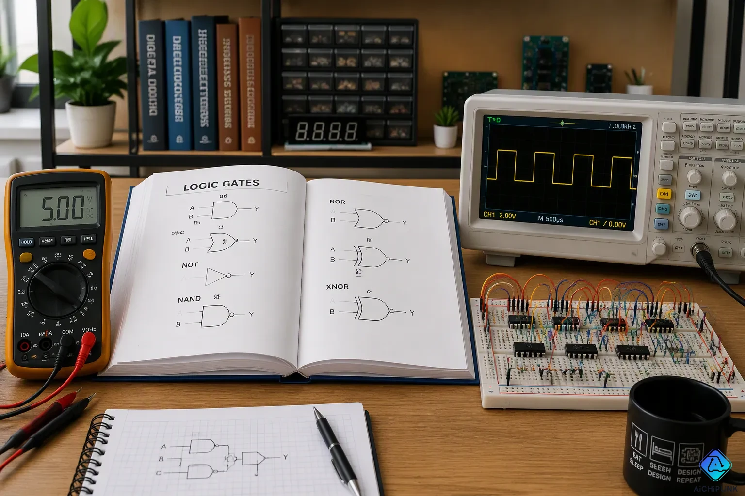
You are building a digital project, but which logic chip should you pick? A gate is the basic decision-making part in digital circuits. Common types include AND, OR, and NOT. Manufacturers group these gates into a logic family. This family gives a consistent way to build logic gate circuits. These circuits contain many different logic gates. This article compares TTL and CMOS. The first uses bipolar transistors. The second uses field-effect transistors. Each logic family has its own strengths. The first offers strong performance. The second is energy efficient. Knowing these differences helps you pick the right gate for your design.
Key Takeaways
-
TTL uses bipolar transistors and can drive strong signals, but it always uses power.
-
CMOS uses field-effect transistors and uses very little power when it is not working, so it is great for battery-powered devices.
-
Modern CMOS is faster than TTL, with signal delays as short as 2-4 ns.
-
CMOS gives better noise immunity because it has wider voltage margins.
-
Use TTL for tough factory jobs; pick CMOS for saving power and new-style designs.
Logic Gates: The Fundamentals
Basic Gates and Their Truth Tables
You start with the basic logic gates. These devices perform simple operations. The AND gate outputs a high signal only when all inputs are high. The OR gate outputs a high signal when at least one input is high. The NOT gate, also called an inverter, flips the input signal. The NAND gate is the opposite of AND. The NOR gate is the opposite of OR. You can use an AND gate, an OR gate, and a NOT gate in many projects.
Standard part numbers help you find these functions in real chips. The table below shows common TTL part numbers for AND, OR, and NOT functions.
| Logic Function | TTL Part Number |
|---|---|
| AND | 74LS08 |
| OR | 74LS32 |
| NOT | 74LS04 |
You find these devices in many everyday applications. For example:
-
Digital clock circuits: they generate pulses to measure time.
-
Digital memory circuits: they store and retrieve binary information.
-
Digital communication systems: they process signals for data transmission.
Individual chips can be cascaded together to form combinational, sequential circuits, or to produce different functions from standard chips, enabling the construction of complex digital systems from simple building blocks.
From Transistors to Integrated Circuits
Each circuit consists of transistors. For a CMOS NAND gate, the circuit uses four transistors: two PMOS in parallel and two NMOS in series. This gives a low power consumption. The bipolar design uses a different topology. The exact transistor count for a NAND gate in the other family is not specified here, but it differs from the design of the first family.
The NOR gate also has an equivalent in the other family. A quad 2-input NOR gate is available. You can use a NOR gate as a universal chip. The NOT gate is fundamental. You can use a NAND gate or a NOR gate as a universal gate. These two families are different logic families. Each logic family has its own strengths. These logic gates are the building blocks of digital circuits. Complex logic gate circuits combine multiple chips. Other logic gate circuits serve different purposes. You can combine AND and OR gates. You can use one technology or the other. The AND and OR functions are basic. This is not the only option.
TTL Logic Gate Circuits: An Overview
How TTL Works
TTL stands for Transistor-Transistor Logic. This logic family uses bipolar junction transistors (BJTs) as its core switching elements. You find these transistors arranged in a specific pattern inside each gate. The name "transistor-transistor" comes from the fact that transistors handle both the input and the output functions.
The output stage of a TTL gate uses a special configuration called a totem-pole. This design features a pair of transistors, Q3 and Q4, along with a diode D1. A resistor R4 limits the current flowing from the power supply. Under steady-state conditions, only one transistor turns on at a time. The diode D1 increases the effective turn-on voltage of Q4. This ensures Q4 turns off before Q3 fully turns on, preventing surge currents. This totem-pole arrangement lets the output actively source or sink current. You can drive capacitive loads effectively with this design.
Switching speed in TTL depends on the BJT behavior. BJTs suffer from charge storage effects in the base region. This storage slows down the switching process. Many TTL variants use Schottky diodes to address this issue. These diodes prevent deep saturation of the transistors, reducing storage time. The result is faster switching without compromising the logic function.
| Technology | Switching Speed Characteristic |
|---|---|
| MOSFET | Generally faster; can switch on and off more rapidly, ideal for high-frequency operations |
| BJT | Generally slower due to charge storage effects in the base region |
Strengths and Weaknesses of TTL
The characteristics of TTL make it a robust choice for many applications. One key strength is its high drive capability. A standard TTL gate can drive up to 10 other devices. With a buffer, you can extend this to 25–30 devices. This fan-out capacity exceeds what you need for most simple circuits.
Noise immunity is another strong point. The noise margin for standard TTL gates measures approximately 0.4 volts. This value defines the permissible voltage range for an input signal that will not alter the output logic level. TTL's solid noise margin contributes to stable and reliable logic signal levels. This robustness against electrical interference makes TTL suitable for industrial controls and legacy systems.
| Parameter | Voltage (V) | Description |
|---|---|---|
| VOH (min output HIGH) | 2.7 | Minimum voltage a TTL device will output for a HIGH signal |
| VIH (min input HIGH) | 2.0 | Minimum voltage required at an input to be recognized as HIGH |
| VOL (max output LOW) | 0.4 | Maximum voltage a TTL device will output for a LOW signal |
| VIL (max input LOW) | 0.8 | Maximum voltage allowed at an input to still be recognized as LOW |
The main weakness of TTL appears in power consumption. A standard TTL gate draws about 10 mW per gate. This figure stays constant regardless of switching state. The chart below shows this comparison clearly.
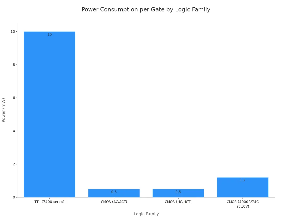
| Logic Family | Typical Power per Gate (mW) |
|---|---|
| TTL (7400 series) | 10 |
| CMOS (AC/ACT) | 0.5 |
| CMOS (HC/HCT) | 0.5 |
| CMOS (4000B/74C at 10V) | 1.2 |
This high static power consumption creates heat. Dense designs with many gates operating simultaneously generate significant heat output. You then need additional cooling mechanisms like heatsinks or fans. These add cost and complexity to your PCB layout.
CMOS gates consume almost no static power (only leakage current) when inputs are steady, whereas their power draw increases with switching frequency due to charging output capacitance. In contrast, TTL gates have a constant power draw regardless of switching state, which is why the typical 10 mW figure for TTL is a fixed baseline, while CMOS power scales with activity.
The characteristics of TTL also include defined voltage thresholds. The 0.7V gap between VOH and VIH provides noise margin. Any voltage between 0.8V and 2.0V remains undefined. This undefined zone produces an invalid state if your signal lands there.
For your design, consider TTL when you need rugged performance. Industrial controls, legacy systems, and simple circuits benefit from TTL's drive strength. The logic family excels where power efficiency matters less than reliability. You trade energy efficiency for robustness and simplicity.
CMOS Logic Gate Circuits: An Overview
How CMOS Works
CMOS stands for Complementary Metal-Oxide-Semiconductor. This logic family uses pairs of transistors that work together. Each CMOS logic gate circuit contains a p-type MOSFET and an n-type MOSFET. The p-type connects between the power supply and the output. The n-type connects between the output and ground. Both transistors share the same input signal at their gates.
This paired setup creates a push-pull action. When one transistor turns on, the other turns off. For a CMOS inverter, a high input turns on the n-type and turns off the p-type. The output then goes low. A low input does the opposite. The output goes high. This design stops any direct path from power to ground during steady states. The CMOS inverter reaches full rail-to-rail output swings. The output voltage hits the complete supply level or ground without middle steps.
The static voltage transfer curve of a CMOS inverter shows a sharp, step-like change. The output flips from high to low at a threshold voltage. This curve stays balanced around the midpoint voltage. The transition area has clear slopes. This boosts switching accuracy and lets you figure out noise tolerance easily.
Strengths and Weaknesses of CMOS
The best feature of CMOS technology is its power use. Once all circuit nodes settle with valid logic levels, no current flows. MOSFETs draw no steady-state gate current. Static power use equals the product of leakage current and supply voltage. In a CMOS logic gate circuit, one transistor always stays off. Only reverse-bias leakage currents from parasitic diodes add up. This makes idle power use very low.
This efficiency makes CMOS perfect for battery-powered devices. Older technologies drain batteries in hours. CMOS devices use power only during switching. This extends battery life during standby periods. Smartphones and portable electronics rely on this logic family for all-day use.
The traits of CMOS include a wide voltage range. CMOS can operate over a wide range of supply voltages. TTL needs a fixed 5V supply. CMOS also gives high noise immunity. The output swings rail-to-rail, offering you maximum signal margins.
However, CMOS has downsides. The high input resistance and tiny gate-source capacitance make these gates prone to electrostatic discharge. Even a small static charge creates a large voltage across the thin gate oxide. This causes breakdown. ESD is a common cause of field failures in the semiconductor industry. You must ground yourself and your equipment when handling CMOS chips.
The traits of CMOS also include faster propagation delay compared to TTL. This logic family provides both energy efficiency and high speed. For most modern uses, this trade-off works well. The 4000B series and 74C series represent common CMOS logic gate circuits. You can build NAND gates, NOR gates, and other logic functions using this logic family. The flexibility and low power draw make CMOS the top choice for new designs.
TTL vs. CMOS: Key Differences
Power, Speed, and Noise Immunity
When you compare TTL and CMOS, you see clear differences in power, speed, and noise immunity. The table below shows these key details.
| Parameter | TTL | CMOS |
|---|---|---|
| Supply Voltage | Fixed 5V | Wide range (depends on family) |
| Power Dissipation | ~10 mW per gate | Near-zero static |
| Propagation Delay | Moderate (e.g., 74xx series) | Fast (e.g., 74HC series) |
| Noise Margin | ~0.4 V | Better margins |
| Fan-Out | Typically 10 | Needs buffering |
Power use shows the biggest difference between the two families. TTL always draws a steady current, no matter if it is switching or not. So each device uses about 10 mW all the time. CMOS only uses current when it changes state. When it is not switching, it uses almost no power. This makes CMOS the clear winner for battery-powered devices. But CMOS uses more power as it switches faster. At very high speeds, the power gap between the two gets much smaller.
Speed has changed over time. Early CMOS was slower than TTL. Now, modern CMOS families are faster than TTL. Standard TTL has a moderate delay, while newer CMOS families like 74HC offer competitive speeds, and advanced families like 74AC and 74LVC are even faster. For processor cores, switching times are in picoseconds.
Noise immunity is different for the two families. TTL has fixed voltage levels. A logic low is from 0V to 0.8V. A logic high is from 2V to 5V. The noise margin is about 0.4V. CMOS thresholds change with the supply voltage, providing larger noise margins at higher voltages. This gives CMOS better protection against electrical noise. You can use CMOS reliably in noisy places. The wider margins lower the chance of false signals.
Fan-out also differs. TTL can drive up to 10 inputs. This is enough for most simple circuits. CMOS has very high input resistance. One gate barely loads the driver. But CMOS outputs cannot drive much current. You may need buffers for heavy loads. NAND and NOR gates are common building blocks. You can use a NAND gate as a universal gate. A NOR gate also works as a universal gate. The inverter is a basic building block. You use these to build complex logic circuits. These logic gates form the base of digital circuit design.
Choosing Between TTL and CMOS
Your choice depends on what you need. Think about power, speed, voltage compatibility, and drive ability. You must check each factor for your specific project. The right mix of these factors gives the best fit.
Pick TTL for high-drive, tough tasks. Industrial controls and old systems benefit from this family. It offers proven reliability. You can drive many inputs without extra parts. The fixed 5V supply makes design simple. This family works well for simple circuits with good noise margins.
Pick CMOS for energy savings, growth, and modern designs. Battery-powered devices need CMOS for long battery life. The 74HC and 74AC families give high speed with low power use. You can run them over a wide range of supply voltages. This flexibility helps when you have different power supplies. Modern logic circuits almost always use CMOS.
Critical interfacing note: TTL's logic-high output (2.7V min) may not meet CMOS's input-high requirement (which is typically higher). Use 74HCT devices or pull-up resistors. When driving TTL inputs from CMOS outputs, check current ability and timing. In mixed-voltage systems, use dedicated level translators for reliable communication.
The TTL vs CMOS choice depends on your project needs. You must pick TTL or CMOS based on your requirements. Do not assume they work together without checking datasheets. Use level translators for mixed-signal systems. You can build any function using a NAND gate. NAND is universal. You can also use a NOR gate. Each design needs careful analysis of power, speed, and noise immunity. Review your power budget, speed needs, or noise limits before choosing. Always check the specs for your specific use. The right choice ensures reliable operation.
You now understand TTL and CMOS. TTL and CMOS excel. Each logic family excels. TTL delivers robust performance for industrial applications. CMOS offers energy-efficient operation for modern designs. Do not overlook the power requirements. Prioritize low power? Pick that option. Need maximum drive strength? Pick the robust option. This logic family comparison helps you decide. You now have foundational knowledge. Experiment with both families. Consult datasheets for precise specifications. A NAND gate or a NOR gate can serve as universal gates. The inverter, NAND are basic elements. Consider your circuit needs carefully.

Written by Jack Elliott from AIChipLink.
AIChipLink, one of the fastest-growing global independent electronic components distributors in the world, offers millions of products from thousands of manufacturers, and many of our in-stock parts is available to ship same day.
We mainly source and distribute integrated circuit (IC) products of brands such as Broadcom, Microchip, Texas Instruments, Infineon, NXP, Analog Devices, Qualcomm, Intel, etc., which are widely used in communication & network, telecom, industrial control, new energy and automotive electronics.
Empowered by AI, Linked to the Future. Get started on AIChipLink and submit your RFQ online today!
Frequently Asked Questions
Can I mix TTL and CMOS chips in one project?
You can mix them, but you need care. TTL outputs may not reach the voltage CMOS expects for a high signal. Use level translators or choose 74HCT series chips. These devices bridge both families safely.
Which logic family works best for battery-powered devices?
CMOS wins for battery power. It draws almost no current when idle. TTL consumes about 10 mW per gate constantly. For portable gear, CMOS extends battery life significantly. Choose CMOS for any low-power application.
What does "fan-out" mean for my circuit design?
Fan-out tells you how many inputs one output can drive. TTL typically drives 10 inputs. CMOS has high input resistance, so one gate barely loads the driver. However, CMOS outputs handle less current. Add buffers for heavy loads.
Why are NAND and NOR gates called universal?
A NAND gate alone can build any logic function. A NOR gate also works this way. You can create AND, OR, or NOT functions using only NAND or only NOR chips. This flexibility simplifies your parts list.