Introduction
If you had to reduce all of digital electronics to a single component, many engineers would point to the NAND gate. It is the building block on which virtually everything in modern computing is constructed — from the flip-flops that store bits in CPU registers, to the address decoders in memory chips, to the billions of logic cells packed into modern FPGAs and ASICs. The reason for this central role is a remarkable property: every possible logic function can be implemented using nothing but NAND gates. This makes the NAND gate what engineers call a universal gate.
Yet for students and newcomers to digital electronics, the NAND gate is often where confusion begins. What does "NAND" actually mean? How do you read its truth table? Why does putting two NAND gates together create a NOT gate? And how does a real NAND gate — made of transistors on a silicon chip — actually perform this logic operation?
This guide answers every one of those questions. Whether you are studying for an exam, designing a circuit, or simply trying to understand how computers work from the ground up, this is the most complete reference on NAND gates available in one place.
1.0 What Is a NAND Gate? Definition and Core Concept
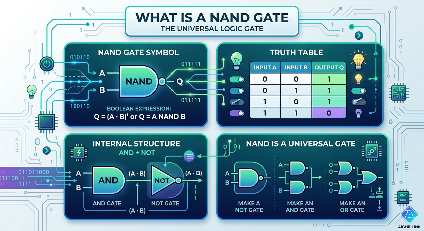
A NAND gate is a digital logic gate that produces a LOW (0) output only when ALL of its inputs are HIGH (1). For any other combination of inputs — including all inputs LOW, or a mix of HIGH and LOW — the output is HIGH (1).
The name NAND is a contraction of NOT AND. To understand this, start with the AND gate: an AND gate produces a HIGH output only when all inputs are HIGH. The NAND gate is simply an AND gate followed by a NOT (inverter) stage — it takes the AND result and flips it. Where AND gives 1 only when all inputs are 1, NAND gives 0 only when all inputs are 1.
This single rule — output is LOW only when all inputs are HIGH — governs every NAND gate in existence, regardless of how many inputs it has, what technology it is made from, or what voltage levels represent logic HIGH and LOW in the system.
A useful intuition: think of a NAND gate as a "NOT all HIGH" detector. Its output says: "Are all my inputs HIGH? If yes — and only then — my output goes LOW." In every other situation, the output stays HIGH.
1.1 NAND Gate Logic Symbol (IEEE, ANSI, and IEC)
Two symbol standards are used in circuit diagrams worldwide:
IEEE/ANSI symbol (most common in the USA): The NAND gate uses the same curved "D-shaped" body as the AND gate, with a small circle (bubble) added at the output. The bubble universally represents inversion (NOT) in logic diagrams — its presence on the AND body shape immediately communicates "AND, then inverted."
IEC 60617 / DIN symbol (common in Europe): Uses a flat rectangle with an "&" symbol inside (indicating the AND function) and a bubble at the output. All inputs enter from the left; the output exits from the right with the inversion bubble.
In both systems, the bubble at the output is the defining feature of the NAND symbol — it distinguishes the NAND from the plain AND gate at a glance.
For a 2-input NAND gate: inputs are labeled A and B (or In1 and In2), and the output is labeled Y (or Q, or F depending on the schematic convention).
1.2 NAND Gate Boolean Expression
The Boolean algebra expression for a 2-input NAND gate is:
Y = A · B (overline over entire expression) = NOT (A AND B)
In standard notation this is written with a bar over the entire AND expression:
Y = ̄(A · B)
which is read as "Y equals NOT of (A AND B)" or "Y equals A NAND B."
Some textbooks use the alternative notation:
Y = A ↑ B
where the ↑ symbol (Sheffer stroke) specifically denotes the NAND operation — named after logician Henry M. Sheffer, who proved in 1913 that the NAND operation alone is sufficient to express all Boolean functions.
For a 3-input NAND gate, the expression extends naturally:
Y = ̄(A · B · C) = NOT (A AND B AND C)
The output is LOW only when A = 1, B = 1, AND C = 1 simultaneously. Any other combination produces Y = 1.
1.3 De Morgan's Theorem and the NAND Gate
De Morgan's Theorem provides an alternative but equivalent way to express the NAND function that reveals its deep relationship to the OR gate:
̄(A · B) = Ā + B̄
In words: "NOT of (A AND B)" equals "(NOT A) OR (NOT B)"
This equivalence has a profound practical consequence: a NAND gate is identical in behavior to an OR gate with inverted inputs. If you take an OR gate and add inversion bubbles on both inputs (instead of on the output), you get functionally the same circuit as a NAND gate.
This is why logic diagrams sometimes show a NAND gate drawn as an OR gate with bubbles on both inputs — it is an alternative representation called the De Morgan equivalent symbol. Both symbols represent exactly the same physical gate and produce exactly the same output for every input combination.
The De Morgan equivalence also has a direct design application: when two bubbles meet at a connection point in a logic diagram (one bubble on an output driving another bubble on an input), they cancel out — a powerful simplification technique for minimizing inversion stages in complex logic circuits.
2.0 NAND Gate Truth Table
2.1 2-Input NAND Gate Truth Table
The truth table is the definitive, complete specification of a logic gate — it lists every possible input combination and the corresponding output. For a 2-input NAND gate:
| Input A | Input B | AND Result (A·B) | NAND Output Y = ̄(A·B) |
|---|---|---|---|
| 0 | 0 | 0 | 1 |
| 0 | 1 | 0 | 1 |
| 1 | 0 | 0 | 1 |
| 1 | 1 | 1 | 0 |
Reading the table: Only in the last row — where both A AND B are 1 — does the AND result become 1, which the NOT stage then inverts to 0. In all other three rows, the AND result is 0, which inverts to 1. The NAND gate output is therefore 1 in three out of four possible input combinations.
Memory shortcut: A 2-input NAND gate outputs 0 for exactly one input combination (1,1) and outputs 1 for all others. Conversely, a 2-input AND gate outputs 1 for exactly one combination (1,1). The NAND is the AND's mirror image.
2.2 3-Input NAND Gate Truth Table
A 3-input NAND gate has 2³ = 8 possible input combinations:
| A | B | C | A·B·C | Y = ̄(A·B·C) |
|---|---|---|---|---|
| 0 | 0 | 0 | 0 | 1 |
| 0 | 0 | 1 | 0 | 1 |
| 0 | 1 | 0 | 0 | 1 |
| 0 | 1 | 1 | 0 | 1 |
| 1 | 0 | 0 | 0 | 1 |
| 1 | 0 | 1 | 0 | 1 |
| 1 | 1 | 0 | 0 | 1 |
| 1 | 1 | 1 | 1 | 0 |
Again, there is exactly one row where the output is 0 — when all three inputs are simultaneously 1. For all seven other combinations, Y = 1. This pattern holds for any number of inputs: an N-input NAND gate has output 0 for exactly one of its 2ᴺ input combinations.
2.3 NAND vs. AND vs. NOR Gate: Side-by-Side Comparison
| A | B | AND (A·B) | NAND ̄(A·B) | OR (A+B) | NOR ̄(A+B) | XOR (A⊕B) |
|---|---|---|---|---|---|---|
| 0 | 0 | 0 | 1 | 0 | 1 | 0 |
| 0 | 1 | 0 | 1 | 1 | 0 | 1 |
| 1 | 0 | 0 | 1 | 1 | 0 | 1 |
| 1 | 1 | 1 | 0 | 1 | 0 | 0 |
Key observations from this table:
- NAND is the inverse of AND — their output columns are exact complements of each other
- NOR is the inverse of OR — their output columns are exact complements
- NAND outputs 0 only once (when both inputs are 1); NOR outputs 0 three times out of four
- NAND and NOR are both universal gates — the entire logic family can be built from either one alone
3.0 NAND as a Universal Gate
The most important property of the NAND gate in practical digital design is its universality: every logic function that can be expressed in Boolean algebra can be implemented using only NAND gates. No other gate type is needed. This is why semiconductor manufacturers can implement any digital logic design — from simple combinational circuits to full CPUs — using a single type of logic cell.
The practical consequence in chip design is significant: standardizing on one gate type simplifies the design, layout, and verification of standard cell libraries in ASIC and FPGA design flows. NAND-based synthesis is the default in most digital synthesis tools.
3.1 Building a NOT Gate from NAND
The simplest NAND-only construction is the NOT (inverter) gate. Connect both inputs of a 2-input NAND gate together:
Y = ̄(A · A) = ̄A
Because A AND A is simply A (a number ANDed with itself is itself), the NAND gate with tied inputs reduces to NOT A. Connect both input terminals to the same signal, and the output is the inverted signal.
Truth table verification:
| A (both inputs tied) | Y = ̄(A·A) |
|---|---|
| 0 | 1 |
| 1 | 0 |
This is exactly a NOT gate. One NAND gate, inputs tied together = one inverter. This is the most resource-efficient construction possible.
3.2 Building an AND Gate from NAND
An AND gate requires two NAND gates: the first NAND gate performs the NAND operation, and the second NAND gate (with its inputs tied together) acts as an inverter to undo the inversion:
First NAND: W = ̄(A·B) Second NAND (inverter): Y = ̄(W·W) = ̄W = ̄(̄(A·B)) = A·B
The double negation cancels, recovering the AND function. This requires one 2-input NAND + one inverter NAND = 2 NAND gates total.
Note that this is less efficient than a native AND gate — the extra inverter stage adds propagation delay. In delay-critical paths, native AND gates are preferred when available. In NAND-only implementations, this two-gate AND is the standard construction.
3.3 Building an OR Gate from NAND
Applying De Morgan's theorem (̄(A·B) = Ā + B̄) in reverse: an OR gate can be built by inverting both inputs before the NAND operation:
Y = ̄(Ā · B̄) = A + B
This requires two inverter NANDs (one for each input) plus one 2-input NAND for the operation itself = 3 NAND gates total.
Alternatively, using three 2-input NAND gates with tied inputs for the first two stages and a NAND for the third stage achieves OR in exactly 3 gates.
3.4 Building an SR Latch from NAND Gates
One of the most important NAND-only circuits is the SR (Set-Reset) latch — the simplest form of bistable memory, capable of storing a single bit. It requires exactly two NAND gates, with each gate's output feeding back to one input of the other gate:
Circuit connections:
- NAND Gate 1: inputs are S (Set) and Q_bar (output of Gate 2); output is Q
- NAND Gate 2: inputs are R (Reset) and Q (output of Gate 1); output is Q_bar
SR Latch truth table (NAND-based — note: inputs are active-LOW):
| S | R | Q (output) | Q_bar | State |
|---|---|---|---|---|
| 1 | 1 | Last Q | Last Q_bar | Memory — holds previous state |
| 0 | 1 | 1 | 0 | Set — Q goes HIGH |
| 1 | 0 | 0 | 1 | Reset — Q goes LOW |
| 0 | 0 | 1 | 1 | Forbidden — both outputs HIGH, undefined behavior |
The NAND SR latch has active-LOW inputs: asserting S (pulling it LOW) sets the latch; asserting R (pulling it LOW) resets it. When both inputs are HIGH (inactive), the latch holds its previous state — it remembers. This feedback-based memory is the foundation of all flip-flops, registers, and SRAM cells in digital electronics.
The SR latch demonstrates why NAND gates are so fundamental: two simple gates, connected with feedback, create a memory element — something qualitatively different from either gate alone.
4.0 CMOS Implementation, IC Packages & Applications
4.1 How a NAND Gate Is Built in CMOS
The most widely used NAND gate implementation is CMOS (Complementary Metal-Oxide-Semiconductor) — the transistor technology used in virtually every modern digital IC. A 2-input CMOS NAND gate uses four transistors: two PMOS (P-channel) and two NMOS (N-channel).
Circuit structure:
-
Pull-up network (PMOS, connected to VDD): Two PMOS transistors connected in parallel. PMOS transistors turn ON when their gate is LOW (0). If either A OR B is LOW, the corresponding PMOS transistor conducts, connecting the output to VDD (HIGH).
-
Pull-down network (NMOS, connected to GND): Two NMOS transistors connected in series. NMOS transistors turn ON when their gate is HIGH (1). Only when BOTH A AND B are HIGH do both NMOS transistors conduct simultaneously, connecting the output to GND (LOW).
Why this circuit implements NAND logic:
- If A = 0 OR B = 0 (or both): at least one PMOS is ON → output is pulled to VDD = HIGH (1). The NMOS chain is broken (at least one NMOS is OFF), so there is no path to GND.
- If A = 1 AND B = 1: both PMOS are OFF (no path to VDD); both NMOS are ON (complete path to GND) → output is pulled to GND = LOW (0).
This is exactly the NAND truth table. The parallel PMOS / series NMOS structure naturally implements the NAND function — a fundamental insight of CMOS logic design.
Transistor count efficiency: The CMOS NAND gate uses 4 transistors for 2 inputs. A CMOS AND gate requires 6 transistors (NAND stage + inverter stage). This is why NAND is the preferred primitive in CMOS logic synthesis — it is intrinsically more area-efficient than AND.
4.2 Propagation Delay, Noise Margin, and Fan-Out
Propagation delay (tpd): The time from when an input changes to when the output reaches its new stable value. For the 74HC00 quad 2-input NAND gate in HCMOS technology, typical tpd is 7 ns at 5V. For 74LS00 (bipolar TTL), typical tpd is 9 ns. Propagation delay matters in high-speed designs — cascading multiple NAND stages multiplies the delay, and long chains of gates set a lower limit on the maximum clock frequency of a synchronous system.
Noise margin: The voltage margin between the guaranteed output level of a driving gate and the worst-case input threshold of a driven gate. For 74HC-series CMOS at 5V: VOH(min) = 4.4V, VIH(min) = 3.5V → HIGH noise margin = 0.9V. VOL(max) = 0.1V, VIL(max) = 1.0V → LOW noise margin = 0.9V. Wider noise margins mean greater immunity to noise on signal lines — a key advantage of CMOS over older bipolar TTL logic.
Fan-out: The number of gate inputs that one gate output can reliably drive. For 74HC-series CMOS, fan-out is 10 (can drive 10 74HC inputs) at DC. At high switching speeds, capacitive loading reduces the effective fan-out — each additional input adds capacitance that slows the output's rise and fall times, increasing propagation delay. For critical high-speed paths, limit fan-out to 4–6 loads and use buffers for high-fanout nets.
4.3 Common NAND Gate ICs: 74HC00, 74LS00, CD4011
The most widely available NAND gate ICs are quad 2-input packages — four independent 2-input NAND gates in a single 14-pin DIP or SOIC package:
| Part Number | Logic Family | VCC Range | tpd (typical) | IOL Max | Package |
|---|---|---|---|---|---|
| 74HC00 | HCMOS | 2V – 6V | 7 ns @ 5V | 4 mA | 14-pin DIP / SOIC |
| 74HCT00 | HCMOS (TTL-compatible input) | 4.5V – 5.5V | 9 ns | 4 mA | 14-pin DIP / SOIC |
| 74LS00 | Low-Power Schottky TTL | 4.75V – 5.25V | 9 ns | 8 mA | 14-pin DIP / SOIC |
| 74AHC00 | Advanced HCMOS | 2V – 5.5V | 3.8 ns | 8 mA | 14-pin SOIC / TSSOP |
| CD4011B | CMOS (4000-series) | 3V – 18V | 35 ns @ 10V | 0.4 mA | 14-pin DIP / SOIC |
| SN74LVC00A | LVC (Low-Voltage CMOS) | 1.65V – 3.6V | 3.8 ns | 24 mA | 14-pin SOIC / TSSOP |
Choosing between families:
- 74HC00 — the default choice for 5V CMOS systems; good speed, low power, widely available
- 74HCT00 — use when interfacing with 5V TTL-level outputs (inputs are TTL-compatible)
- 74LS00 — legacy TTL for older designs or when driving TTL loads directly
- CD4011B — choose when wide supply voltage range (3–18V) is needed; slower speed
- 74LVC00A — for 3.3V and lower-voltage systems (1.65–3.6V)
Pin numbering for all quad 2-input NAND packages (74x00 series) follows the same standard: pins 1–2 are inputs to gate 1, pin 3 is the output; pins 4–5 are inputs to gate 2, pin 6 is the output; and so on. Pin 7 is GND, pin 14 is VCC.
4.4 Where NAND Gates Are Used in Real Electronics
NAND gates appear in virtually every digital system ever built. Some of the most important applications:
NAND Flash Memory: The storage technology in every USB drive, SSD, smartphone, and memory card is named after the NAND gate — its memory cells are organized in series strings analogous to the series NMOS configuration in a NAND gate circuit. NAND flash offers higher density and lower cost per bit than NOR flash, making it the dominant non-volatile memory technology in consumer electronics.
CPU and microcontroller logic: Every arithmetic, logic, and control operation inside a CPU is ultimately implemented as a network of NAND (and NOR) gates. Modern processors contain billions of NAND-derived logic cells implementing adders, multiplexers, decoders, and registers.
SRAM bit cells: Static RAM uses a 6-transistor cell built from two cross-coupled CMOS inverters (which are NAND-related circuits) plus access transistors. Every cache level in a CPU is a dense array of these cells.
Debounce circuits: A NAND SR latch (as described in Section 3.4) is the standard circuit for debouncing mechanical switch contacts — preventing the multiple false triggers that result from mechanical bounce when a button is pressed.
Combinational logic in control systems: Address decoders in microprocessor memory maps, priority encoders, multiplexers, and comparators are all routinely implemented using NAND gate networks in standard cell ASIC designs.
5.0 Where to Buy NAND Gate ICs
NAND gate ICs are among the most widely stocked and lowest-cost logic components in the industry. For prototyping and production, the 74HC00 is available at essentially every electronics distributor worldwide — DigiKey, Mouser, Arrow, Avnet, and LCSC all carry extensive stock of 74HC00 and related NAND gate ICs from manufacturers including Texas Instruments, Nexperia, ON Semiconductor, and STMicroelectronics.
For sourcing NAND gate ICs and other digital logic components with verified authenticity, competitive pricing, and volume procurement support, visit aichiplink.com.
6.0 Conclusion
The NAND gate is one of the most important components in all of digital electronics — not despite its simplicity, but because of it. A single rule (output is LOW only when all inputs are HIGH) gives rise to a component that can construct every other logic function, store bits in memory, synchronize circuits, and ultimately form the entire computational fabric of modern digital systems.
Understanding the NAND gate means understanding: its Boolean expression (Y = NOT(A AND B)), its truth table (output is 1 for all combinations except all-inputs-1), its De Morgan equivalence (identical to OR with inverted inputs), its universality (NOT, AND, OR, XOR, SR latch — all built from NAND alone), its CMOS implementation (4 transistors: parallel PMOS for pull-up, series NMOS for pull-down), and its real-world presence (from the 74HC00 on your breadboard to the NAND flash in your smartphone).
With these concepts firmly in hand, the rest of digital logic design — combinational circuits, sequential circuits, state machines, and beyond — builds naturally on this foundation.
For sourcing 74HC00, 74LS00, CD4011, and all other NAND gate IC families, explore verified inventory with competitive pricing at aichiplink.com.

Written by Jack Elliott from AIChipLink.
AIChipLink, one of the fastest-growing global independent electronic components distributors in the world, offers millions of products from thousands of manufacturers, and many of our in-stock parts is available to ship same day.
We mainly source and distribute integrated circuit (IC) products of brands such as Broadcom, Microchip, Texas Instruments, Infineon, NXP, Analog Devices, Qualcomm, Intel, etc., which are widely used in communication & network, telecom, industrial control, new energy and automotive electronics.
Empowered by AI, Linked to the Future. Get started on AIChipLink.com and submit your RFQ online today!
Frequently Asked Questions
Why is the NAND gate called a "universal gate"?
A NAND gate is called a universal gate because any digital logic function can be built using only NAND gates. This means circuits like NOT, AND, OR, XOR, and even complex systems such as adders and flip-flops can be implemented without using any other gate type, making NAND extremely versatile in digital design.
What is the difference between a NAND gate and an AND gate?
The key difference is that a NAND gate is the inverse of an AND gate. An AND gate outputs 1 only when all inputs are 1, while a NAND gate outputs 0 in that case and 1 otherwise. In CMOS design, NAND gates are more efficient because they require fewer transistors, which is why they are preferred in most digital circuits.
Can a NAND gate have more than two inputs?
Yes, NAND gates can have multiple inputs such as 2, 3, 4, or more. The logic remains the same—output is 0 only when all inputs are 1—but as the number of inputs increases, performance may decrease due to higher internal resistance, so designers often use smaller NAND gates in combination.
What happens if one input of a NAND gate is tied to HIGH?
If one input of a NAND gate is permanently tied to logic HIGH, the gate functions as a NOT (inverter) for the other input. This technique is commonly used in circuit design to reuse unused NAND gates and ensure stable input conditions.
What is the difference between a NAND gate and a NOR gate?
A NAND gate outputs 0 only when all inputs are 1, while a NOR gate outputs 1 only when all inputs are 0. Both are universal gates, but NAND is more widely used in CMOS circuits because it offers better speed and efficiency due to its transistor configuration.