Why the TTL NAND gate output goes low only when every input is high
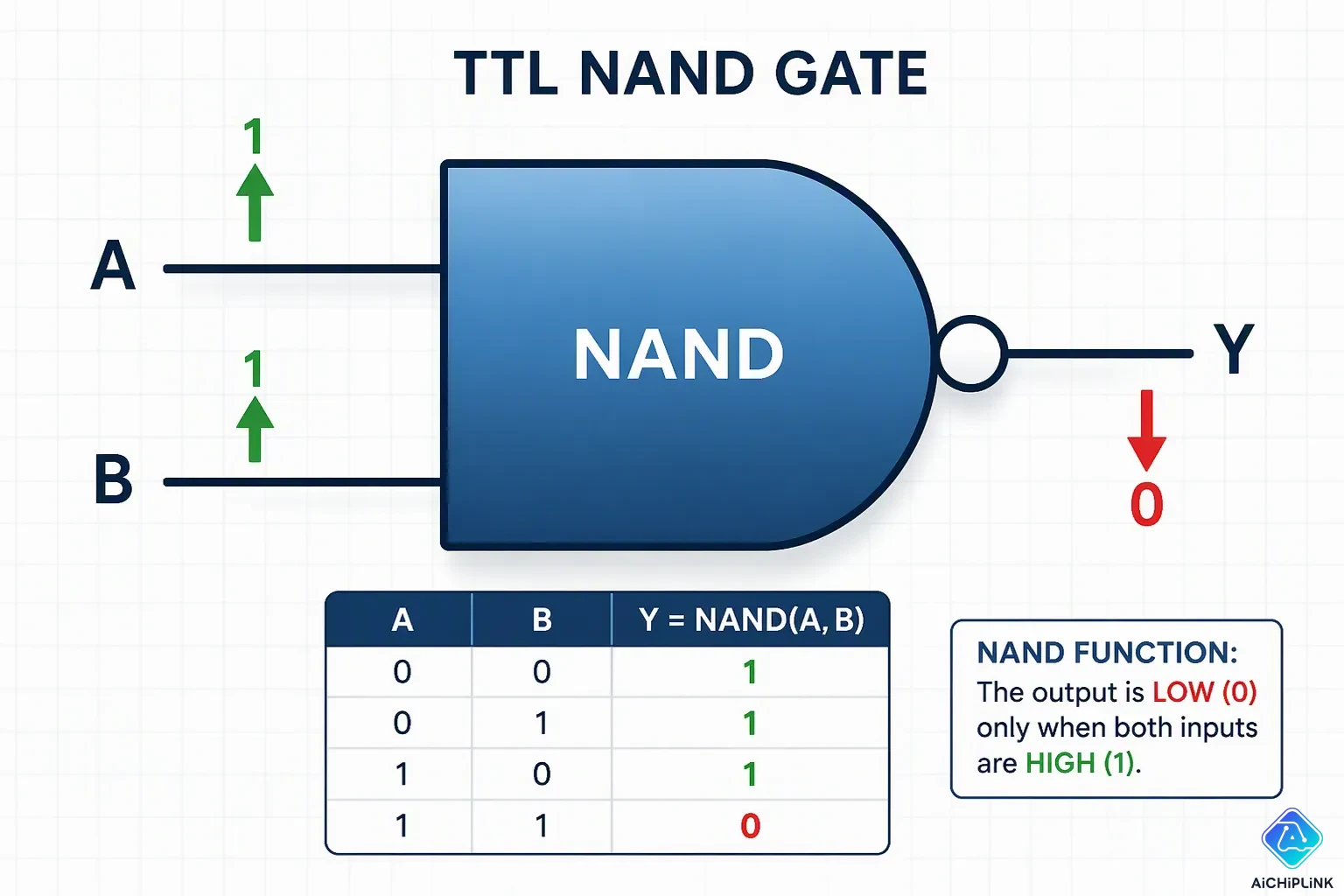
A TTL NAND gate output goes low only when every input is high because the internal transistors create a conduction path to ground solely under that condition. You see this behavior in the nand gate’s design: the multi-emitter input transistor and the output stage work together. When any input sits at a low logic level, that path stays blocked. The ttl nand gate then holds its output high. Conversely, when all inputs reach a high state, the path opens, and the output drops low. This post traces the nand’s internal transistors step by step. You will see exactly how each input level influences the final output.
Key Takeaways
-
A TTL NAND gate output goes low only when every input is high, because the internal transistors make a path to ground only in that case.
-
The multi-emitter input transistor sends current to the phase splitter only when all inputs are high; any low input pulls current away, so the output stays high.
-
The phase splitter and totem-pole output stage work as a team: when every input is high, the pull-down transistor turns fully on and brings the output low; if not, the pull-up transistor holds the output high.
-
The truth table of a NAND gate shows what the transistors do: the output is high for every input mix, except when all inputs are high, then it goes low.
-
Knowing how the transistors inside a logic gate work helps you guess its output. You can do this by following the path that electricity takes from the inputs to the output.
Inside the TTL NAND Gate
Every TTL NAND gate has three internal stages that work together to make the correct logic output. You can think of these stages as a chain. Each one passes a signal to the next.
-
The multi-emitter input transistor takes in the logic inputs.
-
The control section, built around the phase splitter, handles signal inversion.
-
The totem-pole output stage drives the final logic level.
This ttl design uses bipolar junction transistors throughout. The setup is simple, but it produces reliable switching.
The Multi-Emitter Input Transistor
The first stage is one transistor with multiple emitters. Each emitter connects to one input pin of the chip. This transistor acts as the input stage for the classic TTL NAND gate. It does the AND function at the transistor level. When all inputs are high, the input transistor enters a state that turns on the phase-splitter transistor. When any single input is pulled low, the input transistor saturates through that emitter instead. This action keeps the phase splitter off. The multi-emitter transistor thus does the AND function. The output goes low only when all inputs are high. The output stage then flips this result to make NAND logic.
The Phase Splitter and Output Stage
The phase splitter transistor, labeled Q2, drives both halves of the output stage. It makes opposite-phase input conditions. This lets the pull-up and pull-down output transistors work in antiphase. One stays on while the other stays off. Q2 flips the phase of the signal from Q1. It also gives both in-phase and out-of-phase signals to the next stage.
The output stage uses a totem-pole setup. This push-pull arrangement has an active pull-down transistor and an emitter-follower pull-up transistor. A steering diode limits at-the-same-time conduction during switching. When the pull-down transistor saturates, the output goes low. When the pull-down is cut off, the upper transistor acts as an emitter follower. It then makes a high output at low impedance. The diode and series resistor limit transient current. They also cut shoot-through current between the supply rails. One known limit of this ttl circuitry is that the logical high output voltage drops to typically 3.5 V, even with no load. This drop comes from voltage losses across the pull-up transistor's base-emitter junction and the steering diode.
How the NAND Gate Input Transistor Responds
The multi-emitter transistor Q1 acts as a current-steering element. It does not amplify signals like a normal transistor. Instead, it directs current from resistor R1 either out through an emitter or into Q2's base. This steering action depends entirely on the input logic levels you apply.
When Any Input Is Low
You ground one emitter when either of the inputs is grounded. That grounded ("low") input forward-biases the base-emitter junction for that emitter. Current from R1 and Q1's base then flows out through that emitter into the low input. This action pulls Q1's base voltage down. Q2's base becomes starved of current. As a result, Q2 and Q4 turn off.
When either or both inputs A and B are off (logic 0 or low), transistors Q2 and Q4 turn off to create a logic 1 or high logic output.
With Q4 off, R3 pulls Q3's base low. Q3 turns off. The output floats to a high state through the pull-up path. So a single low input at any emitter keeps the nand gate output is high. The transistor never sends current to Q2 under this condition.
When Every Input Is High
Now suppose all inputs reach a high logic level. No emitter provides an escape path for R1's current. The current cannot exit through any emitter. So it flows backward out of Q1's collector into Q2's base. This turns Q2 on.
If all inputs are HIGH (logic 1), all emitters are forward biased, allowing current to flow from the base to the emitters. This causes the transistor to conduct, pulling the base of the next transistor low.
Q2 then pulls Q3's base high. Q3 turns on and pulls the output low. This confirms the NAND behavior. The input transistor only steers current to Q2 when every input sits at a high logic level. Any single low input breaks that path.
How the TTL NAND Gate Output Goes Low
The output stage only pulls down when the phase splitter passes current to the pull-down transistor. That handoff happens under one condition: every input sits at a high logic level. You can trace this chain from Q1 through Q2 to Q3 and watch the output of the nand gate drop.
Q2 Saturates and Turns On Q3
When both inputs reach the logic HIGH state defined by the TTL family, with a minimum input voltage of 2 V, current flows through the base-collector junction of Q1 into the base of Q2. This current drives Q2 into saturation. A saturated transistor conducts heavily and its collector voltage drops close to its emitter voltage. That low collector voltage then feeds the base of Q3.
When both the inputs are in the logic HIGH state as specified by the TTL family (VIH = 2 V minimum), the current flows through the base-collector PN junction diode of transistor Q1 into the base of transistor Q2. Transistor Q2 is turned ON to saturation, with the result that transistor Q3 is switched OFF and transistor Q4 is switched ON.
Q2 must reach saturation for this to work. A partially on Q2 would not supply enough base current to Q3. Q3 would stay in its active region and never pull the output down hard. Saturation guarantees a strong drive signal. Once Q3 receives that drive, it turns on and connects the output node to ground.
This low state is the complement of AND logic. An AND gate produces a high output only when all inputs are high. The nand gate inverts that result. This inversion is exactly why ttl nand and and gates differ at the output pin even though they share the same input stage behavior.
The Totem-Pole Path to Ground
The totem-pole output stage uses two stacked transistors. The upper device pulls the output high. The lower device, Q4, pulls it low. When Q4 saturates, it acts as a low-impedance path to ground. The output voltage then drops below 0.4 V, which the next stage reads as a solid logic low.
The totem-pole output includes pull-down transistors that provide a low-impedance path to ground, enabling the output to be pulled LOW effectively when required.
Here is the full state of every transistor when all inputs are high:
| Condition | Q1 state | Q2 state | Q4 state | Q3 state | Output |
|---|---|---|---|---|---|
| All inputs HIGH | Reverse-active (provides base current to Q2) | ON | Saturated (acts as low-impedance path to ground) | OFF | LOW (<0.4V) |
Notice that Q3 stays off in this state. The phase splitter Q2 drives Q3 and Q4 in antiphase. When Q2 saturates, it turns Q4 on and Q3 off. The totem-pole arrangement never lets both output transistors conduct at once. That design keeps the output impedance low in both the high and low states.
The low-impedance path matters for speed. A saturated pull-down transistor sinks current quickly. The output of the nand gate transitions to a valid low level without waiting for a weak pull-down resistor. This is why TTL gates drive other TTL inputs reliably. The nand gate’s output can sink enough current to hold many fan-out loads at a valid low level.
You now see the full chain. All inputs high means Q1 steers current into Q2. Q2 saturates. Q4 saturates. The output goes low. Any single low input breaks this chain at the first transistor.
The NAND Input-Output Relationship
Mapping Transistor States to Logic Levels
You can now connect every transistor state to a logic level. The table below shows the complete truth table for a two-input NAND gate. This table comes directly from the transistor behavior you just traced.
| Input A | Input B | Output Y |
|---|---|---|
| 0 | 0 | 1 |
| 0 | 1 | 1 |
| 1 | 0 | 1 |
| 1 | 1 | 0 |
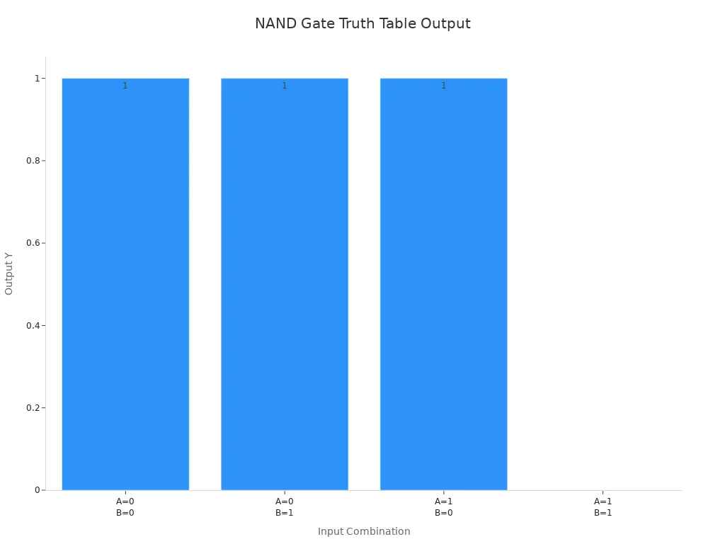
The rule for a NAND gate is simple. The output stays high unless every input is high. TTL defines a high signal as any voltage above 2V. When any input sits below that threshold, the input transistor steers current away from the phase splitter. The output then holds a high logic level. When all inputs rise above 2V, the transistor chain pulls the output low.
This behavior gives you the nand function. Notice how the output column is the exact opposite of an AND gate. The inverted-output nand gate produces a low only in the final row. Every other combination yields a high output.
Why Other Gates Behave Differently
The ttl nand and and gates share the same input stage. They differ only at the output. An and gate adds an inverter stage after the NAND output. That extra stage flips the low state back to high. So the and gate produces a high output only when all inputs are high.
Other gate types change the input transistor arrangement. An OR gate uses parallel conduction paths instead of series steering. Its output goes high when any input goes high. The internal transistor network determines which input logic levels trigger a low output.
You can apply this same method to any gate. Trace the conduction path from the inputs through the phase splitter to the output stage. The truth table then follows naturally from the transistor states. The physical behavior always matches the logic you already know.
You now know why a ttl nand gate output goes low only when every input sits at a high logic level. The transistor design creates a path to ground only under that condition. Any single low input breaks the chain before it reaches the output stage.
Connect this physical behavior back to the truth table you already know. Each row matches a real transistor state inside the nand gate. The nand function is not abstract. It comes from current steering through the input transistor and the phase splitter.
Next time you see a nand gate symbol, picture those internal transistors. The logic levels and the silicon tell the same story.

Written by Jack Elliott from AIChipLink.
AIChipLink, one of the fastest-growing global independent electronic components distributors in the world, offers millions of products from thousands of manufacturers, and many of our in-stock parts is available to ship same day.
We mainly source and distribute integrated circuit (IC) products of brands such as Broadcom, Microchip, Texas Instruments, Infineon, NXP, Analog Devices, Qualcomm, Intel, etc., which are widely used in communication & network, telecom, industrial control, new energy and automotive electronics.
Empowered by AI, Linked to the Future. Get started on AIChipLink and submit your RFQ online today!
Frequently Asked Questions
Why does the TTL NAND gate output go low only when every input is high?
The multi-emitter transistor steers current to the phase splitter only when all inputs sit at a logic 1. That current turns on the pull-down transistor. The output then connects to ground. Any logic 0 at an emitter breaks this path.
What happens inside the gate when one input is low?
A logic 0 at one input forward-biases one emitter of the input transistor. Current escapes through that emitter instead of reaching the phase splitter. The pull-down transistor stays off. The output remains at a logic 1.
How does the truth table connect to the transistor states?
Each row of the truth table matches a real transistor state. When all inputs sit at a logic 1, the nand pulls the signal low. Every other combination keeps it at a logic 1. The silicon and the logic agree.
Why does an AND gate produce a different output than a NAND gate?
Both share the same first stage. An and gate adds an inverter after the nand output. That extra stage flips the logic 0 state back to a logic 1. So it outputs a logic 1 only when all pins sit at a logic 1.
What defines a logic level in TTL?
TTL defines a logic level above 2 V as a 1. A voltage below that threshold is a 0. These input logic levels decide which path the current takes inside the gate.