How to Properly Install TVS Diodes in Your PCB Design
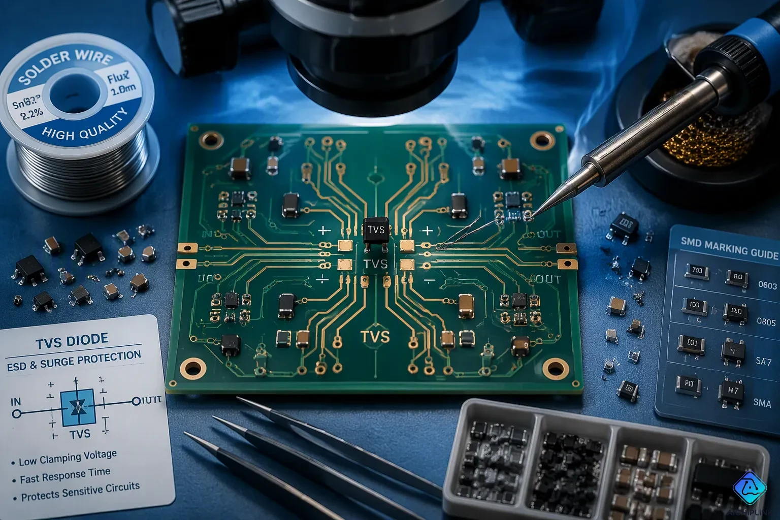
TVS diodes must sit as close as possible to the electrostatic discharge entry point—an exposed connector or I/O port. You install TVS diodes there to clamp transient voltage suppression before voltage spikes travel deeper into your circuit. The shorter your surge current path, the lower your parasitic inductance. Lower inductance prevents high voltage spikes from overshooting and damaging sensitive components downstream.
Why does your ESD protection circuit fail even with the correct TVS? Most engineers overlook installation physics. They focus on component ratings, not placement. Yet circuit protection depends heavily on physical layout. Poor soldering, excessive thermal resistance, or inadequate cooling under repetitive surges can degrade clamping performance silently. These TVS diodes require careful PCB design considerations.
Have you ever wondered why your protection circuit failed despite using the correct diode? This article provides practical layout-focused advice for your PCB—safety steps that prevent static discharge damage. Your ESD protection strategy needs proper PCB grounding and trace management to handle voltage spikes effectively.
Key Takeaways
-
Put TVS diodes 3-5 mm from the connector. This cuts inductance and stops voltage spikes.
-
Connect TVS diodes to a low-impedance chassis ground using short, wide traces and multiple vias.
-
To get proper clamping, use bidirectional TVS diodes for bipolar signals such as RS-485 or CAN bus.
-
Route the traces in a straight line from the connector to the diode, and don't use vias or series parts in between.
-
Check the polarity of unidirectional TVS diodes to prevent silent failure during transients.
Placement of TVS Diodes Near ESD Entry Points
The physical location of your TVS diodes determines whether your ESD protection circuit saves your design or fails silently. You must install TVS diodes as close as physically possible to the entry point of electrostatic discharge. That entry point usually means an exposed connector, a push-button, or an I/O port where a human finger or cable can deliver a static charge. Every millimeter of distance between the connector pin and the diode adds parasitic inductance to the surge path. That inductance creates voltage overshoot during fast transients, which defeats the purpose of your protection.
Proximity to Connectors and I/O Ports
Place the TVS diode right at the connector edge, before any series parts like resistors, inductors, or ferrite beads. Series parts slow down the transient current from reaching the clamp quickly. If you put a resistor between the connector and the diode, the voltage drop across that resistor shows up at the protected IC before the diode can clamp it. The diode must see the surge first.
For through-hole connectors, you have some options. You can mount the diode between the pins on the same side of the board, or you can put it on the back side right under the connector. Both ways work, but you must keep trace lengths very short. A useful rule from layout studies says to place TVS arrays within 3–5 mm of the connector pins. The whole ESD current loop, from connector pin through the diode to the ground via, should stay under 5 mm in total trace length.
Each extra millimeter of trace adds about 1 nH of inductance. During an IEC 61000-4-2 electrostatic discharge event, current rises very fast. That inductance can turn into several volts of unwanted overshoot. A normal 5 V clamp can rise to 12 V in practice with poor layout. Such overshoot can easily go past the maximum ratings of sensitive transceivers or microcontrollers.
Put a wide ground via within 2–3 mm of the TVS diode pad. This placement cuts down the return path inductance. Route traces straight from the discharge source to the diode without changing layers whenever you can.
Avoid vias in the transient suppression circuit: Route traces straight from the discharge source to the diode without changing layers. Via inductance can push current to the protected IC and raise voltage spikes, weakening protection.
Orientation and Polarity for Unidirectional TVS
Unidirectional TVS diodes need the right orientation for your ESD protection circuit to work. These diodes conduct in one direction only. You must connect the cathode to the positive supply rail or signal line and the anode to ground. If you flip the diode, it will not clamp during a transient and may get damaged.
| Property | Unidirectional TVS (correctly oriented) | Bidirectional TVS |
|---|---|---|
| Clamping direction | Blocks up to rated voltage in one direction only (reverse bias); acts like a forward-biased diode in the other direction | Blocks up to rated voltage evenly in both directions |
| Suitability for bipolar signals | Not suitable – only clamps positive surges in reverse bias; forward direction gives little protection | Suitable – gives even clamping for both positive and negative transients |
| Turn-on time | Much shorter (e.g., 5 ps) | Slower (e.g., 5 ns) |
For bipolar signals, like RS-485 or CAN bus lines, you need bidirectional TVS diodes. These parts clamp evenly for both positive and negative transients. A unidirectional diode, even when placed correctly, only clamps positive surges in reverse bias. Negative transients depend on forward-diode behavior, which gives weak protection. Pick the diode type based on your circuit waveform, not just the connector style.
Good placement of TVS diodes also means keeping the trace from the connector to the diode shorter than the trace to the protected transceiver. This setup makes sure the surge current takes the low-resistance path through the diode first. Connect the TVS diode to a different ground net than the protected part when you can. Ideally, use a chassis ground connection through a mounting hole or screw. This method stops surge current from flowing through the sensitive IC's ground path.
Your PCB layout decides whether your static discharge protection works. Check your distances, confirm your polarity, and keep those surge paths short.
Grounding Strategies for Your ESD Protection Circuit
Your grounding plan decides if your tvs diodes stop voltage spikes or let them pass. A bad ground connection makes a high-resistance path. This path forces electrostatic discharge current to go through your sensitive circuit. The result is broken parts even when you have the right protection device.
Connecting to Chassis Ground for Low Impedance
Your first goal is to connect tvs diodes to a chassis ground, not your signal ground. A chassis ground gives a low-resistance path for high-frequency electrostatic discharge currents. Why does this matter? When ground resistance stays high, the esd protection circuit cannot work well. The voltage spikes from the discharge can raise the pcb ground voltage. This raised voltage then puts stress on your other parts.
The best method keeps the discharge path off your pcb completely. Here is the order of grounding quality for your esd protection circuit:
-
Chassis ground linked to earth ground. This is your best choice.
-
Chassis ground linked to system ground at a point far from the likely ESD entry spot.
-
A guard ring on the pcb, linked to system ground as in the second case.
-
System ground (signal ground).
Your aim is to use the first choice whenever you can. The chassis ground gives a direct path to earth. This path handles the high current from a static discharge event without changing your pcb ground plane.
Now, how do you route the ground link from your tvs diodes to the chassis ground? Keep these steps in mind:
-
Make a gap in the ground section that connects to the chassis. This gap removes a ground loop antenna.
-
Use a capacitor to create an AC ground point. This capacitor joins the chassis polygon to your normal pcb ground.
-
Make sure the capacitor gives DC isolation and a bypass path for high-frequency noise signals.
-
Pick capacitors with low ESR and high voltage ratings. These capacitors keep low resistance at high frequencies.
-
Directly short the chassis plane to the ground plane only when circuit return current is low. For very high return currents, separate the chassis planes using capacitor links.
A tvs linked to a poor ground cannot guard your circuit. Follow these steps to make a low-resistance path for your esd protection circuit.
Minimizing Loop Area with Short Traces
Your second goal is to reduce the loop area between your tvs diodes and the protected signal line. A large loop area acts like an antenna. This antenna picks up noise and sends out energy during an electrostatic discharge event. The result is weaker esd protection and possible signal quality issues.
Placement rule: TVS diodes must sit next to the connector, with the differential pair routed through them before reaching the protected IC. This makes the protection device catch the signal path early, reducing the unprotected trace length.
For differential pairs, you need to watch both the loop area and the balance of your layout. Here are the main points:
-
Intra-pair coupling: Keep a small, steady gap between the P and N traces. This tight coupling directly lowers the differential loop area. A smaller loop area stops radiated electromagnetic fields. It also improves the pair's resistance to common-mode noise.
-
Symmetry need: Put all parts on the differential pair evenly on both sides. This includes protection diodes, AC-coupling capacitors, and connector pads. Any unevenness causes mode conversion. This mode conversion hurts signal quality. You cannot fix it with impedance tuning alone.
Your ground link should be as short and wide as possible. Use several vias to join the diode's ground pad to the ground plane. Each via adds some inductance. By using several vias side by side, you cut the total inductance. This step stops voltage spikes from building up during the fast rise time of a static discharge event. This method gives you strong esd protection against fast transients.
Keep your trace lengths from the connector to the protection parts under 5 mm. Route the return current path directly under the signal trace. This coplanar waveguide method reduces the loop area. It also lowers the radiated emissions from your pcb.
Your pcb layout choices for grounding directly affect your esd protection performance. A short, wide ground path to chassis ground with several vias gives you the best protection against voltage spikes.
Avoiding Common TVS Installation Mistakes
Even a perfectly selected TVS diode fails when you install it poorly. Most protection failures trace back to layout errors, not component defects. You can avoid these pitfalls by understanding how physical placement affects electrostatic discharge performance.
The Pitfalls of Long Traces and Improper Grounding
Long traces between your TVS diode and the protected line create serious problems. Each millimeter of copper adds inductance to the surge path. During a fast electrostatic discharge event, this inductance resists sudden current changes. The result? Voltage overshoot that exceeds your diode's clamping rating. Your pcb layout can turn a 5 V clamp into a 12 V spike that destroys downstream components.
You might think a few extra millimeters won't matter. Think again. The IEC 61000-4-2 standard specifies very fast current rise times. At those speeds, even short traces behave like inductors. Your esd protection circuit needs the diode physically touching the connector pin, not sitting several centimeters away.
Improper grounding creates another failure mode. When you connect your TVS diode to a noisy or high-resistance ground, surge current seeks alternative paths. That current flows through your sensitive IC's ground pin instead. You end up with damaged silicon despite having proper protection components installed.
Connect your tvs diodes to a dedicated chassis ground whenever possible. Use a wide, short trace or copper pour for this connection. Avoid sharing the ground path with high-current switching circuits. Those circuits create ground bounce that shifts your clamping reference voltage.
Ignoring Parasitic Inductance and Via Placement
Parasitic inductance quietly undermines your esd protection. Every via, every trace bend, every layer transition adds inductance to the surge path. When you route your TVS diode through multiple vias to reach the ground plane, you stack these parasitic elements. The cumulative effect creates high voltage spikes during transient events.
You need a different approach for via placement. Place multiple vias in parallel between the diode's ground pad and the ground plane. Parallel vias divide the current and reduce total inductance. A single via adds some inductance; multiple parallel vias share the current and lower the total inductance. This simple change dramatically improves your clamping performance.
Trace routing matters just as much. Route the protected signal line straight from the connector to your TVS diode. Do not weave it through other components first. Every series element between the surge source and your diode delays clamping action. Your static discharge protection only works when the diode sees the transient first.
Polarity errors also plague unidirectional TVS installations. A reversed diode conducts nothing during a transient. It sits there silently while voltage spikes destroy your circuit. Always verify the cathode connects to the positive rail and the anode connects to ground. For AC or bipolar signals, install tvs diodes with bidirectional construction. These devices clamp evenly in both directions and prevent polarity-related failures.
Critical rule: Your TVS diode must see the surge before any other component. If series elements sit between the connector and your diode, your esd protection circuit cannot function as designed.
To install TVS diodes the right way, you need three things. You must put TVS diodes close to where static discharge enters. You need a ground with low resistance, best to the chassis ground. You must reduce extra inductance with short traces and good via placement on your PCB.
Following these steps helps your ESD protection circuit work as it should. A good TVS diode is no help if you install it badly. Your PCB layout decides if voltage spikes reach sensitive parts or get stopped safely. Your ground plan is just as important as picking the right part for ESD protection.
Always check the polarity of your TVS diodes. Test your PCB layout to make sure clamping performance meets your design needs. These steps keep your circuit protection safe. Good static discharge handling stops expensive failures in the field. Your ESD protection plan needs careful PCB habits. Strong ESD protection needs you to watch every detail.

Written by Jack Elliott from AIChipLink.
AIChipLink, one of the fastest-growing global independent electronic components distributors in the world, offers millions of products from thousands of manufacturers, and many of our in-stock parts is available to ship same day.
We mainly source and distribute integrated circuit (IC) products of brands such as Broadcom, Microchip, Texas Instruments, Infineon, NXP, Analog Devices, Qualcomm, Intel, etc., which are widely used in communication & network, telecom, industrial control, new energy and automotive electronics.
Empowered by AI, Linked to the Future. Get started on AIChipLink and submit your RFQ online today!
Frequently Asked Questions
How close should you place a TVS diode to a connector?
Mount TVS diodes no more than 3–5 mm from the connector pins. Each extra millimeter adds about 1 nH of inductance. That inductance causes voltage spikes during fast transients. Keep the whole surge path under 5 mm for dependable ESD protection.
Can you use a unidirectional TVS diode on a bipolar signal line?
No. Unidirectional TVS diodes only clamp surges in one direction. Bipolar signals like RS-485 or CAN bus need bidirectional parts. A unidirectional diode leaves negative transients unprotected, which can harm your transceiver. Always match the diode type to your signal waveform.
What happens if you route the protected trace through vias?
Vias add parasitic inductance to your surge path. This inductance slows the clamping response and lets voltage spikes reach your sensitive parts. Route the trace straight from the connector to the diode without layer changes. Use multiple parallel vias for the ground connection instead.
Does the ground connection affect ESD protection performance?
Yes, it matters a lot. A high-resistance ground pushes static discharge current through your sensitive circuitry. Connect your TVS diodes to chassis ground using a short, wide trace. Use several parallel vias to lower inductance. This setup provides the lowest impedance path for electrostatic discharge current.
Which soldering methods work best for TVS diode installation?
Ensure well-formed soldering joints for all TVS diodes. Your soldering technique matters less than your layout choices. Focus on short traces, proper grounding, and correct polarity. These factors decide whether your ESD protection circuit works correctly.