How to Design ESD and Surge Protection Circuits for Automotive CAN Bus Systems
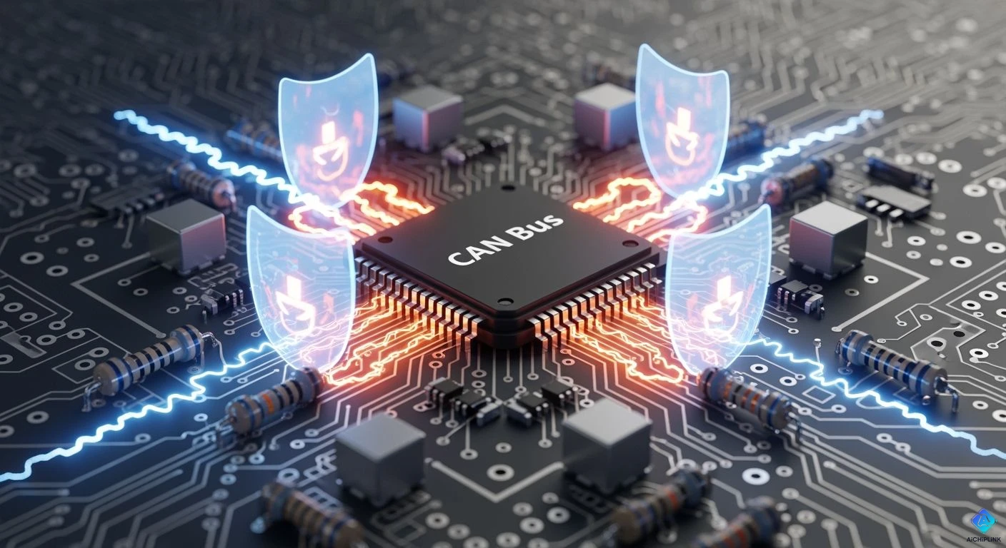
Put a two-line bidirectional TVS diode array right beside your connector. Combine this array with a common mode choke and current-limiting resistors. This setup offers quick temporary surge blocking before electrical noise touches your sensitive transceiver.
Creating strong CAN bus protection designs keeps high-speed car systems safe from damage. Correct ESD protection prevents physical breakdown. Modern car CAN bus hardware needs a careful layout. This guide covers picking parts, improving PCB trace paths, and following ISO 10605, ISO 7637-2, and IEC 61000-4-2 rules. Add reliable circuit protection to guard your complex CAN bus systems up to 5 Mbps against sudden ESD spikes in any working vehicle setup.
Key Takeaways
-
Put TVS diode arrays close to the primary connector to quickly stop sudden power surges.
-
Pick low-capacitance TVS diodes to help high-speed CAN bus data signals stay clear and sharp.
-
Route pairs of signal wires with exact matching shapes to block unwanted electrical noise and bouncing signals.
-
Check circuit board designs using scope eye diagrams to ensure dependable car network signals.
Standards for Automotive CAN Bus Transient Stress
Every car CAN bus transceiver needs protection against fast electrical spikes. Big voltage jumps reach car wires when people touch them or switches flip. Because of this, you must follow clear safety rules to build strong protection circuits.
ISO 10605 and IEC 61000-4-2 ESD Ratings
Car parts must pass static electricity tests to ensure they run well after hard electrical shocks. The iec61000-4-2 standard tests static discharge using one resistor-capacitor setup of 330Ω and 150pF. ISO 10605 tests four different setups by mixing two resistors (330Ω, 2000Ω) with two capacitors (150pF, 330pF).
-
IEC 61000-4-2 Limits: Checks top voltage levels up to ±8kV for direct contact and ±15kV through the air.
-
ISO 10605 Limits: Increases air discharge testing up to ±25kV for components people touch from the outside.
-
Repetition Rates: ISO 10605 requires 10 shocks each second, but IEC 61000-4-2 calls for 20 shocks each second.
-
Grounding Setup: ISO 10605 sets the test item on a metal flat surface that acts like the car frame.
Learning these differences helps you select ESD parts that control voltage levels correctly.
Transients and Differential Bus Voltage Limits
Normal driving creates dangerous voltage spikes along the wiring bundle. ISO 7637-2 describes destructive power surge events. Pulse 1 acts like negative voltage spikes from turning off inductive items. Pulses 2a, 3a, and 3b act like positive switching spikes in the wire bundle. ISO 16750-2 describes load dump stress when a battery unhooks while the generator makes power.
ISO 16750-2 load dump events create long high-power surges that quickly ruin unprotected transceiver chips.
Your surge protection circuit must handle voltage differences across lines during fast battery jump-starts. Mechanics frequently attach two batteries that send 24V right into 12V system wires. Bad wiring can also put backward battery voltage across CAN_H and CAN_L wire paths. Strong hardware setups keep unwanted current small during these constant DC power faults. Good surge parts squeeze incoming voltage spikes below chip danger limits, keeping fragile microchips safe from lasting damage.
Component Selection for ESD Protection
TVS Diode Array Parameter Matching
You need to pick a two-line bidirectional TVS diode array to clamp sudden voltage spikes on lines. Choose TVS parts with a standoff voltage above 24V or 32V. This extra margin keeps diodes from turning on during battery jump-starts or vehicle power surges. Special parts like the CDSOT23-SM712 safeguard transceivers that handle uneven voltage differences between far-apart ground points.
Modern high-speed CAN-FD communication requires smart handling of bus load. Regular diodes add extra capacitance that bends fast signal shapes. Choosing ultra-low-capacitance silicon keeps signal edges sharp and clean over long wires. You must check total load limits before picking your final TVS array.
In every CAN bus protection design, a TVS diode placed near the connector must have a junction capacitance of less than 10 pF. It is critical to strictly control the total node capacitance to maintain signal integrity.
Common Mode Chokes and Inline Elements
You can put a common mode choke between the TVS array and your transceiver pins. This choke blocks high-frequency noise while letting main data signals pass through smoothly. Fast voltage spikes will not ruin soft transceiver chips when you pick strong filters made for cars.
| Parameter | Value |
|---|---|
| Part Number | CM1210C113R-1A |
| Application | Automotive CAN-Bus Common Mode Choke |
| Inductance | 11.00 µH (at 100 kHz) |
| Rated Current | 0.300 A (max) |
You can also place inline resistors or resettable fuses in a row with your CAN wires. These inline parts block heavy fault currents whenever power shorts happen on the car wiring bundle. Good component choices keep your hardware working well under harsh driving conditions.
Mixing simple inline parts with clamping arrays builds a full safety system. The common mode choke filters noise while the TVS diodes absorb static shocks. This setup offers strong esd protection without slowing down your fast network speed.
CAN Bus Protection Design and PCB Layout
Component Placement Sequence and Routing Rules
Follow a strict physical layout sequence on your circuit board. Place components along the signal path starting from the main entrance connector. Position the TVS diode array right beside the board edge entry point. Route the differential lines directly into the common mode choke pins. After the choke, place termination resistors right before the transceiver pins. This setup offers transient protection by stopping high energy before it touches sensitive silicon. Proper hardware placement keeps high-frequency noise from spreading into quiet board regions. Solid can bus protection design relies on this exact sequence.
Keep complete physical symmetry across CAN_H and CAN_L traces. Route equal line lengths directly through each device to keep the pair balanced. Keep your trace paths short and wide between the entry connector and the TVS pads. Short, wide traces minimize parasitic trace inductance during fast transient risetimes.
Ground Return Paths and Parasitic Reduction
Your TVS array requires a strong, low-impedance return path to divert heavy current safely. Connect the TVS ground pins directly to a continuous ground plane or chassis ground screw. Place grounding vias right next to the component landing pads. Broad ground connections stop dangerous voltage spikes by draining surge currents quickly into the ground layer. Implementing proper esd protection preserves signal quality and protects components against static discharge.
Avoid creating stub traces on high-speed differential signal lines. Stubs cause sharp impedance changes that reflect signal waves back into the transceiver. SAE J1939/11 limits single stub lengths to 1 meter maximum, but optimal board designs avoid stubs completely. Unplugged stubs cause bad edge ringing and delay signal settling times during data frames. You complete a top-performing can bus protection design by keeping all differential signal routing clean and straight.
Transient Protection Validation and Compliance
Testing Protocols and Signal Integrity
You must test surge protection success after placing parts on your circuit board. First, check all connections for loose wires, damage, or rust. Next, turn off circuit power completely. Use a multimeter to measure differential resistance across CAN High and CAN Low wires.
| Measured Resistance | Network Condition & Performance Impact |
|---|---|
| ~55 to 65 Ohms | Reliable communication and optimal network performance. |
| 30 to 50 Ohms | Communication reliability is degraded. |
| 110 to 140 Ohms | Increased likelihood of communication errors. |
| >10 MOhms | Communication becomes impossible. |
Check for shorts by measuring resistance between each line and ground. Both checks must read very high. Connect a fast scope to view live bus signal shapes. The scope displays voltage drops, noise spikes, and signal distortions. Next, review error logs using test software. Unplug individual nodes one by one to locate bad hardware. These tests prove that your esd parts protect signal quality during fast spikes.
Eye Diagram and Compliance Inspection
You prove full network compliance by showing differential signals inside a scope eye diagram window. The eye diagram uses a 6-point mask that creates a clear clear-out area for the signal wave. Signals fail testing right away if any trace crosses this middle mask space.
Vertical mask walls check voltage height against minimum receiver input limits. Regular tests check dominant-bit-low signals between -0.9 V and -0.5 V. Otherwise, tests check dominant-bit-high signals between +0.5 V and +0.9 V. Horizontal mask walls check timing errors, system jitter, clock shifts, and signal delay times. Extra circuit protection keeps differential signals clean and stops errors across your car network.
You can finish your board layout successfully by following this final design checklist:
-
Put two-way TVS diodes right next to the main connector to block quick voltage spikes.
-
Wire TVS ground pins straight to a wide, low-resistance circuit board ground layer.
-
Pick TVS diodes with high standoff limits and low inner capacitance to keep signals clear.
Run full end-of-design tests before sending your car CAN bus safety circuit in for official EMC testing. Look at differential eye diagrams to check signal voltage levels and bit timing limits. Use time-domain reflectometry tools to spot hidden resistance changes along the board traces. These testing steps confirm strong ESD protection and guarantee steady transceiver operation across busy car networks.

Written by Jack Elliott from AIChipLink.
AIChipLink, one of the fastest-growing global independent electronic components distributors in the world, offers millions of products from thousands of manufacturers, and many of our in-stock parts is available to ship same day.
We mainly source and distribute integrated circuit (IC) products of brands such as Broadcom, Microchip, Texas Instruments, Infineon, NXP, Analog Devices, Qualcomm, Intel, etc., which are widely used in communication & network, telecom, industrial control, new energy and automotive electronics.
Empowered by AI, Linked to the Future. Get started on AIChipLink and submit your RFQ online today!
Frequently Asked Questions
Why must you place the TVS diode array directly next to the connector?
Put the TVS diode array beside the connector to block sudden voltage jumps right away. This layout stops strong electric surges from moving across your board wiring. Fast blocking protects the common mode choke and transceiver chip from static electricity damage.
What maximum junction capacitance should you select for CAN-FD TVS diodes?
Pick a TVS diode with a junction capacitance below 10 pF for CAN-FD systems up to 5 Mbps. Higher capacitance distorts fast signal shapes over the wires. Low capacitance keeps bit edges sharp and clear across your network lines.
Why do you need common mode chokes alongside TVS diodes?
TVS diodes stop big voltage spikes from static shocks. Common mode chokes filter high-frequency noise out of differential wires. Working together, these parts give total esd protection while keeping fast data signals clean across car networks.
How do you prevent signal reflections on high-speed CAN traces?
Route CAN_H and CAN_L wires as matching pairs without extra line stubs. Unused stubs create resistance shifts that bounce signal waves back. According to SAE J1939/11, clean wire paths stop edge ringing and prevent data timing errors.