How to Choose the Right Comparator IC for Circuit Designs

You rely on a comparator ic to check two smooth analog inputs and create a clear digital output. Modern circuit design needs exact trigger points so systems can run reliably. You must carefully look at key choices like reaction speed, power use, signal gain, small voltage errors, and output setups. Classic parts like the lm339 comparator ic show how certain designs decide your pull-up resistor needs. The industry shows massive growth for these special parts:
Digital Comparator ICs Market size was valued at USD 1.23 Billion in 2024.
Picking the right comparator stops accidental signals and improves total energy efficiency.
Key Takeaways
-
Pick the right response speed and propagation delay to fit your system's timing needs.
-
Pick open-collector outputs like the LM339 for changing voltage levels, or choose push-pull outputs for high-speed switching.
-
Add positive feedback to your comparator to create hysteresis and prevent noisy signals from making the output jump rapidly.
-
Choose very low-power comparator chips and tiny packages to help save battery life and space.
Key Parameters for Comparator IC Selection
You must check important electric factors while planning your electronic systems. These values show how well your sensor circuit spots tiny continuous voltage shifts and outputs dependable digital signals.
Response Speed, Propagation Delay, and Open-Loop Gain
Response speed measures how fast the output flips logic states when an input signal crosses a set limit. Signal lag measures this exact reaction duration. You need to compare signal lag with your system timing rules to avoid random logic mistakes. Battery-saving builds change state slowly to preserve power, whereas fast sensor setups need sub-nanosecond reaction times.
| Comparator Type | Propagation Delay Range | Specific Examples from Source |
|---|---|---|
| Low-Power Comparator | Up to 70 µs | A low-power comparator may take 70 µsec to switch. |
| High-Speed Comparator | 150 ps to 7 ns | LMV7219 has a 7-nsec delay. LT1719 and LT1715 have 4-nsec delays. |
Combining a wide supply range with ultra‑low power consumption and a fast 60 ns propagation delay, the TS3121P delivers accurate, high-speed threshold detection.
High internal signal amplification boosts tiny input variations, shifting the output quickly between power limits. This strong boost sharpens output changes whenever input signals drift slowly past trigger levels. Designers find the highest allowable signal lag inside a system through a standard route checking method:
-
Path Separation: You split your digital network into simple timing lines from starting clocks to ending points.
-
Delay Counting: You sum up total signal lag by adding all single switch delays and wire path delays.
-
Slow Path Finding: You review all timing lines to find the longest route for setup tests and the shortest route for hold tests.
-
Limit Testing: You check the total worst-case signal lag against your required clock cycle and setup timing rules.
-
Error Checking: You judge if the route signal lag satisfies timing rules or creates a timing error.
Input Offset Voltage and Operating Range
Input offset voltage is the natural voltage difference found directly across the input pins. You must add a small fix voltage across these pins to balance the inner input section. Using an op amp comparator often adds large offset voltage, which hurts trigger point accuracy. By contrast, a real comparator chip offers factory tuning or auto-zeroing to reduce voltage mistakes. Though older parts like the lm339 comparator ic work fine in simple level sensing designs, high-precision projects demand lower input offset limits.
| Comparator Type | Typical Input Offset Voltage | Typical Offset Voltage Drift |
|---|---|---|
| Standard / General-Purpose Comparator | ~2 mV | 5–15 μV/°C |
| Precision / Zero-Drift Comparator | 1–5 μV (maximum) | 0.01 μV/°C |
Exact zero-drift chips constantly track and erase input voltage errors with chopper-stabilization methods. For instance, a 5 μV offset in a circuit using a 5.000V base leads to a 0.0001% trigger mistake. This super tiny mistake allows lab-grade measuring precision inside sensitive sensor setups.
You should also check the allowed shared input voltage range while picking your parts. Running outside this safe zone can cause signal flipping, leading to bad logic mistakes at the output end. Flexible four-channel parts, like the lm339 comparator ic, need careful wire paths within given power lines. Choosing a good comparator chip ensures steady switching action across all working temperature ranges and power levels.
Output Topologies and the LM339 Comparator IC
Open-Drain and Open-Collector Configurations
Picking the right output stage is essential when planning your circuit layout. Many classic parts use open-collector or open-drain setups for extra system choices. The basic lm339 comparator ic works as a standard open-collector output component. You need an external pull-up resistor to pull your output signals high. An inner open-collector NPN transistor pulls the pin low to ground while active.
| Specification | Key Value/Feature | Relevance to Open-Collector Designs |
|---|---|---|
| Output Type | Open Collector | Enables wired-AND logic and custom pull-up voltage matching. |
| Supply Voltage Range | 2V to 36V | Supports broad operating power environments. |
| Output Saturation Voltage | 130 mV at 4.0 mA load | Minimizes active-low voltage loss and power dissipation. |
| Package Options | 14-pin PDIP, SOIC, TSSOP | Offers flexibility for diverse board layouts. |
You can join outputs together with the lm339 comparator ic to create wired-AND logic tasks. Connecting different digital logic families is easy when using the lm339 comparator ic. A pull-up resistor ties the output pin right to your picked logic power level. For instance, run the chip on a high supply while fixing pull-up voltage at 5V or 3.3V for TTL and CMOS inputs.
The external resistor lifts output up to digital supply voltage when the inner output transistor inside the lm339 comparator ic stops conducting. The active output transistor sinks power straight down to ground upon reaching saturation. Sinking around 5 mA of current, the lm339 comparator ic shows a low normal saturation voltage near 0.2 V. Figure out the load current through a connected load using a basic formula: load current = (supply voltage - load voltage - saturation voltage) / pull-up resistance. A 5 V supply, a 2.0 V LED forward voltage, a 0.2 V saturation voltage, and a 3.3 kΩ pull-up resistor yield a calculated current of roughly 2.8 mA. The lm339 comparator ic manages these connected loads smoothly across every single board package. You can rely on the lm339 comparator ic for solid level shifting between different voltage setups. Every open-collector comparator uses this passive pull-up method to set up the high logic state.
Push-Pull Stage Selection for High-Speed Logic
A high-speed ic comparator frequently employs a push-pull output setup instead of an open-collector stage. Internal transistors inside a push-pull comparator stage supply both active pull-up and active pull-down actions. This active totem-pole layout gets rid of the demand for any outer pull-up resistor. Fast digital systems gain quick switching changes by using a push-pull comparator.
| Output Type | Speed/Edge Rate | Typical Application | Key Reason for Speed Advantage |
|---|---|---|---|
| Push-Pull | Faster switching, produces faster edge rates. | Point-to-point or unidirectional interfaces (e.g., SPI, UART). | Actively sources and sinks current with a pair of transistors. |
| Open-Drain | Slower rise times, limited by RC delay. | Shared bidirectional buses. | Relies on external pull-up resistor to pull signal high. |
Signals are actively driven close to both power rails by a push-pull comparator stage. Current comes from the upper transistor to push the signal high. Current sinks through the lower transistor to pull the signal low. This double action removes RC delays from line capacitance and external pull-up resistors. Select a push-pull comparator ic for direct, high-speed logic lines such as SPI or UART layouts. However, use the open-collector output of the lm339 comparator ic when building shared buses or changing voltage levels. Choosing a push-pull comparator gives you sharp signal shifts without adding extra passive parts.
Noise Immunity and Detection Logic in Circuit Design
Internal and External Hysteresis Implementation
You must shield your circuit build from signal noise inside industrial spaces. Workplace setups bring noise through magnetic interference, power ripple, and sensor lines. Device noise creates rapid output chatter when inputs stay within 1 mV to 2 mV of limits. For instance, 2 mV of input noise adds 1 μs of timing jitter to 60 Hz signals.
| Hysteresis Type | Implementation Method | Threshold Formula | Example Resistor Values |
|---|---|---|---|
| External Positive Feedback | Connect feedback resistors between output and non-inverting input | Hysteresis = VOH × (R1 / (R1 + R2)) | R1 = 10 kΩ, R2 = 90 kΩ |
Adding positive feedback builds a safe gap that stops output chatter. You set the upper limit using VTH = VREF + (VOH - VREF) × (R1/(R1+R2)). You set the lower limit using VTL = VREF + (VOL - VREF) × (R1/(R1+R2)). For example, getting 500 mV hysteresis from a 5 V high output needs an R1 to R1 plus R2 ratio of 0.1. Picking R1 = 10 kΩ and R2 = 90 kΩ meets this ratio for your comparator ic. Wiring feedback across an lm339 comparator ic stabilizes your switching points.
Single Threshold Detection versus Window Detection
A single limit detector uses one comparator to check signal levels. You feed a fixed reference voltage to one input pin while routing your signal to the other. The output shifts state whenever the input passes that set reference point. You can build this simple voltage check circuit using an lm339 comparator ic.
A standard voltage comparator determines if a signal is higher or lower than a single reference point. A window comparator circuit uses two comparators to create an in-range logic output when the input sits between two thresholds.
A window detector uses two comparators plus a logic gate to check a voltage zone. One comparator checks if the signal rises past the bottom edge. The second checks if it drops below the top edge. An AND gate joins both signals to output a logic high only when the input stays safe inside the zone. Using two channels on an lm339 comparator ic with an ic comparator setup gives clear range checks across your board.
Power Constraints and Package Selection
Ultra-Low-Power Architectures for Battery Systems
You should check idle current when building portable gear. Battery-run setups need very low power draw during resting times. Pick a low-power comparator ic to save battery power.
Low-power comparators (IQ/ch < 10 µA) Power-efficient comparators with quiescent current as low as 75 nA for extending battery life.
Using a tiny-power comparator ic increases device runtime by a lot. Compare normal idle current levels across common choices:
| Comparator Type / Model | Typical Quiescent Current (I_Q) |
|---|---|
| Ultra-Low-Power (TLV7031) | 315 nA |
| Ultra-Low-Power (TLV3701) | 560 nA |
| Typical Micropower (e.g., MAX919) | ~1,200 nA (1.2 µA) |
| Standard (LM393, per channel) | ~200,000 nA (200 µA) |
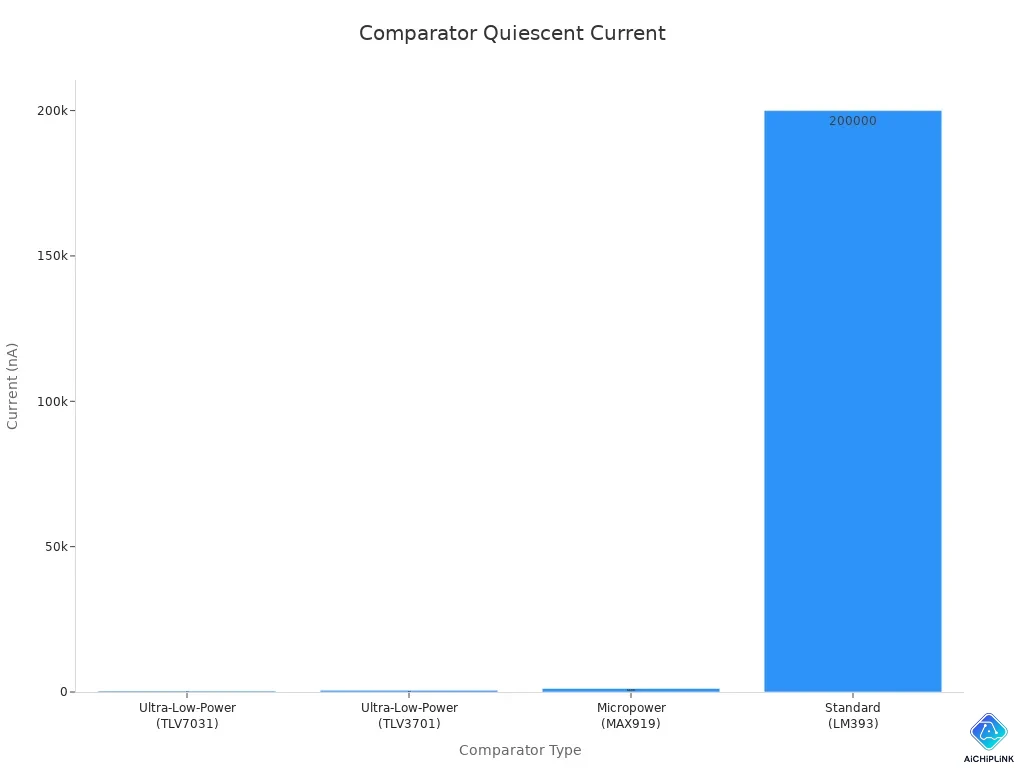
Older chips draw a lot of power while running constantly. Switching standard chips for dedicated single-channel parts saves big battery life. The classic lm339 comparator ic uses more supply current per channel. Modern battery monitors work better with a dedicated micropower comparator chip instead.
Thermal Limits and Package Footprint Optimization
Chip size changes heat control and open board space. Small modern designs need clever layout choices.
| Aspect | SOT-23 Package | SC-70 / SOT-323 Package |
|---|---|---|
| Typical Thermal Resistance (θJA) | ~300 °C/W | Lower thermal mass limit |
| Relative Footprint Size | Larger, general-purpose size | Requires ~2.1 x 2.0 mm footprint |
| Current Handling Capability | Up to ~600 mA | Up to ~600 mA |
| Primary Design Trade-off | Easy hand-soldering for prototyping | Superior for high board density |
The SOT-23 chip size has a normal heat resistance of ~300 °C/W. The tiny SC-70 package uses a small ~2.1 x 2.0 mm footprint. Both options manage power handling levels up to ~600 mA. Smaller chips release less overall heat during heavy power changes.
Pick chip shapes based on real board building steps. Bigger surface-mount options make hand soldering simple during early testing. Packed consumer gear needs tiny SC-70 packages to save room. Use the classic lm339 comparator ic in DIP or SOIC shapes for basic breadboards. Good package choices balance heat control, build costs, and small shapes in your full design.
You can create solid circuits by looking at four basic design rules:
-
Check signal lag against your main timing limits to keep parts running smoothly.
-
Pick an open-collector style like the classic lm339 comparator ic for mixed voltages, or use push-pull for fast signals.
-
Put in feedback loop wiring to stop unwanted noise and prevent shaky switching mistakes.
-
Review continuous standby power to hit your low-energy battery targets.
You must study component data sheets under harsh temperature shifts and power supply limits. Checking these tough conditions guards your circuit layout against sudden trigger point changes. Finish your circuit board plan only after checking these performance limits in real working conditions. Every chip choice directly affects how well your final device works.

Written by Jack Elliott from AIChipLink.
AIChipLink, one of the fastest-growing global independent electronic components distributors in the world, offers millions of products from thousands of manufacturers, and many of our in-stock parts is available to ship same day.
We mainly source and distribute integrated circuit (IC) products of brands such as Broadcom, Microchip, Texas Instruments, Infineon, NXP, Analog Devices, Qualcomm, Intel, etc., which are widely used in communication & network, telecom, industrial control, new energy and automotive electronics.
Empowered by AI, Linked to the Future. Get started on AIChipLink and submit your RFQ online today!
Frequently Asked Questions
What is the main difference between an op amp and a comparator?
An op amp works inside continuous linear feedback loops. Meanwhile, a comparator checks two input voltages and flips the output quickly between limits. Picking a real comparator stops output delay and prevents simple logic mistakes in your designs.
Why does the lm339 comparator ic require an external pull-up resistor?
The classic lm339 comparator ic uses an open-collector output stage. An inner transistor pulls the output pin straight down to ground. You must add an outer pull-up resistor to pull the output high when the inner transistor turns off.
How do you choose between push-pull and open-collector output architectures?
Choose a push-pull comparator for fast digital signals like SPI or UART lines. Push-pull parts drive signals both ways without extra pieces. Select an open-collector chip like the lm339 comparator ic to join different logic voltages or build wired-AND networks.
Why should you add positive feedback to a comparator?
Signal noise makes the output flip rapidly near limit points. You fix this issue by adding positive feedback to your comparator. This extra path sets clear high and low trigger points, keeping your output steady when inputs move slowly.
Can you run the LM339 on a single power supply?
Yes, you can run the lm339 comparator ic on one power supply from 2V to 36V. The chip works safely across this wide power range, making it a great choice for flexible factory equipment.