Comparing Source Drivers vs Gate Drivers in Display Driver IC Architecture
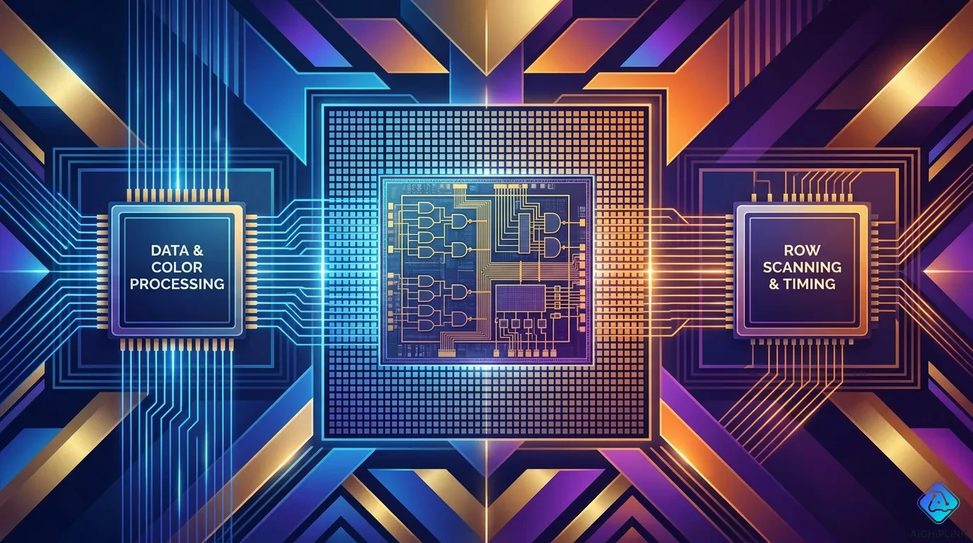
Modern Display Driver IC systems split screen control into two main microchip parts. Source drivers, also called column drivers or data drivers, send exact analog pixel voltage or current levels. These steady signals set correct brightness values along vertical control lines. Gate drivers, also known as row drivers or scan drivers, create timed high-voltage signals. They turn on horizontal control lines one after another in order. This action opens a short time window for pixels to charge with incoming column data. Dividing the system this way keeps harsh high-voltage power jumps away from sensitive, accurate signal paths. Gate drivers use big voltage shifts to turn small panel transistors on and off. Meanwhile, source drivers use smart digital-to-analog converters to keep the pixel voltage completely accurate.
Key Takeaways
-
Source drivers control column brightness, while gate drivers turn horizontal pixel rows on and off.
-
Gate drivers use high power to quickly turn on the pixel switches on the screen.
-
Gate-on-Array technology builds row drivers directly onto glass, which helps create much thinner screen borders.
-
Fast source drivers quickly change pixel power levels to keep screen colors looking crisp and correct.
Architecture Overview of Display Driver IC Types
Source Driver Column Operations
Source drivers control how correct analog target voltages travel down vertical data lines on the display panel. A central digital controller sends multi-bit pixel brightness numbers straight into the inner registers of the driver chip. Digital-to-analog converters then turn these binary data inputs into clear, highly accurate voltage signals. Modern panels connect one dedicated source channel to every single physical column line. These channels continuously send changing voltage levels to set brightness values for each individual pixel sub-pixel.
Fast digital switching inside the chip routes reference voltages through resistor networks into output operational amplifiers. These low-impedance buffer amplifiers push the created voltage levels out onto capacitive matrix lines. Quickly charging the long vertical line capacitance forces the line voltage to settle fast inside the given line time. Exact analog voltage control directly changes liquid crystal rotation or organic light-emitting diode current flow. As a result, source drivers build the full grayscale range and overall color accuracy across the visual screen.
Gate Driver Row Selection
Gate drivers handle the horizontal timing of the matrix panel. A shift register chain passes one selection pulse through neighboring row outputs in a set order. Level shifters boost low-voltage digital clock signals up to high working panel voltages. The higher positive voltage opens thin-film transistors along a whole active horizontal line at the same time. This starting step switches on every pixel control gate in that specific row.
Opening the pixel transistors opens a set time window for data transfer. Liquid crystal capacitors and pixel storage nodes catch analog voltage values from active vertical data lines while open. The driver then moves the selection pulse to the next row and drops the previous gate line voltage down to a negative bias level. This negative voltage turns off the pixel transistors completely. Strong OFF-state isolation locks the saved pixel charge in place until the next refresh cycle arrives. The shared work inside the Display Driver IC system guarantees clean screen updates without data loss.
Voltage Domains and Signal Integrity
Analog Settling in Source Drivers
Source drivers work mostly in low and medium voltage ranges to save overall electrical power. Inside the chip, digital logic runs on low core power, while output amplifiers use medium analog supply lines. Digital control parts smoothly move grayscale data through inside storage slots. These drivers need to send exact analog voltage levels to thousands of separate channel outputs at once. Quickly charging heavy display columns needs careful signal speed control during short line timing windows.
Fast voltage settling directly controls final pixel voltage accuracy right before the row transistor turns off. Built-in output buffer circuits must quickly stop voltage bouncing to prevent ugly lines across the visual screen. Quick signal settling stops unwanted line-to-line electrical noise when brightness voltages change fast. Design engineers keep tweaking buffer power strength to preserve clear, strong signals across long display wire paths.
High-Voltage Swings in Gate Drivers
Gate drivers need much higher working voltage levels than source drivers to turn panel switches on and off reliably. Glass display transistors inside large LCD screens need strong electric fields to turn on easily with low resistance. High-voltage level shifters raise low-voltage digital timing pulses into high-voltage row selection signals. The driver channels then send these boosted pulses down heavy row wire lines.
| Parameter | Value |
|---|---|
| Gate High Voltage (Vgh) | +15V to +25V |
| Gate-Source Voltage ON (Vgs(ON)) | +10V to +15V |
These big voltage jumps create heavy electrical noise that spreads into nearby screen layers. High power surges flow through the main power lines while active row lines update. Negative OFF-state voltage levels stop extra electrical leaks through turned-off pixel switches. The large voltage gap between high-voltage gate lines and sensitive data lines stresses inner chip isolation spaces. Layout engineers put wide physical shield rings around high-voltage pins to protect nearby low-voltage signal paths well.
Circuit Topologies in Display Driver IC Design
Chip engineers pick different circuit designs to manage analog accuracy and high-voltage power on a screen. The inner structure divides component space, work blocks, and overall layout shapes between data control and row scan jobs.
R-DAC and Buffer Configurations
Source driver channels rely heavily on resistor-string digital-to-analog converters (R-DACs) and operational amplifiers. Multi-channel source chips must send fine voltage steps to every vertical data line at the same time. A high-resolution R-DAC uses long series strings of matched poly-silicon resistors to divide main reference voltages into exact grayscale points. Multiplexer switches then pick the right voltage based on digital input codes from core memory registers.
The chip space for these resistor networks grows very fast with higher screen color depth. Designers fit thousands of matched resistor parts into narrow chip spaces to keep outputs uniform across all channels. Operational amplifier buffers connect directly to these decoder output lines. Each output channel uses its own unity-gain operational amplifier to drive heavy column line capacitive loads.
| Circuit Component | Architectural Function | Silicon Area Impact |
|---|---|---|
| R-DAC Resistor Ladder | Generates precise grayscale reference voltages | Dominates analog floorplan footprint |
| Multiplexer Switches | Routes selected voltage to channel buffer | Scales with digital bit resolution |
| Operational Amplifier | Drives high column line capacitance | Requires stable bias current networks |
These operational amplifiers use wide input transconductance stages and push-pull output transistors. The amplifier design balances low idle power use with strong peak drive power. Fast signal settling needs a quick current response without making bad voltage bounces across long display wires. Engineers add frequency compensation capacitors to keep the feedback loop stable while driving active display panels.
Shift Registers and Level Shifters
Gate drivers use a very different layout pattern compared to source drivers. Instead of big analog resistor grids and steady-voltage buffers, gate driver blocks mostly use digital logic chains and high-voltage connection circuits.
A chain of static D flip-flops forms a continuous shift register line across the chip length. Clock pulses push one active HIGH state from one register step to the next step in precise order. Each register output turns on the next line control block, creating the smooth scanning pattern needed for row selection. Logic gate delays inside each register step match the main system refresh rate.
High-voltage level shifters connect low-voltage shift registers to high-voltage output drivers. Standard low-voltage CMOS logic cannot handle the large voltage gaps needed to turn thin-film panel transistors fully on or off. Level shifters use cross-coupled high-voltage PMOS and NMOS transistor pairs to turn low-voltage timing signals into high-power output pulses.
These level-shifting circuits need special chip layout methods to manage big voltage gaps without burning out inner chip insulation. Layout engineers add thick gate oxides and extended drain spaces to high-voltage transistors inside the output path. Guard rings surround level shifter cells to block electrical noise from reaching nearby digital logic blocks. This circuit layout cuts down unwanted current leaks while keeping clock timing signal edges clean and sharp. Modern Display Driver IC designs divide chip space between dense analog converters for data lines and strong high-voltage logic for row selection.
Power Integrity and Dynamic Noise
Column Crosstalk and Power Noise
Quick signal changes across crowded vertical channels cause strong noise inside the source driver chip. Fast digital lines flip at once to update neighboring pixel columns. Unwanted capacitance between close metal wires pushes these fast voltage changes into nearby data lines. This unwanted coupling changes target analog voltages before display pixels lock in the charge. Designers protect sensitive analog outputs with grounded shield wires to keep signals clear.
Many switching outputs also pull sudden power jumps from the main power lines. These power jumps make voltage drops across the inner power delivery paths. Changing power lines lowers the accuracy of output amplifiers and resistor networks. Engineers put small capacitors near amplifier power pins to keep local voltage steady. This local power supply stops voltage bouncing and keeps accurate grayscale colors.
Gate Line RC Propagation Delays
Horizontal scan lines have high wire resistance and capacitance across the whole display glass. Gate drivers send high-voltage control pulses through these long, thin metal wires. Joined wire resistance and spread-out capacitance create large signal time delays. These delays change sharp square clock pulses into sloped, rounded voltage shapes at the far screen edge.
Slow voltage rise and fall times shorten the open pixel charging time at the far screen edge.
Different pulse shapes cause clear brightness changes between the driver side and the far side screen edge. Transistors far from the gate driver turn on slowly and turn off late. This late switching lets column data leak into nearby pixel rows during fast screen refreshes. Engineers use two-sided gate drivers or better wire sizes to lower total timing delays across large displays.
Modern Display Integration Trends
Gate-on-Array Integration
Screen makers now put row drivers right onto the display glass surface. Engineers call this design Gate-on-Array technology. Thin-film transistors on the glass create scan circuits along the outer edges of the screen. These glass circuits replace extra microchips for horizontal line control. They get timing signals straight from the main display board without separate gate driver chips.
Removing extra row chips makes outer screen borders much smaller. Screen factories build scan circuits and pixels at the same time on the glass. This process saves money and removes delicate ribbon cable connectors. But glass transistors have lower power performance than silicon chips. Designers make these glass transistors wider to push enough current down long panel rows.
High-Refresh Rate Source Drivers
Modern gaming displays need high frame rates to show smooth motion without blur. Faster refresh rates leave less time to charge pixel storage capacitors. A modern Display Driver IC must handle data quickly without losing voltage accuracy. Internal digital lines send pixel codes to memory slots at fast clock speeds. Fast data delivery ensures quick voltage updates across all vertical data lines.
Output buffers need wider bandwidth to settle voltages in short time windows. Engineers design advanced display amplifiers that control their own power use. Higher starting current speeds up line charging when voltages change. The amplifier then lowers its current draw while holding steady voltage levels. This smart power use keeps color accurate while reducing heat in slim devices.
Display Driver IC architecture balances exact analog voltage outputs and strong high-voltage timing pulses. Source drivers focus on channel output precision to set grayscale levels correctly. Gate drivers manage high-voltage switches to open row selection windows sequentially across the screen matrix.
Engineers designing for advanced OLED, LTPS, and MicroLED panels must optimize both driver types carefully. Fast-refresh LTPS displays need high-bandwidth source buffers to reduce analog settling times. Direct-emission OLED and MicroLED systems require tight gate pulse control and robust isolation to prevent brightness variations. Matching line impedance across all control lines ensures reliable system integration and uniform pixel performance.

Written by Jack Elliott from AIChipLink.
AIChipLink, one of the fastest-growing global independent electronic components distributors in the world, offers millions of products from thousands of manufacturers, and many of our in-stock parts is available to ship same day.
We mainly source and distribute integrated circuit (IC) products of brands such as Broadcom, Microchip, Texas Instruments, Infineon, NXP, Analog Devices, Qualcomm, Intel, etc., which are widely used in communication & network, telecom, industrial control, new energy and automotive electronics.
Empowered by AI, Linked to the Future. Get started on AIChipLink and submit your RFQ online today!
Frequently Asked Questions
What is the main structural difference between source drivers and gate drivers?
Source drivers use resistor chains and amplifier circuits to send steady voltage levels down vertical screen lines. Gate drivers use timing logic and power boosters to pass strong timed signals down horizontal scan lines.
Why do gate drivers require much higher operational voltages than source drivers?
Gate drivers need to open and close small panel switches completely on the screen glass. Strong positive power reduces line resistance during row updates. Negative power turns off switches tightly to stop extra energy leaks between screen refreshes.
How does Gate-on-Array technology change display architecture?
Gate-on-Array technology builds scan control parts right on the glass using thin-film transistors. This design gets rid of separate row chips and soft connector strips. As a result, screen makers build displays with much thinner frame borders.
What causes analog signal settling issues in high-refresh-rate displays?
Faster refresh rates give each row line much less time to charge up. Heavy line capacitance and wire resistance slow down voltage changes. Source driver amplifiers must push more power quickly to set correct screen voltages before switches turn off.