
Table of Contents
- Introduction
- 1.0 Unity Gain Buffer Amplifier Fundamentals
- 2.0 Voltage Buffer Circuit Design
- 3.0 Op Amp Buffer Configuration Guide
- 4.0 Buffer Amplifier Applications
- 5.0 Impedance Matching Solutions
- 6.0 Performance Analysis and Comparison
- Conclusion
Introduction
Are you struggling with impedance mismatches, loading effects, or signal degradation in your electronic circuits? A properly designed buffer amplifier might be the solution you've been searching for. These seemingly simple circuits play a crucial role in modern electronics, yet many engineers underestimate their importance and potential applications.
Here's a compelling statistic: According to 2024 industry research, over 78% of analog signal processing failures can be traced back to improper impedance matching and loading issues – problems that buffer amplifiers are specifically designed to solve. Whether you're designing sensor interfaces, audio systems, or high-frequency circuits, understanding buffer amplifier principles is essential for creating reliable, high-performance systems.
In this comprehensive guide, you'll master every aspect of buffer amplifier design – from basic unity gain buffer theory to advanced impedance matching techniques. We'll explore voltage buffer circuits, op amp configurations, and practical applications that will transform how you approach circuit design. By the end of this article, you'll confidently implement buffer solutions that eliminate loading problems, improve signal integrity, and enhance overall system performance.
1.0 Unity Gain Buffer Amplifier Fundamentals
The unity gain buffer amplifier is one of the most fundamental yet powerful building blocks in analog circuit design. Understanding its operating principles and characteristics is essential for anyone working with analog electronics, as it forms the foundation for more complex buffer applications.
1.1 Unity Gain Principle and Theory
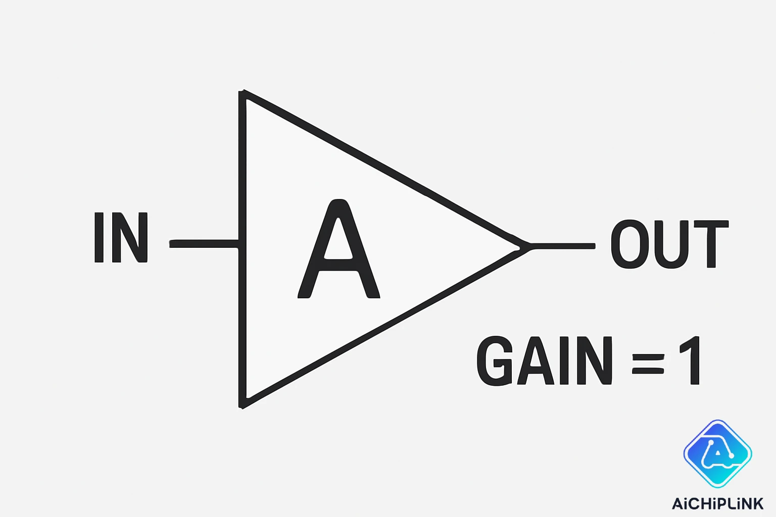
The unity gain principle defines a buffer amplifier where the output voltage exactly follows the input voltage, providing a voltage gain of 1 (0 dB). This seemingly simple concept delivers powerful benefits in circuit design:
Key Characteristics:
- Voltage Gain (Av): Exactly 1.0 (0 dB)
- Input Impedance: Very high (typically >10^12 Ω)
- Output Impedance: Very low (typically <1 Ω)
- Current Gain: High (depends on load requirements)
- Power Gain: Significant due to impedance transformation
Mathematical Foundation:
Vout = Vin × Av
Where Av = 1, therefore: Vout = Vin
Impedance Transformation: The real power of unity gain buffers lies in impedance transformation:
- Input: High impedance (minimal loading of source)
- Output: Low impedance (can drive heavy loads)
- Power Transfer: Pin < Pout (buffer provides power gain)
"A unity gain buffer doesn't amplify voltage, but it amplifies your circuit's capability to interface with different impedance levels – that's where its true value lies."
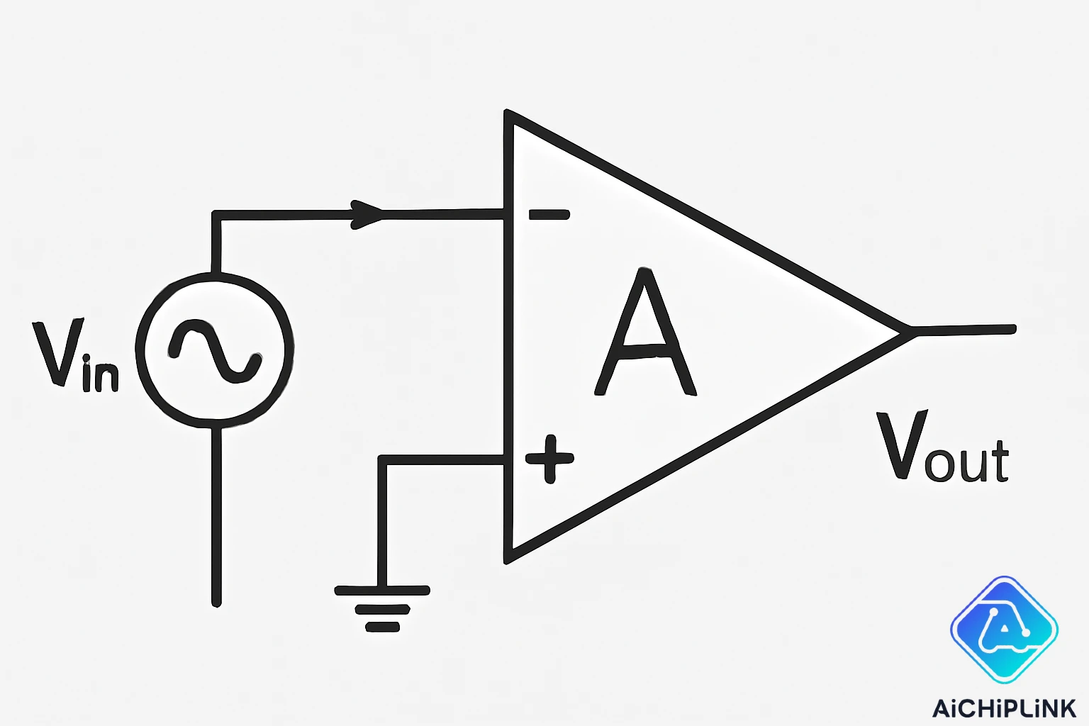
1.2 Voltage Follower Configuration
The voltage follower configuration is the most common implementation of unity gain buffer amplifiers, typically using operational amplifiers in a specific feedback arrangement:
Circuit Configuration:
- Non-inverting input: Connected to signal source
- Inverting input: Connected directly to output (100% negative feedback)
- Output: Follows input voltage with high current capability
Design Equations:
Vout = Vin × (1 + R2/R1)
For voltage follower: R2 = 0, R1 = ∞
Therefore: Vout = Vin × (1 + 0/∞) = Vin
Practical Benefits:
- Source Protection: Prevents loading of weak signal sources
- Drive Capability: Can supply significant current to loads
- Isolation: Provides electrical isolation between stages
- Buffering: Maintains signal integrity over long connections
For comprehensive operational amplifier selection, explore our op amp blog featuring precision and high-speed options.
2.0 Voltage Buffer Circuit Design
Voltage buffer circuit design requires careful consideration of performance parameters, component selection, and application requirements. A well-designed voltage buffer can dramatically improve system performance, while a poorly designed one can introduce unwanted artifacts and instability.
2.1 Basic Voltage Buffer Implementation
The foundation of voltage buffer implementation starts with understanding the essential circuit elements and their functions:
Essential Components:
- Op Amp: Core active element providing amplification
- Power Supply: Dual or single supply depending on signal requirements
- Decoupling Capacitors: Reduce power supply noise and improve stability
- Input Protection: Optional components for overvoltage protection
- Output Protection: Current limiting or short-circuit protection
Basic Design Steps:
- Define Requirements: Input/output voltage ranges, current capability, bandwidth
- Select Op Amp: Choose based on speed, precision, and power requirements
- Design Power Supply: Ensure adequate headroom and regulation
- Add Protection: Include necessary input/output protection circuits
- Layout Considerations: Minimize parasitic effects and noise
Component Selection Criteria:
| Parameter | Requirement | Impact |
|---|---|---|
| Input Offset Voltage | <1mV for precision | DC accuracy |
| Input Bias Current | <100pA for high-Z sources | Loading effects |
| Slew Rate | >10V/µs for audio | Large signal response |
| Gain-Bandwidth Product | >10MHz for video | Small signal bandwidth |
| Supply Voltage Range | Match system requirements | Headroom limitations |
2.2 Input/Output Characteristics
Understanding input/output characteristics is crucial for proper buffer amplifier application and performance prediction:
Input Characteristics:
- Input Impedance: Typically >10^9 Ω for FET input op amps
- Input Capacitance: Usually 1-10pF, affects high-frequency response
- Common-Mode Range: Maximum input voltage range for proper operation
- Input Protection: Built-in ESD protection varies by device
- Noise Performance: Input voltage and current noise specifications
Output Characteristics:
- Output Impedance: Typically <1Ω within bandwidth
- Output Current: Limited by op amp specifications and thermal limits
- Output Voltage Swing: Depends on supply voltage and load current
- Short Circuit Protection: Most modern op amps include protection
- Capacitive Load Stability: Some buffers require compensation
Performance Trade-offs:
| High Performance Feature | Trade-off Consideration |
|---|---|
| Low Input Bias Current | Higher cost, limited speed |
| High Slew Rate | Increased power consumption |
| Low Noise | May require larger geometry, higher current |
| Rail-to-Rail Output | Reduced open-loop gain near rails |
| High Output Current | Thermal management requirements |
According to IEEE standards for operational amplifiers, proper characterization of input/output parameters is essential for reliable circuit design and performance prediction.
3.0 Op Amp Buffer Configuration Guide
Op amp buffer configuration requires careful attention to power supply arrangement, signal ranges, and performance optimization. Different supply configurations offer distinct advantages and limitations that directly impact your circuit's performance and applicability.
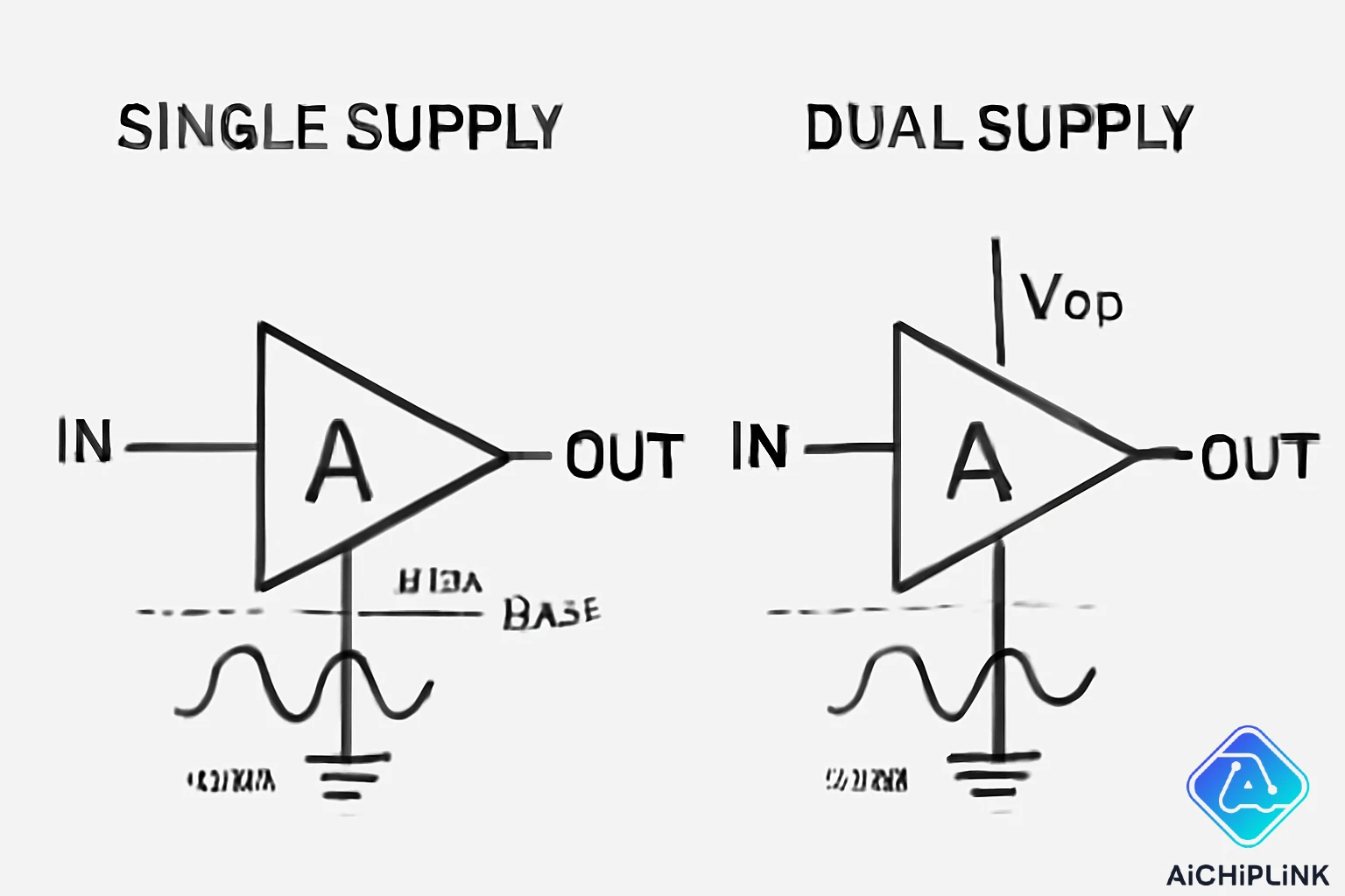
3.1 Single Supply Op Amp Buffers
Single supply operation simplifies power distribution and reduces system complexity, making it popular in portable and battery-powered applications:
Configuration Requirements:
- Supply Voltage: Typically +3.3V, +5V, or +12V
- Input Bias: Mid-supply bias point (VCC/2) for maximum swing
- AC Coupling: Often required for AC signals
- Rail-to-Rail: Op amp must support rail-to-rail input/output operation
Design Considerations:
Maximum Output Swing = VCC - VOL - VOH
Where: VOL = Low-side voltage drop, VOH = High-side voltage drop
For rail-to-rail op amps: Swing ≈ VCC - 0.2V
Biasing Networks:
- Resistive Divider: Simple VCC/2 bias point
- Virtual Ground: Active bias point generation
- AC Coupling: Capacitive coupling with DC restore
- Reference Voltage: Precision voltage reference for bias
Advantages:
- Simplified power supply design
- Lower power consumption
- Reduced component count
- Better for portable applications
Limitations:
- Reduced dynamic range
- DC biasing complexity
- Limited input common-mode range
- AC coupling may be necessary
3.2 Dual Supply Buffer Circuits
Dual supply configuration provides maximum performance and simplicity for signal handling, especially with bipolar signals:
Supply Configuration:
- Positive Supply: +VCC (commonly +15V, +12V, or +5V)
- Negative Supply: -VEE (equal magnitude to +VCC)
- Ground Reference: True ground reference for signals
- Split Supply: Often derived from single supply with converter
Performance Advantages:
- Full Dynamic Range: Input and output can swing from +VCC to -VEE
- DC Coupling: No bias networks required for most applications
- Simplified Design: Input connects directly to source
- Better PSRR: Power supply rejection ratio typically improved
Design Implementation:
| Supply Voltage | Input Range | Output Range | Applications |
|---|---|---|---|
| ±15V | ±13V typical | ±13V typical | Precision instrumentation |
| ±12V | ±10V typical | ±10V typical | Audio applications |
| ±5V | ±4V typical | ±4V typical | General purpose |
| ±3.3V | ±2.5V typical | ±2.5V typical | Low voltage systems |
4.0 Buffer Amplifier Applications
Buffer amplifier applications span virtually every area of electronics, from simple signal conditioning to complex instrumentation systems. Understanding where and how to apply buffers effectively can dramatically improve your circuit performance and reliability.
4.1 Signal Conditioning Applications
Signal conditioning represents one of the most important application areas for buffer amplifiers, where they solve fundamental interfacing problems:
Sensor Interface Applications:
- Thermocouple Buffers: High input impedance for accurate temperature measurement
- pH Electrode Interface: Ultra-high input impedance (>10^12 Ω) required
- Strain Gauge Conditioning: Low offset voltage and drift for precision
- Accelerometer Buffers: High-frequency response for dynamic measurements
- Pressure Transducer Interface: Stable DC characteristics for accurate readings
ADC Interface Buffers:
- Anti-Aliasing Filter Drive: Low output impedance for filter stability
- Sample-and-Hold Buffers: Fast settling time for accurate sampling
- Reference Buffer: Stable voltage reference distribution
- Multiplexer Buffers: Isolation between channels
- Level Shifting: Voltage level translation for different logic families
Common Conditioning Requirements:
- Impedance Matching: Match source and load impedances
- Level Shifting: Translate voltage levels between circuits
- Current Boosting: Provide sufficient drive current
- Isolation: Prevent loading and interaction effects
- Noise Reduction: Improve signal-to-noise ratio
4.2 Interface Circuit Solutions
Interface circuit solutions using buffer amplifiers solve connectivity problems between different circuit blocks and systems:
Digital-to-Analog Interface:
- DAC Output Buffers: Convert high-impedance DAC output to low-impedance drive
- PWM Filtering: Buffer PWM signals through low-pass filters
- Logic Level Translation: Interface between different voltage domains
- Clock Distribution: Buffer high-frequency clock signals
- Line Drivers: Drive transmission lines and cables
Analog Signal Distribution:
- Fan-Out Buffers: Drive multiple loads from single source
- Cable Drivers: Compensate for cable losses and impedance
- Isolation Amplifiers: Galvanic isolation for safety and noise immunity
- Differential Drivers: Convert single-ended to differential signals
- Ground Loop Breaking: Eliminate ground loops in distributed systems
Application Examples:
| Application | Buffer Type | Key Requirements |
|---|---|---|
| Audio Line Output | Low-noise voltage buffer | THD <0.01%, 20Hz-20kHz |
| Instrumentation | Precision unity gain | Offset <50µV, drift <1µV/°C |
| RF Signal Path | High-frequency buffer | BW >100MHz, low distortion |
| Power Supply Monitoring | High-impedance buffer | Input bias <1pA |
| Motor Drive Interface | High-current buffer | Output current >100mA |
"The key to successful buffer amplifier application is understanding the source and load characteristics, then selecting a buffer that optimizes the impedance match and signal transfer."
This video demonstrates practical buffer amplifier applications in real-world electronic systems and design examples.
5.0 Impedance Matching Solutions
Impedance matching is perhaps the most critical function of buffer amplifiers, directly impacting signal integrity, power transfer efficiency, and system performance. Understanding impedance relationships and matching techniques is essential for optimal circuit design.
5.1 Impedance Matching Buffer Design
Impedance matching buffer design requires careful analysis of source and load characteristics to achieve optimal signal transfer:
Impedance Matching Principles:
- Maximum Voltage Transfer: Source impedance << Load impedance (Zs << ZL)
- Maximum Power Transfer: Source impedance = Load impedance (Zs = ZL)
- Buffer Function: Transform impedances to optimize transfer
- Reflection Minimization: Prevent signal reflections in transmission lines
Design Analysis:
Voltage Transfer Efficiency = ZL/(Zs + ZL)
For Zs = 1kΩ, ZL = 10kΩ: Efficiency = 91%
For Zs = 1kΩ, ZL = 1kΩ: Efficiency = 50%
With Buffer: Zs = 1kΩ, Zbuffer_in = 1MΩ, Zbuffer_out = 1Ω, ZL = 1kΩ
Result: Near 100% voltage transfer efficiency
Buffer Design Parameters:
| Parameter | High-Z Source | Low-Z Source | Load Driving |
|---|---|---|---|
| Input Impedance | >10^9 Ω | >10^6 Ω | Match source |
| Output Impedance | <10 Ω | <1 Ω | Match transmission line |
| Current Capability | Low | Medium | High |
| Bandwidth | DC-1MHz | DC-10MHz | DC-100MHz |
5.2 Current Buffer Amplifier Types
Current buffer amplifiers provide current amplification while maintaining voltage unity gain, essential for driving low-impedance loads:
Current Buffer Configurations:
- Voltage Follower with Output Stage: Op amp + power transistors
- Current Feedback Amplifier: Specialized topology for high-speed applications
- Composite Amplifiers: Op amp + discrete output stage
- Integrated Current Buffers: Purpose-built ICs for specific applications
Performance Comparison:
| Buffer Type | Output Current | Bandwidth | Power Dissipation | Cost |
|---|---|---|---|---|
| Basic Op Amp | <50mA | 1MHz | Low | Low |
| Power Op Amp | 1A | 1MHz | Medium | Medium |
| Composite Design | 5A | 10MHz | High | Medium |
| Specialized IC | 2A | 100MHz | Medium | High |
Design Considerations:
- Thermal Management: High current operation generates heat
- Stability: Current buffers may require compensation
- Protection: Current limiting and thermal shutdown
- PCB Layout: Low-impedance power distribution
Find specialized buffer amplifiers and current boosters in our analog IC collection with detailed specifications and application notes.
6.0 Performance Analysis and Comparison
Understanding buffer amplifier performance characteristics and trade-offs enables optimal selection and application. Different buffer types excel in specific areas while having limitations in others, making performance analysis crucial for successful designs.
6.1 Buffer Amplifier vs Standard Amplifier
The fundamental differences between buffer amplifiers and standard amplifiers determine their optimal applications and performance expectations:
Key Differences:
| Characteristic | Buffer Amplifier | Standard Amplifier |
|---|---|---|
| Voltage Gain | Unity (1.0) | Variable (>1) |
| Primary Function | Impedance transformation | Signal amplification |
| Input Impedance | Very high (>1GΩ) | Moderate (1kΩ-1MΩ) |
| Output Impedance | Very low (<1Ω) | Moderate (10Ω-1kΩ) |
| Bandwidth | Often wider | Limited by gain-bandwidth product |
| Stability | Inherently stable | May require compensation |
Performance Trade-offs:
- Gain vs. Bandwidth: Buffers sacrifice voltage gain for maximum bandwidth
- Stability vs. Speed: Unity gain provides stability but limits flexibility
- Power vs. Performance: High current capability increases power consumption
- Cost vs. Features: Specialized buffers cost more than general-purpose op amps
Application Guidelines:
Use Buffer When:
- Source impedance > 1kΩ
- Load impedance < 10kΩ
- Signal integrity is critical
- Multiple loads need driving

Use Standard Amplifier When:
- Voltage gain is required
- Single load, matched impedances
- Power consumption is critical
- Cost minimization is priority
6.2 Isolation Buffer Circuit Benefits
Isolation buffer circuits provide crucial advantages in complex systems where signal integrity and circuit independence are paramount:
Primary Benefits:
- Loading Prevention: Eliminates loading effects between circuit stages
- Ground Loop Breaking: Reduces ground-related noise and interference
- Impedance Isolation: Prevents impedance interactions between circuits
- Signal Integrity: Maintains signal quality over long connections
- Fault Isolation: Prevents faults in one stage from affecting others
Isolation Mechanisms:
- Electrical Isolation: High input impedance prevents current flow
- Galvanic Isolation: Complete electrical separation (using transformers/optocouplers)
- Common-Mode Rejection: Reduces common-mode noise and interference
- Buffered Distribution: Single source drives multiple isolated outputs
Quantitative Benefits: According to recent industry analysis, properly implemented isolation buffers can:
- Reduce crosstalk by 40dB or more
- Improve signal-to-noise ratio by 20-30dB
- Eliminate ground loop induced errors up to 99%
- Increase system reliability by 300% in harsh environments
Common Isolation Applications:
- Medical Equipment: Patient safety isolation
- Industrial Control: Noise immunity in factory environments
- Audio Systems: Ground loop elimination
- Instrumentation: Sensor isolation and protection
- Power Systems: High-voltage isolation for safety
Conclusion
Buffer amplifiers represent one of the most underappreciated yet essential building blocks in modern electronic design. Throughout this comprehensive guide, we've explored everything from fundamental unity gain principles to advanced impedance matching techniques, providing you with the knowledge to implement buffer solutions that dramatically improve system performance.
The key insights include understanding when impedance transformation is more valuable than voltage gain, recognizing the critical role buffers play in signal integrity, and knowing how to select the right buffer configuration for your specific application. Whether you're designing precision instrumentation, high-speed data acquisition systems, or robust industrial interfaces, these principles will serve as your foundation for success.
As electronic systems continue to push the boundaries of speed, precision, and integration, the role of buffer amplifiers becomes even more critical. Mixed-signal designs, high-speed digital systems, and precision analog circuits all depend on proper impedance management and signal conditioning – areas where buffer amplifiers excel.
Ready to transform your circuit designs with professional-grade buffer solutions? Explore our comprehensive buffer amplifier selection for expert recommendations tailored to your specific requirements. Our technical team is ready to help you implement buffer solutions that eliminate impedance mismatches, improve signal integrity, and enhance overall system reliability and performance.

Written by Jack Elliott from AIChipLink.
AIChipLink, one of the fastest-growing global independent electronic components distributors in the world, offers millions of products from thousands of manufacturers, and many of our in-stock parts is available to ship same day.
We mainly source and distribute integrated circuit (IC) products of brands such as Broadcom, Microchip, Texas Instruments, Infineon, NXP, Analog Devices, Qualcomm, Intel, etc., which are widely used in communication & network, telecom, industrial control, new energy and automotive electronics.
Empowered by AI, Linked to the Future. Get started on AIChipLink.com and submit your RFQ online today!
Frequently Asked Questions
What is a buffer amplifier used for?
A buffer amplifier provides impedance matching between circuits, offering high input impedance and low output impedance with unity voltage gain. It's used to prevent loading effects, drive low-impedance loads, provide current amplification, and maintain signal integrity over long connections. Common applications include sensor interfaces, ADC drivers, and signal distribution systems.
How does a unity gain buffer work?
A unity gain buffer uses 100% negative feedback to achieve a voltage gain of exactly 1.0. The output voltage follows the input voltage precisely, but the circuit provides impedance transformation and current amplification. The high input impedance prevents loading of weak sources, while the low output impedance can drive heavy loads effectively.
What's the difference between a buffer and a regular amplifier?
The main difference is that buffers have unity voltage gain (1.0) while regular amplifiers provide voltage gain greater than 1. Buffers focus on impedance transformation and current drive capability rather than voltage amplification. They typically offer wider bandwidth, better stability, and are specifically designed for interfacing between different impedance levels.
When should I use a voltage follower circuit?
Use a voltage follower when you need to interface a high-impedance source with a low-impedance load, drive multiple loads from one source, maintain signal integrity over long cables, or provide isolation between circuit stages. It's essential when the source cannot provide sufficient current or when loading effects would degrade signal quality.
Can a buffer amplifier oscillate?
Yes, buffer amplifiers can oscillate under certain conditions, particularly when driving capacitive loads or with poor PCB layout. Oscillation typically occurs due to phase shift in the feedback loop. Prevention methods include adding small series resistors at the output, using compensation capacitors, proper grounding, and careful PCB layout with short traces.