Synchronous Rectification Guide: How It Works, MOSFET Selection and Applications
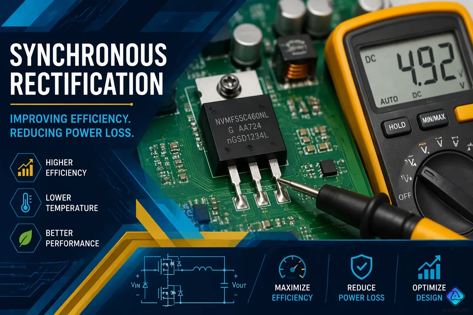
Synchronous rectification uses a controlled MOSFET instead of a rectifier diode. This switch lets current flow with much lower voltage drop and heat than a diode. That difference creates real gains in efficiency.
You will find synchronous rectification in most modern dc-dc converters. It is a core power electronics technique. The control circuit can also manage current direction, so power flows where the design needs it. Lower loss also means a simpler thermal design. A diode always drops a fixed forward voltage. A MOSFET acts like a small resistor instead.
This synchronous rectification guide covers the working principle, MOSFET selection, solution types, and applications.
Key Takeaways
-
Synchronous rectification uses a MOSFET instead of a diode to lower voltage drop and heat.
-
Pick a MOSFET with low on-resistance, and check it at the gate voltage and temperature you actually use.
-
Set the dead time carefully to prevent shoot-through and body diode losses.
-
Use synchronous rectification in low-voltage, high-current designs to improve efficiency.
-
Turn off synchronous rectification during startup when the load is pre-biased, so it does not fail.
Synchronous Rectification Guide: The Basics
Definition and Core Benefit
Synchronous rectification replaces a rectifier diode with a controlled MOSFET. The MOSFET switches on whenever the diode would normally let current through. This one change lowers both voltage drop and heat at the same time. The rectifier stage then acts like a very small resistor instead of a fixed voltage barrier. A driver circuit controls when the device turns on and off, so you stay in charge of the timing.
This synchronous rectification guide treats the technique as a basic building block of modern power electronics. You will find it inside most dc-dc converters today. The control circuit also sets which way current flows. A synchronous rectifier can block reverse flow or allow it on purpose. That direction control is the second benefit, right after higher efficiency. This approach really pays off when every watt counts.
Why Conduction Loss Drops
A diode keeps a fixed forward drop, usually 0.7 V to 1.4 V per device. A MOSFET conducts through its on-resistance instead, and high-performance parts often stay below 10 mΩ. Synchronous rectification swaps that fixed drop for a resistive channel. The table below shows how the two compare.
| Aspect | Rectifier Diode | MOSFET (Synchronous Rectification) |
|---|---|---|
| Voltage drop | Fixed forward drop | Very small resistive drop |
| Loss scaling | Loss ≈ V_f × I | Loss ≈ I²R |
| Typical efficiency | Bridge rectifiers 85–95% | Above 98% |
| Heat | Higher | Lower |
Diode conduction losses go up in a straight line as current rises. MOSFET conduction loss grows with the square of current, but a tiny resistance keeps the actual value low. That is why conduction losses drop so sharply in low-voltage, high-current designs. Compare parts at the current your design really delivers, not at a headline rating. Small resistance values also mean less heat to remove from the board. The same reasoning explains why this synchronous rectification guide puts on-resistance above almost every other parameter. A well-chosen synchronous rectifier can push efficiency past 98%, while a diode bridge usually stays in the 85–95% range.
How Synchronous Rectification Works
A synchronous rectifier replaces the diode with a controlled MOSFET and driver logic. The device conducts in place of the diode, and the control circuit decides when it turns on and off. N-channel parts are used most in these designs for good reason. Their low on-resistance keeps the forward drop small, and that is the whole point of the technique.
| Attribute | N-channel MOSFET | P-channel MOSFET |
|---|---|---|
| Carrier mobility in silicon | ~1,400 cm²/(V·s) | ~450 cm²/(V·s) |
| RDS(on) per die area | Lower | Higher |
| Die size for equal RDS(on) | Baseline | 2–3× larger |
| Relative cost for same RDS(on) | Lower | Higher |
Electrons move about three times faster than holes in silicon. So an N-channel part needs less die area for the same on-resistance. In high-efficiency power supplies, N-channel MOSFETs replace Schottky diodes. This cuts the forward drop from roughly 0.5 V to below 0.1 V. That change sharply reduces conduction losses and improves thermal performance. This is why synchronous rectification sits at the center of modern power electronics.
Above 10 A, an N-channel MOSFET is basically required to avoid thermal runaway; P-channel devices are only the smarter choice in sub-2 A designs where PCB space is the main limit.
Non-Isolated Topologies
Synchronous rectification in this stage is the simplest case to study. The synchronous buck converter is the classic case. The high-side MOSFET chops the input, and the low-side synchronous MOSFET replaces the catch diode. Both devices switch in alternation, and dead time prevents shoot-through. Gate drivers control the pair with tight timing, and that timing sets the efficiency you actually get. Current direction control matters here too. You can monitor current and disable the switch below a set threshold, or detect reverse flow and stop operation. A comparator sensing negative current gives a simple yes/no signal to the controller or the FET driver. Keep that sensing path short and clean, or the comparator will trip on noise. Two devices back-to-back provide bidirectional blocking at the cost of higher drop and gate capacitance. Watch the parasitic body diode, which conducts in reverse and can weaken your direction control. A second synchronous buck converter stage, such as a multiphase rail, follows the same rules.
Isolated Topologies
Isolated designs mirror the same behavior, with a transformer adding isolation. The secondary-side synchronous rectifier acts like diode commutation of the transformer's AC.
-
At the start of conduction, current flows through the body diode of the power MOSFET and creates a negative drain-to-source voltage larger than the channel drop.
-
When that voltage crosses the turn-on threshold, the logic drives the gate on and
VDSfalls. -
The control logic must react fast, because the body diode conducts until the gate turns on.
-
The device stays on until the rectified current decays and
VDScrosses the turn-off threshold.
A pair of comparators can differentially sense VDS to judge current polarity and switch near zero-current transitions. Here dead time and gate drivers matter just as much as in a non-isolated stage.
The flyback topology is basically the buck-boost topology isolated by a transformer acting as the storage inductor, while the forward converter is basically a transformer-isolated buck converter.
That framing explains why synchronous rectifiers in isolated topologies mirror their non-isolated counterparts. Synchronous rectification works the same way in both families.
MOSFET Selection for Synchronous Rectification
Good mosfet selection starts with five parameters. You must weigh drain-source voltage, continuous drain current, on-resistance, gate voltage, and switching speed together. No single number decides the part.
Key Parameters for Synchronous Rectifier MOSFETs
The table below sums up what each parameter asks of your design.
| Parameter | Key Selection Consideration |
|---|---|
| VDS | Must handle normal input plus overshoot, ringing, and spikes. Never let the highest expected circuit voltage go past 80% of rated VDS. A 24 V system with 32 V spikes needs a 60 V or 80 V device. |
| ID | A theoretical maximum under perfect thermal conditions. Real current depends on package thermal resistance, copper area, airflow, and on-resistance at operating temperature. Treat ID as a qualification parameter. |
| RDS(on) | Set it from your conduction-loss budget: mosfet conduction loss = I² × RDS(on). Check the value at your real gate voltage and at top temperature. |
| Gate voltage | Confirm the real drive voltage and check on-resistance at that VGS. For 3.3 V or 5 V MCU drive, use a logic-level mosfet rated at low VGS. |
| Switching speed | Qg sets gate-drive loss (Qg × VGS × fSW). Qgd sets transition time. Above 500 kHz, put low Qg, Qgd, and Coss ahead of the lowest on-resistance. |
A low on-resistance part often comes with a big die, high Qg, and high Coss. At high frequency, those switching losses can be bigger than the conduction savings. The comparison below shows the trade-off.
| Parameter | MOSFET A | MOSFET B |
|---|---|---|
| VDS | 80 V | 80 V |
| RDS(on) | 3 mΩ | 7 mΩ |
| Qg | 180 nC | 50 nC |
| Gate-drive loss at 10 V, 500 kHz | ≈ 0.9 W | ≈ 0.25 W |

MOSFET A wins on conduction losses. MOSFET B runs cooler at 500 kHz. The best part depends on your operating point and topology.
Watch the body diode too. Its forward voltage drives dead time loss, and a low reverse recovery charge matters at high frequency. Capacitance values change in a nonlinear way against VDS, so charge-based figures give more reliable energy estimates.
Ratings, Protection, and Power MOSFETs
The breakdown rating must survive the flyback voltage, which can run far above the battery voltage. Work out the stress from output voltage, maximum input voltage, and maximum duty cycle. Then add a safety margin. Modern power mosfets with built-in temperature, current, and voltage protection make this task easier. Optimization charts for the latest generations of power mosfets let you compare on-resistance against gate charge at a glance. Use them during selection to make a short list of candidates fast. These power mosfets also work well with smart gate drivers that handle fault reporting. In power electronics, that combination shortens design cycles.
Types of Synchronous Rectification Solutions
Controller-Driven and Self-Driven
A controller-driven synchronous rectifier uses a special IC to decide when the MOSFET turns on and off. The IC checks the drain-to-source voltage of the MOSFET or the current in the channel, then tells the gate what to do. This gives you tight control over timing, and it works with many topologies. Dedicated gate drivers sit between the IC and the MOSFET, so the turn-on edge stays sharp and switching loss stays low. You also get fault reporting and clean shutdown from the controller.
Self-driven designs get the gate signal from the transformer winding or the main switch node. You save the cost of a controller, and the timing follows the power stage on its own. The trade-off is less freedom to tune timing, so the winding voltage must fit the gate of the MOSFET. Check that the drive stays inside the gate rating of the MOSFET at every input voltage. A small clamp circuit protects the gate when the winding voltage runs high.
Integrated and Discrete Options
You can build the stage from an integrated solution or from discrete parts. Integrated synchronous rectification puts the switch and control logic into one package. Discrete designs pair a controller with separate power mosfets. Both routes show up across power electronics, and each one fits a different set of goals.
| Aspect | Integrated | Discrete |
|---|---|---|
| Efficiency | Fast switching, low body-diode stored charge | Slower body-diode reverse recovery |
| Switching frequency | Above 1 MHz, dead times under 20 ns | Around 300 kHz, dead times near 60 ns |
| EMI | Lower, no snubber needed | Larger traces raise parasitics |
| Thermal design | Tab at ground potential | Tab at drain potential |
| MOSFET choice | Limited RDS(on) range | Wide RDS(on) range |
Integrated parts make layout and thermal design simpler. Discrete parts let you tailor the MOSFET to your output current. Many designers pair a small IC with several PWM controllers to balance cost and performance. Choose discrete power mosfets when you need a wide RDS(on) range. Choose an integrated synchronous rectifier when board space and EMI matter most. Either way, match the gate drivers to the MOSFET you pick. Weigh the die size and package cost of a fully integrated part against the flexibility of a discrete layout.
Synchronous Rectification vs. Schottky Diodes
Efficiency and Loss Trade-Offs
A Schottky diode always drops the same forward voltage, so it turns power into heat every time current flows through it. That drop is usually 0.4–0.7 V, and it wastes a share of system power as conduction loss. The waste hurts most at low output voltage and high current, where the drop takes a big share of the rail.
The secondary-side diode rectification structure does not give enough efficiency because of forward voltage drop losses (0.4–0.7 V). This causes a lot of power dissipation and limits USB-PD flyback converter performance. Adding synchronous rectification requires precise timing control.
A synchronous rectifier replaces that fixed drop with a low on-resistance channel, so mosfet conduction loss stays far below the diode loss. The gain is real, but there is a catch. The body diode still conducts until the gate turns on, and it drops 0.6–1 V during that time. Bad turn-off timing makes things worse. Turning off too early forces body diode conduction with reverse recovery losses. Turning off too late allows reverse current and shoot-through. You trade lower conduction losses for sensitivity to timing precision.
Cost, Complexity, and Fit
A Schottky diode rectifies by itself. It needs no drive circuit, no timing logic, and no dead-time control. That simplicity keeps cost down and appeals to designs where reliability matters more than peak efficiency. Diodes also hold an edge at light load, where their behavior stays predictable.
Synchronous rectification adds a mosfet, a driver, and control logic. The extra circuitry raises cost and design effort, and it can make reliability seem lower. The mosfet also switches fast, which can raise EMI and demand careful layout. Still, the payoff is large at high current and low duty cycle. Pick the synchronous rectifier when efficiency targets are tight. Pick the diode when cost, simplicity, and stability lead your list. In power electronics, both paths remain valid, and the right fit depends on your load profile and budget.
Common Applications and Use Cases
Consumer and Computing Power
Consumer devices rely on synchronous rectification whenever a battery or adapter powers a low-voltage rail at high current. Phone chargers and USB-PD adapters use it on the secondary side of the flyback stage. This technique lowers the fixed diode drop and pushes efficiency past 98% in well-tuned designs. Laptops, tablets, and desktop motherboards use it in the synchronous buck converter that feeds the processor core. Those rails need tight regulation at currents that would overheat a Schottky diode.
You will also find it inside very low-voltage, high-current power rails on graphics cards and servers. A mosfet with on-resistance below 10 mΩ keeps the conduction loss small at these current levels. The mosfet also lets the controller block reverse current when a rail shuts down. Designers of low-voltage, high-current switching converters treat this stage as standard practice today. Every millivolt saved at the load means longer battery life or a smaller thermal solution.
Industrial and Automotive Power
Industrial systems use synchronous rectification in motor drives, PLC supplies, and battery-backed equipment. A 48 V bus often feeds point-of-load converters through a synchronous buck converter stage. The mosfet handles high current with modest heat, so cabinets need less forced air. Tough environments also benefit from the lower dissipation, because sealed enclosures leave little room for cooling.
Automotive designs apply the technique in DC-DC modules, onboard chargers, and LED drivers. Alternator and battery voltages swing widely, so the mosfet must survive flyback spikes well above the nominal rail. Engineers in power electronics pair protected power mosfets with smart gate drivers for this reason. Start-stop systems and mild hybrids add another layer of demand. These power converters must stay efficient across a wide input range, and a well-chosen mosfet keeps losses low at every operating point. The same efficiency gain that helps a phone charger also helps a traction auxiliary supply.
Choosing an SR Solution Step by Step
Define Requirements and Shortlist
Begin your synchronous rectification selection with the basics. First, narrow the candidates by voltage rating, package, and on-resistance. Then match the topology to the critical specs. For a synchronous rectifier or bridge, the key parameters are reverse recovery charge and gate timing. Body-diode recovery and shoot-through decide whether the stage runs cool or overheats.
Compare reverse recovery charge at matching conditions. Datasheet values come from fixed JEDEC conditions and include part of the output charge. The effective value depends on how long the body diode conducts before turn-off. So check it at your circuit's real conditions. Next, check the gate-driver interface. Compare threshold voltage and gate charge against your existing gate drivers. A higher threshold may not fully turn on from a logic-level drive. A much higher gate charge slows switching or overloads the driver and risks shoot-through. Verify the safe operating area at your pulse width and temperature wherever the mosfet works in the linear region or handles inrush. Compare the avalanche rating by method and conditions against the inductive-switching energy where no clamp path exists. These steps only screen candidates. Final validation requires testing the exact part in your circuit.
Validate and Prototype
Begin with simulations to get an early look at the switching patterns of a full-bridge converter with synchronous rectification. Build the first prototype with the selected topology, then validate it to confirm your design decisions. Validate the switching patterns of all main switches, including the SR switches, before you continue. This step is required for digitally controlled converters. A full-bridge converter has complex switching states, so use an 8-channel oscilloscope to capture all relevant signals at once. Set a sampling rate of at least 1 Gsample and a sufficient record length. Verify the measured pattern against theory. In one example (100 W isolated DC/DC, 48 V to 12 V at up to 8 A, ~100 kHz), the waveforms matched and passed. Check the minimum dead time between synchronous switch turn-off and primary leg turn-on to prevent shoot-through. Measured values were 264 ns and 328 ns.
| Test Category | Requirement |
|---|---|
| Temperature cycling | 500–1000 cycles from -40°C to 125°C without degradation |
| Automotive qualification | AEC-Q101 compliance |
| Shoot-through fault testing | dV/dt of 5–50 V/ns to verify parasitic turn-on immunity |
| Surge immunity | IEC 61000-4-5, 1–2 kV without permanent damage |
| Accelerated life testing | 1000 hours at 125°C and 120% rated voltage |
| Humidity bias | 85°C/85% RH for 1000 hours |
Manage junction temperature as the main thermal parameter. Most SR mosfets are rated for 150–175°C maximum, so you need a good thermal path from junction to ambient. Use copper pour areas, thermal vias, and wider high-current traces to spread heat. Run thermal simulation during development to find hotspots before prototyping.
Common Mistakes and Troubleshooting
Most synchronous rectifier problems come from timing or layout. A careful look at common mistakes, problems, and troubleshooting in synchronous rectification saves you prototype cycles and protects your efficiency target.
Timing and Dead-Time Issues
The synchronous rectifier must turn off before its current reverses. Positive current must still flow through the mosfet channel at turn-off. The current then moves into the body diode. A long off delay lets the mosfet conduct after reversal, and body-diode conduction plus surge behavior follows. Tune primary dead time and secondary off delay separately, because no direct link joins them.
-
Set the SR off delay at 50% of the DELAB setting (DELAB = 200 ns gives 100 ns).
-
Repeat the test using the DELAB measured at 100% load.
-
Check dead time across the load range, since primary dead time falls with load while secondary off delay rises.
Check each dead time value on the bench. A dead time that works at light load can fail at full load. Watch the mosfet body diode during every dead time window. A mosfet that turns on too early creates shoot-through, and a mosfet that turns off too late wastes the dead time gain. Keep the dead time short but safe.
Layout and Thermal Pitfalls
Keep the source of the synchronous rectifier mosfet short to GND. Keep the gate trace short to the SR pins. Long loops pick up noise, and your gate drivers then switch the mosfet at the wrong moment. Think about continuous conduction mode (CCM) when you pick a synchronous rectification part, because the mosfet conducts longer there and timing errors cost efficiency.
| Category | Pitfall | Consequence |
|---|---|---|
| Layout | Asymmetrical traces between parallel mosfet | Imbalanced current sharing |
| Layout | Unequal thermal vias | Temperature gradients |
| Thermal | Reliance on RDS(on) self-balancing | Insufficient balancing |
| Thermal | No temperature monitoring | Thermal runaway risk |
Match gate drivers and thermal paths across parallel mosfet. Add sensors and derating to prevent synchronous rectifier problems in the field. A mosfet with a poor thermal path runs hot, and heat shifts its dead time behavior. These steps cover the common mistakes, problems, and troubleshooting cases you will meet.
When to Use or Avoid Synchronous Rectification
Best-Fit Scenarios
You get the most from synchronous rectification when the output rail is low and the current is high. A fixed diode drop takes a big share of a low rail. A mosfet channel does not. The numbers make the case clearly.
| Scenario | Rectifier type | Power loss | Notes |
|---|---|---|---|
| 24V → 5V/2.5A DC-DC | Diode | 0.99 W | Baseline |
| 24V → 5V/2.5A DC-DC | Synchronous rectifier | 0.40 W | Losses more than halved; ~30°C lower temperature rise; smaller solution possible for same rise |
The gain grows as the output voltage falls. That is why low-voltage, high-current converters almost always use it. Regulation also gets better. A synchronous mosfet conducts in both directions, so the converter stays in continuous conduction mode at light load. Your loop keeps the duty-cycle relationship it was tuned for. If light-load efficiency is your main goal, turn off the rectifier or use a pulse-skipping mode instead.
One startup case needs care. In systems with sequenced rails, the converter may start into a pre-biased load.
Because a synchronous rectifier mosfet conducts in both directions, current can flow back into the converter during soft-start, and this may stop it from starting up properly. Disable synchronous rectification during startup and let the body diode free-wheel; the extra dissipation is insignificant.
Boost and buck-boost stages make synchronous rectification less straightforward, since the mosfet lacks a ground-referenced drive. The issue matters little there, because those topologies deliver higher outputs.
Cases Where Diodes Fit Better
A diode bridge still wins on a high-voltage DC bus. The fixed drop is a small fraction of the output, so simplicity and robustness carry more weight. Diodes also suit designs where shoot-through risk and dead time tuning feel like unnecessary burdens. A diode needs no gate drivers and no timing logic. It simply rectifies.
Weigh both paths against your real operating point before you decide when to use synchronous rectification. Match the choice to your voltage, current, and cost targets.
Synchronous rectification cuts voltage drop and heat. It boosts efficiency in dc-dc converters and battery devices. A mosfet conducts through RDS(on), so a low-resistance part wastes little power. This synchronous rectification guide shows the technique works with many topologies.
Check VDS, ID, RDS(on), gate voltage, and switching speed for every mosfet on your list. Plan the thermal path and control timing, including dead time, early. Tune dead time across the load range, and make sure each mosfet stays cool.
Use this synchronous rectification guide to match the approach to your voltage, current, and cost targets. Don't just use it by default. Expect the mosfet to keep making higher-efficiency designs possible. New mosfet generations will keep pushing losses down.

Written by Jack Elliott from AIChipLink.
AIChipLink, one of the fastest-growing global independent electronic components distributors in the world, offers millions of products from thousands of manufacturers, and many of our in-stock parts is available to ship same day.
We mainly source and distribute integrated circuit (IC) products of brands such as Broadcom, Microchip, Texas Instruments, Infineon, NXP, Analog Devices, Qualcomm, Intel, etc., which are widely used in communication & network, telecom, industrial control, new energy and automotive electronics.
Empowered by AI, Linked to the Future. Get started on AIChipLink and submit your RFQ online today!
Frequently Asked Questions
What is synchronous rectification in simple terms?
It swaps a rectifier diode for a controlled MOSFET that turns on whenever the diode would conduct. The switch behaves like a tiny resistor instead of a fixed voltage barrier. You get less voltage drop and less heat, and the controller can also steer current direction.
Why does a mosfet beat a Schottky diode on loss?
A Schottky diode drops 0.4–0.7 V every time current flows. A mosfet channel drops far less at high current. That gap drives the efficiency gain, which often pushes well-tuned designs past 98%. The trade-off is timing: the body diode conducts until the gate turns on.
How do I pick a mosfet for an SR stage?
Screen candidates on five numbers: VDS, ID, RDS(on), gate voltage, and switching speed. Keep the highest expected voltage below 80% of rated VDS, then add margin for spikes. Check RDS(on) at your real gate drive and at top temperature. A low-resistance mosfet with high Qg can lose at high frequency.
What causes SR timing failures?
Dead time sits at the root of most failures. Turn the mosfet off too early and the body diode carries current with reverse recovery loss. Turn it off too late and reverse current flows. Tune primary dead time and secondary off delay separately, and check both across the full load range.
Can I use synchronous rectification in every design?
No. It fits low-voltage, high-current rails best, where a fixed diode drop eats a large share of the output. High-voltage buses and cost-sensitive, low-complexity designs often suit a diode better. Disable the mosfet during soft-start into a pre-biased load, or startup may fail.