Silicon Carbide (SiC) Guide: The Third-Generation Semiconductor Material for Modern Electronics
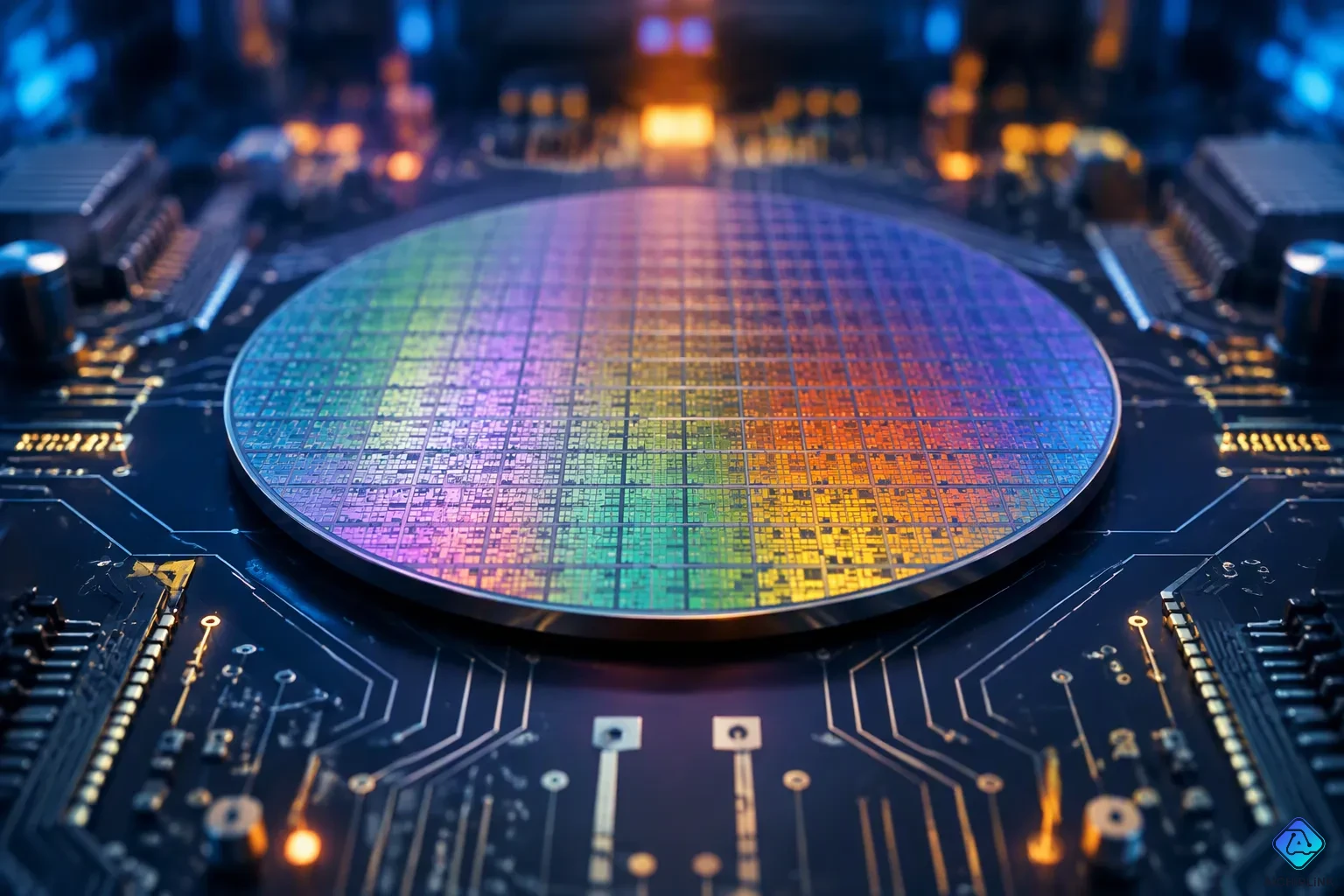
Silicon carbide (SiC) is a third-generation semiconductor material. It joins silicon and carbon atoms in a crystal with a wide bandgap. This compound gives high breakdown voltage, great thermal conductivity, and better efficiency. These traits help SiC beat silicon's limits in high-power and high-temperature settings. The silicon carbide market grows fast, with a 23.8% CAGR from 2022 to 2030. SiC devices boost energy efficiency by 10% in EV inverters. SiC-based solar inverters reach 99% efficiency. This guide also covers what SiC is, its key advantages over silicon, its main uses in power electronics and modern tech, and where the technology is going.
Key Takeaways
-
Silicon carbide (SiC) is a third-generation semiconductor material. It can handle higher voltage, temperature, and frequency than silicon.
-
SiC devices cut energy losses by up to 41% in power systems. This helps electric vehicles go farther and charge faster.
-
SiC increases solar inverter efficiency to 97.5% and helps 5G networks work better.
-
The SiC market is growing quickly, at more than 23% each year. Costs go down when wafer sizes get bigger, from 150 mm to 200 mm.
-
Making things with SiC is still hard. Flaws and low output are common problems. But scientists keep studying it. Their work will help SiC reach its full power.
What Is Silicon Carbide (SiC)?
Silicon carbide (SiC) is a compound semiconductor. It is made of silicon and carbon atoms in a crystal structure. This material has a bandgap wider than 3 eV in its common forms. This feature lets SiC devices run at higher voltage, temperature, and frequency than silicon parts. Its crystal structure makes it different from simple elemental semiconductors. Learning about silicon carbide begins with its atomic building blocks.
A Compound Semiconductor with a Wide Bandgap
Silicon and carbon atoms sit in a three-dimensional lattice. The lattice can be cubic, hexagonal, or rectangular. This atomic setup controls how electrons move. In band theory, electrons rest in the valence band at low energy. They jump to the conduction band at high energy. A forbidden gap, the bandgap, separates the two bands. The SiC lattice creates a wider forbidden gap of 2.3 to 3.3 eV, depending on the polytype. Silicon offers only 1 to 1.5 eV. Electrons need much more energy to cross the wider gap. That fact makes SiC a wide bandgap semiconductor and leaves silicon outside that class.
"Silicon carbide (SiC) is a wide bandgap semiconductor compound formed from silicon and carbon atoms arranged in a crystalline structure. As a semiconductor material, SiC exhibits superior electrical and thermal properties compared to traditional silicon, including higher critical electric field strength, greater thermal conductivity, and enhanced switching efficiency."
Different polytypes share the same chemistry but differ in crystal stacking. Each one changes the bandgap and the defect behavior. The bandgap value depends on how the atomic layers stack.
| Polytype | Bandgap (eV) |
|---|---|
| 4H-SiC | ~3.2 |
| 6H-SiC | ~3.0 |
| 3C-SiC | ~2.3 |
4H-SiC leads in power electronics because of its wide bandgap near 3.2 eV at room temperature. It also has strong thermal stability and great electrical and mechanical traits. Engineers choose 6H-SiC for other niches. The 4H polytype serves power electronics, while other polytypes serve niche RF, high-temperature, and optoelectronic markets. The choice between polytypes follows their distinct electrical, thermal, and mechanical strengths.
Why It Is a Third-Generation Semiconductor Material
Industry groups semiconductors into generations. First-generation materials include silicon and germanium. Second-generation materials include gallium arsenide. The third-generation semiconductor silicon carbide belongs to the newest group. Other members include:
-
Gallium Nitride (GaN)
-
Zinc Oxide (ZnO)
-
Diamond (C)
-
Aluminum Nitride (AlN)
These wide-bandgap semiconductors all show a bandgap above 2.3 eV. The label third-generation semiconductor material marks a shift in what devices can do. Compared with silicon, SiC holds a bandgap about 3 times wider, a breakdown electric field about 10 times higher, thermal conductivity about 3.3 times greater, and electron saturation velocity about 2.5 times higher. Those gaps explain why silicon carbide (SiC) technology now powers high-voltage systems that silicon cannot handle.
GaN and silicon carbide both belong to this class, yet they differ. GaN wins on electron mobility, which enables faster switching. Silicon carbide wins on thermal conductivity and voltage handling. Designers match the material to the job. Each generation builds on the last, and the newest class targets efficiency and thermal limits that older materials cannot reach. The basic fundamentals of SiC and the fundamentals and origins of SiC both point to one conclusion: the crystal structure sets the ceiling for performance.
Advantages of Silicon Carbide as a Third-Generation Semiconductor Material
Silicon carbide earns its spot as a third-generation semiconductor material because of real physical strengths you can measure. These strengths change what power electronics can do. The material's electrical and thermal properties make it stand out from silicon in ways that matter for actual designs.
Higher Breakdown Voltage and Thermal Conductivity
A critical electric field decides how much voltage a material can block before it breaks down. Silicon carbide can handle much more than silicon can.
| Material | Critical Electric Field | Breakdown Voltage Implication |
|---|---|---|
| SiC (4H-SiC) | ~2.5–3.5 MV/cm | Allows about 10× higher breakdown voltage capability |
| Si (Silicon) | ~0.3 MV/cm | Lower breakdown voltage capability |
SiC can take electric fields almost ten times stronger than what silicon can handle.
This wide bandgap property lets SiC MOSFETs handle voltages above 1200 V easily. The higher breakdown field allows thinner drift layers. Thinner drift layers lower on-state resistance without losing voltage ratings. Designers get efficiency and voltage headroom at the same time.
Heat removal limits power density in most converters. Silicon carbide carries heat away from the junction much better than silicon.
| Material | Thermal Conductivity |
|---|---|
| SiC | 4.9 W/cm·K |
| Silicon | 1.5 W/cm·K |
That gap means a SiC device can run at higher current in the same package. Cooling systems get smaller. Reliability gets better because the junction stays cooler under load.
Lower Switching Losses and Higher Efficiency
Switching losses often take over converter losses at high frequency. Silicon carbide cuts those losses a lot. Today's SiC MOSFETs show switching energies (Eon + Eoff) from 0.3 to 1.0 mJ at rated currents. This is a big step up from silicon IGBTs. Fourth-generation SiC MOSFETs cut switching losses by about 50% compared to third-generation devices. They do this by greatly lowering the gate-drain capacitance (CGD).
A validation experiment shows the system-level impact. A single-phase inverter used a 1200 V Si IGBT and a 1200 V, 70 mΩ SiC MOSFET at 800 V, 10 A switching.
| Device | Conduction Loss | Turn-on Switching Loss | Turn-off Switching Loss | Total Loss |
|---|---|---|---|---|
| Si IGBT (existing) | 4.4 W | 3.1 W | 6.9 W | 14.4 W |
| SiC MOSFET (TW070J120B) | 4.5 W (~2% increase) | 2.5 W (~19% decrease) | 1.5 W (~78% decrease) | 8.5 W (~41% decrease) |
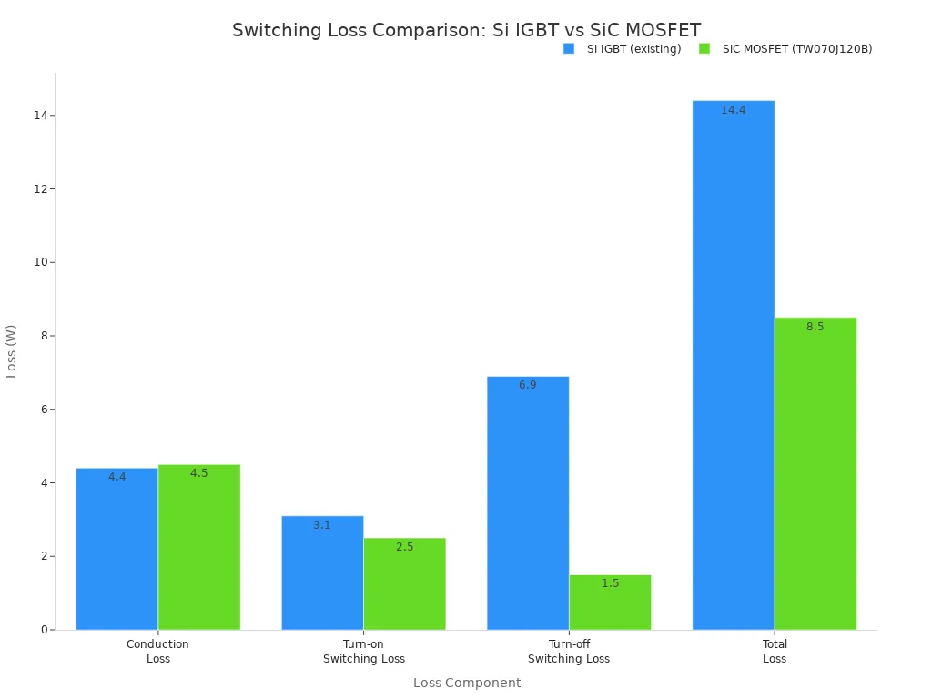
Each turn-off of the SiC MOSFET showed about 78% less energy loss than the similarly rated IGBT. Total loss fell by about 41%. In an electric vehicle traction inverter, swapping silicon IGBTs for SiC MOSFETs gives an efficiency gain of roughly 3–5% over a typical drive cycle. This improvement shows up most at low phase currents. At peak acceleration above about 700 A, the IGBT's low saturation voltage makes this gap smaller.
Silicon Carbide in Power Electronics and Modern Applications
Power Conversion for Electric Vehicles and Industrial Drives
Silicon carbide helps electric vehicles change and control energy better. SiC power modules boost how far cars can drive and how well they work. Third-generation SiC technology makes cars perform better, go farther, and charge faster. Companies now sell SiC power MOSFETs in types like M1 (1200 V, 1700 V) and M2 (650 V, 900 V) for traction inverters. Wolfspeed E-Series SiC MOSFETs are used in EV battery chargers and high-voltage DC/DC converters. ROHM's BSM600D12 SiC module beats IGBT modules in Formula E inverter tests and gives longer driving range.
Industrial drives also get better with silicon carbide power devices. The AVL SPECTRA Universal Inverter uses full SiC converters with switching speeds from 2 to 96 kHz. These systems can handle power up to 1,250 kW. SiC power MOSFETs cut switching losses a lot. A 1200 V SiC MOSFET cut total loss by about 41% compared to a silicon IGBT in tests. This efficiency gain means smaller cooling parts and more power in less space.
5G Infrastructure and Renewable Energy Systems
Silicon carbide semiconductors play a bigger role in 5G networks. GaN on SiC RF power amplifiers now appear in 5G macro base stations, small cells, and massive MIMO arrays. These devices let networks use higher frequencies and wider data paths for sub-6 GHz and millimeter-wave setups. Network operators save energy and have lighter radio units that are easier to put on towers.
Renewable energy systems use SiC power devices for better efficiency. SiC Schottky diodes remove boost diode switching losses in solar inverters. Normal silicon-based inverters reach about 96% average efficiency. Inverters with SiC devices reach up to 97.5%, cutting losses by up to 25%. A 60 kW boost converter design hit up to 99.5% peak efficiency. This material also lowers the cost of electricity below the DOE SunShot goal. SiC's effect on power electronics keeps growing in these key areas.
Future of SiC
Adoption Trends and Cost Reduction
Market Research Future says the SiC Power Semiconductor Market will grow at a CAGR of 23.42% from 2025 to 2035. Another report shows a 30.4% CAGR over the same period. The market size will rise from USD 3.5 billion to USD 50.1 billion. SNS Insider predicts a CAGR of 19.74% from 2025 to 2032. These numbers show strong demand across many sectors.
SiC uses go beyond electric vehicles. The material works in renewable-energy systems, industrial drives, aerospace, railway, and data-center applications. Its scalability allows high-power and high-temperature uses across industries. This adoption brings more investment in SiC technology.
Cost reduction is key to wider adoption. Moving from 150 mm to 200 mm wafers cuts cost per die by about 1.8 times. This makes SiC more affordable than silicon in power-conversion designs like solar inverters and industrial motor drives. Price parity with silicon is still a goal. Wafer boule yields must pass 70% to match silicon costs. Current yields sit at 45-55%. Reaching 70% would bring 200 mm SiC wafers within 1.5 times the cost of equal silicon substrates. The high capital intensity of fabrication plants—2 to 3 times that of similar silicon facilities—slows progress toward cost parity.
Ongoing Challenges in Manufacturing and Substrate Quality
Making high-quality SiC wafers brings lasting challenges. Several defect types limit yield. Micropipes and large-pit defects act as component killer defects, causing catastrophic leakage or breakdown. Basal plane dislocations (BPDs) cause forward-voltage drift in bipolar devices, leading to stacking faults that increase on-resistance. Carbon inclusions in epitaxial growth serve as nucleation sites for defects. Keeping substrate carbon inclusion density at 0.1-2.5 per square centimeter holds epitaxial defect density at or below 0.6 per square centimeter.
The industry relies on 6-inch silicon carbide substrate sizes for most production. These offer lower cost, lower defect rates, and mature processes. However, 8-inch silicon carbide substrate sizes promise cost advantages once yields improve. Right now, 8-inch wafers remain in early R&D or small-scale sampling stages. Low yields make 8-inch substrates possibly more expensive than 6-inch ones. Long-term prospects favor 8-inch as process maturity improves.
The silicon carbide substrate market must solve these yield and defect challenges. As manufacturing advances, SiC technology will reach more applications. The semiconductor material has proven its performance advantages. Cutting cost and improving quality will unlock its full potential in power electronics and beyond.
Silicon carbide (SiC) is a third-generation semiconductor material. Its wide bandgap, high thermal conductivity, and low switching losses make it special. These traits make SiC devices really important in power electronics. Electric vehicles, renewable energy systems, and 5G networks all gain from this technology.
Silicon carbide helps build smaller, cooler, and more efficient systems than silicon can. Engineers now see SiC as a must-have for next-generation electronics. Costs keep dropping as wafer sizes grow and yields get better. New uses include data centers and grid storage. Readers should look into SiC for their own designs.

Written by Jack Elliott from AIChipLink.
AIChipLink, one of the fastest-growing global independent electronic components distributors in the world, offers millions of products from thousands of manufacturers, and many of our in-stock parts is available to ship same day.
We mainly source and distribute integrated circuit (IC) products of brands such as Broadcom, Microchip, Texas Instruments, Infineon, NXP, Analog Devices, Qualcomm, Intel, etc., which are widely used in communication & network, telecom, industrial control, new energy and automotive electronics.
Empowered by AI, Linked to the Future. Get started on AIChipLink and submit your RFQ online today!
Frequently Asked Questions
What makes SiC different from silicon?
SiC has a bandgap wider than 3 eV. Silicon only has 1 to 1.5 eV. This gap lets SiC devices work at higher voltage, temperature, and frequency. SiC also moves heat about 3.3 times better than silicon. These traits make SiC a great pick for tough power electronics.
Why do electric vehicles use SiC devices?
SiC MOSFETs lower switching losses in EV inverters. A test showed total loss dropped by about 41% compared to silicon IGBTs. This gain helps cars drive farther and charge faster. SiC also lets automakers build smaller cooling systems. Companies like Wolfspeed and ROHM make SiC modules for traction inverters.
How does SiC improve solar and 5G systems?
SiC Schottky diodes remove boost diode losses in solar inverters. Efficiency goes up from about 96% to 97.5%. In 5G networks, GaN on SiC RF amplifiers power base stations and massive MIMO arrays. These devices handle higher frequencies and save energy. SiC helps operators build lighter radio units.
What challenges slow SiC adoption?
High wafer costs and defect rates hold back growth. Micropipes and basal plane dislocations hurt yields. Right now, boule yields sit at 45-55%. Reaching 70% would bring 200 mm SiC wafers closer to silicon prices. Moving from 150 mm to 200 mm wafers cuts cost per die by about 1.8 times.
Where is SiC technology heading?
The SiC power semiconductor market will grow at a 23.42% CAGR from 2025 to 2035. Costs keep falling as wafer sizes grow. New uses include data centers and grid storage. SiC will reach more industries as manufacturing matures. Engineers should check out SiC for next-generation designs.