Exploring Semiconductor Materials Types Properties and Production
Have you ever wondered what makes your smartphone think so fast? The answer lies in tiny parts called semiconductors. A semiconductor material works like a switchable bridge. Copper lets electricity flow freely. Rubber blocks it completely. A semiconductor can do both, depending on the situation. This special ability powers every electronic device you own.
This post explains the types, key traits, and making of these important materials. You will learn how engineers control their behavior. You will find out why silicon leads the industry. Silicon's abundance and dependability make it the clear winner. Its path from sand to supercomputer is amazing. Knowing about semiconductor materials helps you value the tech in your hands.
Key Takeaways
-
Semiconductors work like bridges that can turn on and off, controlling how electricity moves through all electronic devices.
-
Silicon leads the industry because it is plentiful, cheap, and works dependably.
-
Compound semiconductors like GaAs and GaN are great for high-frequency and high-power uses.
-
Doping adds impurities to pure semiconductors, which greatly boosts their ability to conduct electricity for use in devices.
-
Wide-bandgap materials like SiC and GaN allow for higher voltages, temperatures, and efficiency, helping to power future technology.
Types of Semiconductor Materials
You come across many kinds of semiconductor materials in today's electronics. Each type has its own job. Learning these groups helps you see why engineers pick certain materials for different tasks.
Elemental and Compound Semiconductors
Elemental semiconductors are made of just one element. Silicon and germanium are the two most common ones. These materials form the base of the electronics industry. Silicon leads because it is easy to find and cheap. Germanium was used early on in transistors but lost out to silicon because it cost more and had heat issues.
Compound semiconductors mix two or more elements from different parts of the periodic table. Gallium arsenide (GaAs) is a well-known example. It combines gallium with arsenic. Another key compound is gallium nitride (GaN). These materials have special traits that silicon cannot offer.
The main difference is in electron mobility. This number shows how fast electrons move through a material when voltage is applied. Higher mobility means faster device operation. The table below shows the electron mobility for three important semiconductor materials:
| Material | Electron Mobility (cm²/V·s) |
|---|---|
| Silicon (Si) | 1,500 |
| Germanium (Ge) | 3,900 |
| Gallium Arsenide (GaAs) | 8,500 |
You can see that gallium arsenide has much higher electron mobility than silicon. This edge makes GaAs great for high-frequency uses. The table below shows how different compound semiconductors perform in this area:
| Material | Key High-Frequency Property | Typical High-Frequency Application |
|---|---|---|
| GaAs | High electron mobility (~8500 cm²/V·s), low noise, stable above tens of GHz | 5G modules, Wi-Fi transceivers, satellite communication |
| GaN | Wide bandgap (3.4 eV), fast carrier drift velocity, low switching loss | 5G infrastructure, communication base stations, high-efficiency power systems |
Semiconductors with a wide band gap (greater than 2 eV) can work at higher voltages and temperatures. They are perfect for high-frequency and power electronics applications.
Compound semiconductors like GaAs and GaN shine where silicon falls short. They handle higher frequencies, run at higher temperatures, and switch power more efficiently. These benefits make them vital for modern communication systems and power electronics.
Intrinsic, Extrinsic, and Organic Semiconductors
Semiconductor materials also split by how pure they are. Intrinsic semiconductors are very pure. They have almost no impurities. In this pure state, the material does not conduct electricity well. The number of charge carriers depends only on temperature. At room temperature, intrinsic silicon has very few free electrons. This limits its use for semiconductor devices.
Extrinsic semiconductors change this through doping. Doping adds tiny amounts of other elements into the crystal structure. This process greatly boosts conductivity. The added impurities create extra charge carriers. Engineers control the doping process carefully to get the desired electrical traits. This control makes extrinsic semiconductors the base of most semiconductor devices.
The purity of the starting material matters a lot. Silicon used in electronics reaches amazing purity levels. Manufacturers purify silicon to "eleven nines" or 99.999999999%. This extreme purity ensures steady behavior. Any impurity can disturb the delicate crystal structure. The purification process removes nearly all contaminants. This level of purity directly affects device performance and reliability.
Organic semiconductors are a new category. These materials contain carbon-based molecules. They offer flexibility and low-cost production. You find them in some display technologies and experimental solar cells. However, organic semiconductors currently have lower performance than inorganic options. Their electron mobility stays far below silicon or gallium compounds. Researchers keep improving these materials for future uses.
The choice of semiconductor material depends on the application. Silicon works well for most digital logic and memory. Compound semiconductors handle high-frequency communication. Wide-bandgap materials like GaN excel in power conversion. Each material type brings specific strengths to semiconductor devices.
Gallium-based compounds show great promise for power electronics. The comparison below highlights why GaN beats silicon in this field:
| Property | Silicon (Si) | Gallium Nitride (GaN) |
|---|---|---|
| Bandgap (eV) | 1.12 | 3.4 |
| Critical Field (MV/cm) | 0.3 | 3.3 |
| Electron Mobility (cm²/V·s) | 1450 | 1500-2000 |
| Switching Frequency | Low (<100 kHz) | High (1-10 MHz) |
These differences turn into real benefits for power systems:
-
Faster Switching Speed: GaN devices switch much faster than silicon, letting power converters run at higher frequencies. This leads to smaller inductors and capacitors, smaller system size and weight, and better power density.
-
Lower Power Loss: GaN devices have lower conduction and switching losses than silicon. This directly means higher energy efficiency, less heat, and better system performance.
-
Higher Overall Efficiency: By combining higher voltage ability, faster switching speeds, and lower power losses, GaN allows power systems that are much more efficient than old silicon designs, leading to less energy use and lower running costs.
Understanding these material groups helps you see why your phone uses silicon for its processor but gallium compounds for its wireless communication. Each semiconductor material has a specific role. The traits of each material decide its best uses. As technology moves forward, you will see new materials join this family. The growth of semiconductor materials keeps pushing the limits of what electronic devices can do.
Key Semiconductor Properties and Performance
Semiconductor properties decide how a material works in real devices. Bandgap, mobility, and heat traits control the final performance. These features guide engineers when they pick materials for certain jobs. You need to know these traits to see why different materials fit different tasks. Semiconductor properties like bandgap affect performance directly.
The Role of Bandgap
The bandgap is the energy gap between the valence band and the conduction band. This gap decides if a material acts as a conductor, semiconductor, or insulator. A large bandgap means electrons need more energy to jump. Insulators have very large bandgaps. Conductors have no bandgap. Semiconductors fall in between. Bandgap size directly affects device uses. Silicon has a bandgap of 1.12 eV. This works well for most digital logic. Wide bandgap semiconductors like silicon carbide and gallium nitride have bandgaps above 3 eV. These materials have a critical electric field density about ten times higher than regular semiconductors. This trait lets them handle much larger electric fields before breakdown. It directly allows operation at higher voltages in power devices.
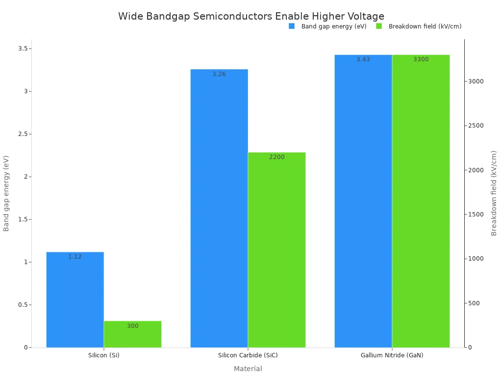
Bandgap also affects working temperature. Wide bandgap semiconductors can run at high temperatures often above 200°C without losing much performance. Narrow bandgap semiconductors usually struggle at high temperatures. The bandgap energy of semiconductors drops as temperature rises. Higher temperatures boost intrinsic carrier generation. This raises leakage current and can cause early breakdown. Since intrinsic carrier density falls exponentially with wider bandgap, they show much lower leakage current. This lets them handle higher working temperatures and higher voltages without failure.
Conductivity and Thermal Characteristics
Electron mobility is a key semiconductor property. Mobility measures how fast electrons move through a material. Higher mobility means faster device operation. Silicon has electron mobility of 1,500 cm²/V·s. Gallium arsenide has 8,500 cm²/V·s. This shows why GaAs works better for high-frequency uses. Mobility directly affects performance in semiconductor devices. The higher the mobility, the faster the switching speed. This impacts overall efficiency in power conversion systems.
Thermal conductivity also matters a lot. Heat management is vital for modern electronics. Silicon conducts heat fairly well. However, some wide bandgap materials like silicon carbide have excellent thermal conductivity. This lets them handle more power without overheating. These traits make SiC ideal for electric vehicles and industrial power systems. The mix of wide bandgap, high mobility, and good thermal conductivity creates semiconductors with top performance. You see these benefits in smaller power supplies, more efficient chargers, and reliable high-temperature electronics. Knowing these semiconductor properties helps you see why different materials fit different uses. Semiconductor devices depend on these traits for reliable operation.
The Production Process of Silicon Wafers
Silicon leads the semiconductor industry because it is plentiful and easy to process. You can find silicon in sand and quartzite, making it one of the most common elements on Earth. This raw material starts an amazing trip to become the base of modern electronics. The production process needs incredible accuracy at every step.
Purification and Crystal Growth
The trip starts with metallurgical-grade silicon at about 98% purity. This material conducts electricity too unevenly for semiconductor use. You need much higher purity to build reliable devices. The industry standard reaches "eleven nines" — a purity level of 99.999999999%. At this extreme purity, silicon becomes almost non-conductive. Even tiny impurities can disturb electrical behavior in unexpected ways.
The purification process follows several key steps:
-
Chemical purification: The Siemens process turns silicon into silicon tetrachloride (SiCl₄), cleans it, then breaks it down. A fluidised bed reactor offers another way using hydrogen to make silane (SiH₄), followed by cleaning and breakdown.
-
Zone refining: A heated zone moves along a silicon rod. Impurities solidify at the cooler end and stay behind. Doing this step again raises purity further.
-
Crystal growth: The Czochralski process makes a single crystal. You place a seed crystal into melted silicon, then slowly pull and spin it. This pulls pure silicon into a large single crystal with very few impurities.
Several factors control crystal quality during the Czochralski process:
-
Temperature control: Exact regulation keeps the melt and crystal boundary stable.
-
Rotation speeds: Both crystal and crucible spinning affect fluid flow and heat balance.
-
Withdrawal rate: The pull speed directly changes crystal width and defect formation.
-
Computerized monitoring: Automated systems watch melt level, adjust pull rates, and spot defects in real time.
These controls help the crystal grow evenly. The final ingot can be several meters long and weigh hundreds of kilograms. This single crystal forms the starting point for all silicon wafers used in chip making.
Wafer Slicing and Preparation
After you grow the ingot, you must turn it into thin, flat discs. The slicing process uses diamond-coated wire saws to cut the ingot into separate wafers. Each wafer is about 775 µm thick for 300mm diameters — the main size for advanced logic and memory chip making. This thickness balances strength with material use.
After slicing, wafers go through several preparation steps. Grinding removes saw damage from the cutting process. Edge rounding stops chipping during handling. Then chemical mechanical polishing (CMP) creates a mirror-smooth surface. This polishing reaches near-atomic flatness. Micro-roughness on polished silicon wafers often measures below 1 nm RMS for advanced semiconductor applications.
Micro-roughness on polished silicon wafers is often measured below 1 nm RMS for advanced semiconductor applications.
The final cleaning step removes any leftover particles or metal dirt. A clean surface matters because integrated circuits form directly on this base. Any flaw can ruin whole batches of chips. The quality of this surface directly affects yield and device performance.
The whole production process turns ordinary sand into precision-made substrates. Each step builds on the last one, needing exact standards throughout. This manufacturing chain creates the base for nearly every electronic device you own. The purity gained through these steps enables the amazing performance of modern semiconductor materials. Without this careful production, the semiconductor industry could not work at its current size.
Future Trends in Semiconductor Materials
The semiconductor industry keeps changing. Engineers always push materials to do more. You will see big changes soon. These advances will change electronics, cars, and communication systems.
The Rise of Wide-Bandgap Semiconductors
Silicon has worked well for many years. But it hits physical limits in high-power uses. Wide-bandgap materials like silicon carbide (SiC) and gallium nitride (GaN) are now becoming important. Their larger bandgap lets them work at higher voltages, temperatures, and frequencies than silicon.
The market shows this change. The silicon carbide semiconductor device market is growing fast:
| Metric | Value |
|---|---|
| 2025 Market Size | USD 3.83 Billion |
| 2030 Projected Market Size | USD 12.03 Billion |
| CAGR (2025-2030) | 25.7% |
This growth comes from real performance gains. GaN power supplies show clear advantages over silicon-based designs:
| Metric | Silicon-based | GaN-based | Gain |
|---|---|---|---|
| Power density | 5.3 W/in³ | 11.4 W/in³ | More than doubled (2.15x) |
| Weight | 820 g | 560 g | 32% reduction |
| Reverse recovery losses | Present (body diode) | Near-zero (no body diode) | Eliminates additional switching losses |
These improvements matter for electric vehicles and 5G networks. GaN devices switch faster and waste less energy as heat. This efficiency means smaller chargers, longer battery life, and more reliable power systems. The compound semiconductors SiC and GaN have special traits that silicon cannot match. Their wide bandgap allows higher breakdown voltage and better heat handling. You will see these materials in fast-charging stations, solar inverters, and radar systems.
Exploring New Material Frontiers
Beyond wide-bandgap materials, researchers explore entirely new kinds of semiconductor materials. Graphene is a very promising candidate. This single layer of carbon atoms moves electrons extremely fast. Its electron mobility reaches 200,000 cm²/Vs, compared to just 1,400 cm²/Vs for silicon.
World's First Graphene Semiconductor Outperforms Silicon Chips In a recent study in Nature, Georgia Tech researchers developed the world's first functional graphene semiconductor by growing it on silicon carbide wafers and doping it to create transistors. The study demonstrated that electrons flow through graphene more efficiently than silicon, potentially leading to faster and more efficient computers.
This breakthrough opens doors for quantum computing and advanced sensors. Graphene-based semiconductors could change artificial intelligence chips and flexible electronics. The material's unique traits allow full transistor shutdown, meeting strict digital electronics needs.
Researchers also study transition metal dichalcogenides. These 2D materials offer adjustable bandgaps and great mechanical flexibility. They promise to push miniaturization past silicon's limits. The future of semiconductor materials looks bright. Each new discovery brings faster, more efficient devices. You will benefit from these advances through better phones, cleaner energy, and smarter technology.
The journey from sand to smartphone shows how remarkable semiconductor materials truly are. You hold the result of extreme purification, precise crystal growth, and careful doping in your hand. Every call, photo, and search depends on these invisible switches working billions of times per second.
The semiconductor industry continues expanding rapidly. According to Statista, the global semiconductor market is projected to reach US$1.29 trillion by 2030. This growth reflects silicon's enduring role in electronics and new materials like GaN and SiC finding fresh applications. Silicon remains the foundation, while innovative compounds push boundaries.
Future innovations will bring faster devices, cleaner energy, and smarter technology. The evolution of semiconductor materials drives every technological breakthrough you will experience. Each new semiconductor discovery powers the next generation of devices you will use daily.

Written by Jack Elliott from AIChipLink.
AIChipLink, one of the fastest-growing global independent electronic components distributors in the world, offers millions of products from thousands of manufacturers, and many of our in-stock parts is available to ship same day.
We mainly source and distribute integrated circuit (IC) products of brands such as Broadcom, Microchip, Texas Instruments, Infineon, NXP, Analog Devices, Qualcomm, Intel, etc., which are widely used in communication & network, telecom, industrial control, new energy and automotive electronics.
Empowered by AI, Linked to the Future. Get started on AIChipLink and submit your RFQ online today!
Frequently Asked Questions
Why is silicon so popular in the semiconductor industry?
Silicon is common, so it is cheap and easy to get. You find it in regular sand. Its processing methods have been improved over many years. This means makers can produce silicon wafers with very pure and consistent properties. No other semiconductor material has both low cost and reliable performance.
What is different about wide-bandgap semiconductors?
Wide-bandgap materials, such as silicon carbide and gallium nitride, can work with higher voltages and temperatures than silicon. Their bigger bandgap lets electrons move with more power. This allows faster switching and better energy use in power electronics. You find these materials in electric cars and 5G networks.
How does doping affect a semiconductor?
Doping puts very small amounts of other elements into a pure semiconductor crystal. These added impurities make more charge carriers. This greatly boosts conductivity. Engineers carefully control doping to get the right electrical properties. Without doping, you cannot make transistors, diodes, or integrated circuits from silicon.
Can organic semiconductors take the place of silicon?
Organic semiconductors are flexible and cheap to make. You see them in some screens and test solar cells. But their electron mobility is much lower than silicon's. This limits their use in fast devices. Researchers keep working on organic materials, but silicon is still the main choice for now.
How does thermal conductivity affect device performance?
Handling heat directly affects how fast and steady a semiconductor works. Materials with high thermal conductivity, such as silicon carbide, get rid of heat well. This lets them handle more power without getting too hot. Silicon conducts heat fairly well, but wide-bandgap materials are better in tough jobs like electric car power systems.