The Complete IC Manufacturing Process Explained
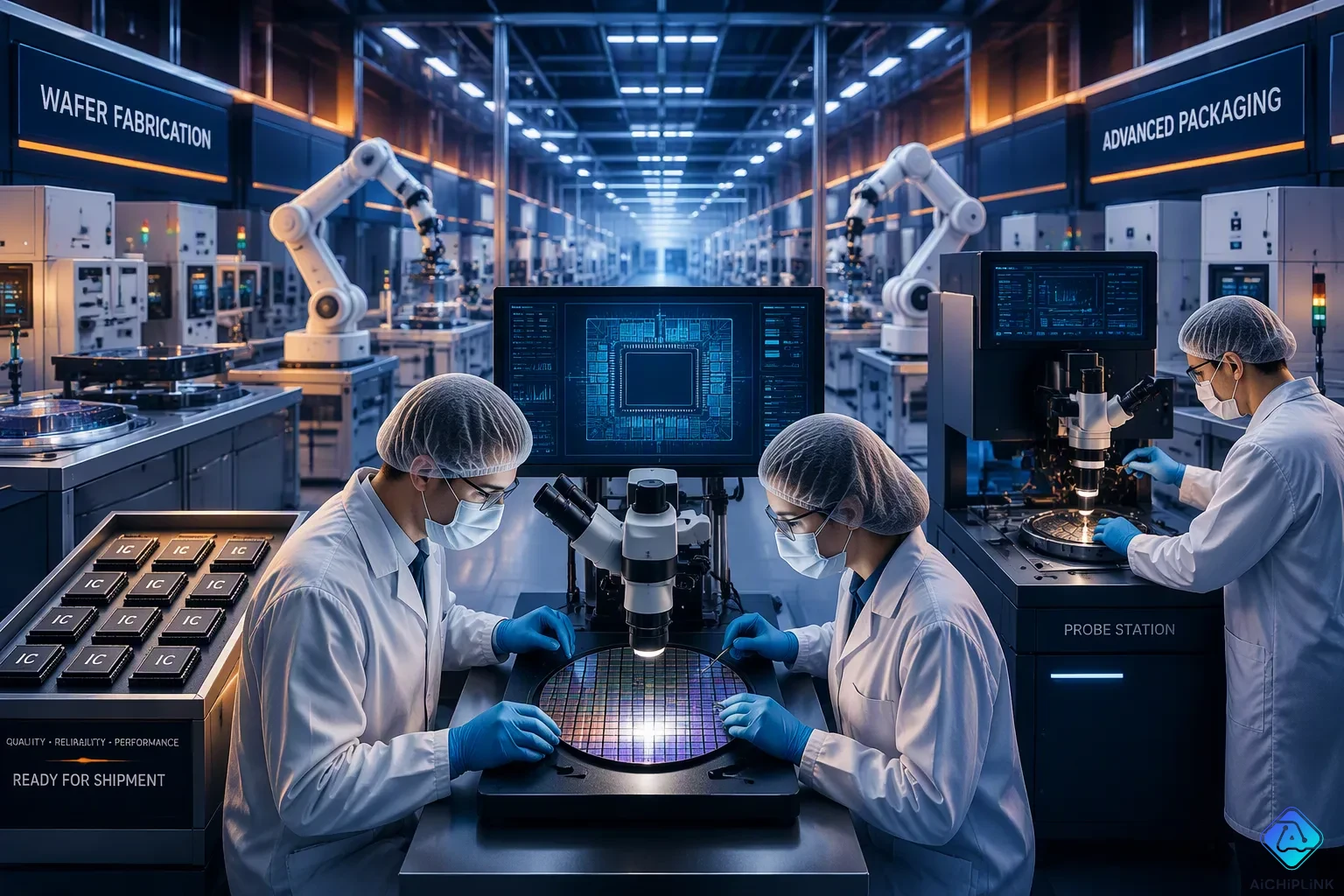
You find integrated circuits in almost every device you use every day. The IC manufacturing process changes raw silicon into working chips using exact steps, and at the heart of this lies Integrated Circuits production—a discipline that demands incredible precision. This process needs amazing miniaturization, packing billions of transistors onto a single integrated circuit. You make the chips inside tightly controlled clean rooms, where even a speck of dust ruins a chip. The whole process includes design, fabrication, testing, and packaging, with Integrated Circuits production serving as the backbone that ties these stages together. Each step builds on the last, turning simple silicon into powerful electronics. Understanding this process shows how your smartphones and medical devices work. The level of precision in Integrated Circuits production keeps pushing limits, enabling faster and more efficient technology. As you look at each step, you'll see the complexity behind every electronic device you use.
Key Takeaways
-
Integrated circuits begin as designs on a computer, then become patterns on expensive masks.
-
Silicon wafers need to be very pure, with impurities under one part per billion.
-
Photolithography uses light to print very small patterns, which lets us fit billions of transistors on a single chip.
-
Testing and packaging protect and check each chip, making sure only working chips reach you.
IC Manufacturing Process: Design and Silicon Wafer Preparation
Circuit Design and Mask Creation
Every integrated circuit starts as a plan. Engineers draw billions of transistors on computer screens, showing how each part connects and talks to others. This design stage sets the whole process, because any mistake here gets worse in every later step. You turn the final plan into a set of photomasks, which work like stencils for light. Each mask holds one layer of the circuit pattern, and a modern chip may need many of these layers stacked exactly on top.
The cost of these masks goes up with complexity. For a 5nm process node, you need about 70 to 80 masks, and the price is between $6 million and $12 million. Advanced extreme ultraviolet lithography and special pellicles cause much of that cost. You use these masks many times during making, so their quality directly affects your success rate. One tiny flaw in a mask can ruin thousands of chips.
| Process Node | Mask Count | Cost Range | Notes |
|---|---|---|---|
| 5nm | ~70-80 | $6M-$12M | Heavy EUV usage; advanced pellicles |
Purifying Silicon and Growing Ingots
Your starting material is sand, but normal sand does not work. You must clean raw silicon to a very high level. Electronic-grade silicon reaches a purity of 99.9999999%, called "nine nines." Impurity levels drop below one part per billion. This extreme purity matters because even tiny unwanted atoms mess up the electrical behavior of semiconductors. You melt the cleaned polycrystalline silicon in a furnace and slowly pull a seed crystal upward. The melted material hardens around the seed, forming a single round crystal called an ingot.
Modern factories grow ingots that are 300mm across, matching the standard wafer size. The industry spent many years getting to this size, and no larger size has become standard yet. You grind the ingot to a precise target diameter with a tolerance of ±0.5mm, then add a notch marker for alignment. Finally, you cut the ingot into thin silicon wafers using diamond saws. Each wafer gets polished and cleaned before moving to the next step. This silicon wafer making step needs total control, because the quality of your wafers sets the base for every device you build. The whole manufacturing process depends on this preparation, and silicon integrated circuits get their performance from the purity of the starting material.
Photolithography and Doping in Integrated Circuits Production
Photolithography forms the heart of integrated circuits production. You use ultraviolet light to transfer patterns onto silicon wafers. This step defines every transistor and connection on your integrated circuit. The entire manufacturing process depends on getting these patterns right. Without photolithography, you cannot build the complex layers that make modern semiconductors work. Each pattern you create becomes part of a larger structure, and the accuracy of this step determines your final chip performance.
Patterning with Light and Etching
You start by coating the wafer with a light-sensitive material called photoresist. Then you align the silicon under a photomask and shine ultraviolet light through it. The light changes the photoresist, making some areas soluble. You wash away the soluble parts, leaving a pattern on the silicon. This pattern matches the circuit design you created earlier. The entire integrated circuits production line depends on this transfer accuracy.
State-of-the-art systems use extreme ultraviolet (EUV) light for the smallest features. The wavelength is incredibly short.
The SPIE Optipedia article specifies that EUV lithography operates at a wavelength of approximately 13.5 nm, noting this particular choice enables efficient multilayer mirror optics.
This short wavelength lets you print features below 7 nm. However, the equipment costs a tremendous amount.
| Source | Cost per EUV machine |
|---|---|
| Eureka Patsnap (Intel investment) | $150–200 million |
| Eureka Patsnap (initial capital expenditure) | $120–150 million |
| GM Insights (single EUV scanner) | >$200 million |
After patterning, you etch the exposed areas. You use plasma or chemicals to remove material where the photoresist is gone. This transfers the pattern into the silicon or other layers below. The resolution of current systems determines how small you can make these features.
| Scanner Type | NA Value | Resolution Limit (Half-Pitch) | Corresponding Pitch |
|---|---|---|---|
| Current EUV (ASML NXE:3400B) | 0.33 | 13 nm | 26 nm |
| High-NA EUV (Future) | 0.55 | 8 nm | 16 nm |
You repeat this pattern-and-etch cycle many times. Each layer builds on the last, creating the three-dimensional structure of your integrated circuits.
Doping and Layer Deposition
Doping introduces impurities into the silicon to change its electrical properties. You add boron to create p-type regions. You add phosphorus or arsenic to create n-type regions. These regions form the transistors that make up your IC. The integrated circuits production process relies on precise doping control.
Commercially available silicon wafers show typical resistivity ranges that correspond to doping concentrations. N-type wafers (phosphorus-doped) have resistivities of 1–50 Ω-cm, while p-type wafers (boron-doped) have resistivities of 1–30 Ω-cm. These resistivity values are inversely related to dopant concentration.
-
P-type (boron doping): Hole concentration ranges from 10¹⁵ to 10²⁰ cm^-3, with a caution that concentrations above 10¹⁹ cm^-3 can reduce hole mobility.
-
N-type (ion implantation of arsenic or phosphorus): Typical doses are 10¹⁵ to 10¹⁶ cm^-2 at energies of 10–100 keV, producing peak dopant concentrations from 1×10²⁰ to 2×10²⁰ cm^-3.
You follow doping with layer deposition. You add thin films of insulating or conductive materials. Atomic layer deposition (ALD) gives you precise control over film thickness. Each cycle adds just one atomic layer at a time.
| Substrate Type | Typical Uniformity |
|---|---|
| Low aspect ratio (e.g., wafers) | <1% to 1% |
| High aspect ratio | <4% |
You repeat deposition, patterning, and doping many times. Each cycle builds another layer of your integrated circuit. The entire fabrication occurs inside a clean room to prevent contamination. Even a single dust particle can ruin your devices. This repeated process creates the complex structures that power modern electronics. The precision of integrated circuits production keeps improving, enabling smaller and faster ICs. As you continue through the semiconductor manufacturing flow, you see how each step depends on the one before it. The silicon you start with becomes something extraordinary. Every integrated circuit you design requires this exact sequence. Your devices demand this level of precision. The manufacturing techniques you use today define what tomorrow's technology can achieve.
Metallization, Testing, and Dicing of Wafers
Building Interconnects and Metallization
You have built the transistors, but they cannot work alone. They need wires to connect them into a working integrated circuit. This step, called metallization, makes those conductive paths. You lay down thin metal films across the silicon surface, then pattern them using the same photolithography methods from earlier. Copper has become the standard metal for these connections because it carries electricity well.
You build these interconnects in layers. Each layer moves signals across the chip. Vertical links, called vias, join one layer to the next. A typical 7nm logic chip uses up to 15 total back-end-of-line metal layers. You need 3 to 6 local interconnect layers for the shortest links between nearby transistors. The remaining layers carry power and longer signals across the whole integrated circuit.
| Process Maturity Stage | Typical Yield Range | Specific Example |
|---|---|---|
| Initial Development | 0-20% | - |
| Process Optimization | 20-50% | - |
| Early Production | 50-70% | - |
| Commercial Viability (Mature) | 70-90% | TSMC 3nm: ~80%; TSMC 5nm: ~90% |
Copper interconnects in advanced CMOS have a maximum DC current density of approximately 1–3 × 10^6 A/cm² (10–30 MA/cm²) for modern dual-damascene copper with barrier metals.
You must respect this current limit during design. Push too much current through a thin wire, and it fails. The metal slowly moves over time, creating gaps that break the connection. This effect, called electromigration, sets a hard limit on your design choices. You balance wire thickness against the current each signal must carry.
The metallization process also includes a barrier layer around each copper wire. Copper atoms spread easily into silicon and harm transistor behavior. You add a thin barrier metal, usually tantalum or titanium compounds, to stop this spread. The barrier adds resistance, so you keep it as thin as possible while still doing its job.
Wafer Testing and Dicing
After you finish all metal layers, the wafers contain hundreds of complete integrated circuits. You cannot see which ones work just by looking. You need electrical testing to find the good devices. You place the wafer on a precision stage and lower a probe card onto each chip. The probe card has tiny needles that touch the bond pads on your integrated circuit. You apply test patterns and measure the responses.
This testing step finds defective chips before you spend money packaging them. The yield rate tells you what fraction of chips pass. A mature manufacturing process typically achieves 70% to 90% yield. TSMC's 5nm process reaches about 90% yield, while their 3nm process sits near 80%. Early development runs often start below 20% yield. Engineers work through process optimization to push that number higher.
You mark the defective chips with a small ink dot or record their positions in a digital map. Then you dice the wafer into individual rectangular pieces called dies. You use a diamond-bladed saw that cuts along the scribe lines between chips. The silicon wafers are thin and brittle, so you must control the cutting speed carefully. You mount the wafer on adhesive tape during dicing to hold the dies in place after cutting.
The dicing process produces individual dies ready for packaging. Each die contains one complete integrated circuit. You discard the defective ones based on your test results. The good dies move to the next stage, where they receive protective packaging and external connections. This entire fabrication flow, from metallization through testing and dicing, transforms your silicon into usable ICs. Every step you perform here directly affects the final quality and reliability of your devices. The precision you maintain during these operations determines whether your integrated circuits perform as designed.
Packaging and Final Inspection of Integrated Circuits
Die Attachment and Wire Bonding
You now have individual dies from the processed wafers. Each die is a fragile integrated circuit that needs protection. You mount it onto a package substrate. You use conductive epoxy to bond the die to the substrate. Silver-filled conductive epoxies work well for high-power devices. They contain 75–85% silver filler by weight. Electrical resistivity after curing ranges from 5 × 10⁻⁵ to 5 × 10⁻⁴ Ω·cm. Thermal conductivity reaches 3–10 W/mK.
After attachment, you create electrical connections from the die to the package leads. You use wire bonding for this task. Fine gold or copper wires connect the bond pads on the die to the substrate. The wire bonding process requires precision alignment. Today's technology operates at pitches below 40 microns. This precision lets you pack many connections into a small area. The bond head moves quickly, placing each wire in sequence. You control the loop height and shape carefully. Proper bonding ensures reliable signal paths for your integrated circuit. This entire assembly requires careful handling of the silicon die from the wafers.
Encapsulation and Final Quality Control
The bonded integrated circuit needs protection from moisture, dust, and mechanical stress. You encapsulate it in a plastic molding compound. The most common material is Novolac-based epoxy. It has a thermal conductivity of 0.67 W/mK and a glass transition temperature of 150°C. This epoxy surrounds the die and wires, forming a solid protective shell. You transfer the compound into a mold cavity under heat and pressure. The material hardens and seals everything inside. The encapsulation process protects the delicate silicon structure.
Advanced packaging technologies for integrated circuits continue to grow. The fan-out wafer-level packaging market reached USD 35.6 billion in 2024. It should reach USD 63.5 billion by 2029, growing at 12.3% annually. Major players dominate this space.
| Company | Market Share (%) |
|---|---|
| TSMC | 17.0 |
| ASE | 14.0 |
| Amkor | 12.5 |
| Top 5 combined | 58.5 |
This concentration shows how specialized packaging has become.
Final quality control verifies every packaged device. You test for electrical continuity, insulation resistance, and signal integrity. You also perform thermal cycling and humidity tests. You examine packages under microscopes for cracks or voids. Only devices that pass all tests ship to customers. This rigorous process ensures your silicon integrated circuits perform as designed. The manufacturing journey ends here, but quality control guarantees your devices meet specifications. Each packaged integrated circuit represents the culmination of a complex ic fabrication flow.
The journey from raw silicon to a packaged chip demands precision at every turn. Each step in the ic manufacturing process builds upon the last, transforming simple material into powerful electronics. The integration of design, fabrication, and packaging enables the performance of modern devices, from smartphones to medical equipment.
Advancements in integrated circuits production continue pushing boundaries. The International Roadmap for Devices and Systems projects 5nm nodes with an 18nm gate length and 51nm contacted gate pitch. These shrinking dimensions drive innovation across the silicon chip industry.
| Parameter | Projected Value for 5nm Node |
|---|---|
| Gate length | 18 nm |
| Contacted gate pitch | 51 nm |
| Tightest metal pitch | 30 nm |
Every integrated circuit you touch represents this remarkable process. Explore advanced lithography techniques or clean room operations to deepen your understanding of these electronic devices.

Written by Jack Elliott from AIChipLink.
AIChipLink, one of the fastest-growing global independent electronic components distributors in the world, offers millions of products from thousands of manufacturers, and many of our in-stock parts is available to ship same day.
We mainly source and distribute integrated circuit (IC) products of brands such as Broadcom, Microchip, Texas Instruments, Infineon, NXP, Analog Devices, Qualcomm, Intel, etc., which are widely used in communication & network, telecom, industrial control, new energy and automotive electronics.
Empowered by AI, Linked to the Future. Get started on AIChipLink and submit your RFQ online today!
Frequently Asked Questions
What is a clean room, and why do you need one?
A clean room filters air to remove dust. Even one tiny speck can ruin an integrated circuit. You keep temperature and humidity steady inside these rooms to protect your devices during fabrication.
How long does the entire manufacturing process take?
The full journey from design to packaged chip takes several weeks. Complex integrated circuits need many layers, and each layer requires multiple steps. You move wafers through hundreds of process steps before finishing.
What is yield, and why does it matter?
Yield shows the percentage of working chips on a wafer. A mature process like 5nm reaches about 90% yield. Higher yield means lower cost per working chip. You watch yield closely to improve your manufacturing process.
Why do you use silicon for making chips?
Silicon is plentiful and works well as a semiconductor. You can purify it to extreme levels, reaching 99.9999999% purity. This purity ensures consistent electrical behavior in your finished devices.