AOI vs. X-Ray Inspection for PCB Assembly
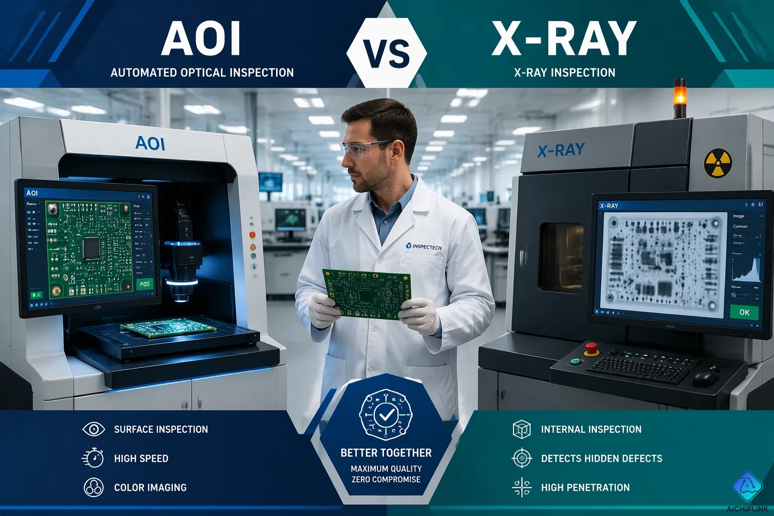
AOI is the fastest choice for visible surface defects in high-volume runs. X-ray inspection is a must for hidden solder joints in complex packages like BGA. Many manufacturers use both. This comparison of AOI vs. X-ray inspection covers where each technology comes from, what defects it finds, speed, and cost. It then gives practical tips for choosing in PCB assembly quality control. AOI catches up to 95% of surface-level defects. AXI reaches up to 99% on hidden joints and voids. Those numbers shape every decision in any aoi vs x-ray evaluation for PCB assembly.
Key Takeaways
-
AOI uses light to find surface defects quickly and cheaply.
-
X-ray sees through packages to catch hidden joint problems.
-
AOI is fast and costs less, making it great for high-volume lines.
-
X-ray is slower and pricier but essential for complex boards.
-
Using both AOI and X-ray gives the best quality control.
AOI vs X-Ray in PCB Manufacturing and Assembly
The Short Answer
The one-line verdict is simple. AOI wins on visible surface defects and speed. X-Ray wins on hidden joints and complex packages. Both are non-contact methods, so neither one touches or stresses the board. That shared trait makes them easy to place inline or offline without disturbing the production flow.
The choice between AOI and X-Ray inspection depends on what the camera or the detector can physically reach. AOI sees the top of the board. X-Ray sees through it. A team that compares aoi vs x-ray inspection should start with that physical limit, not with price tags or vendor claims.
Why Both Exist
X-Ray is not necessary for every board. Simple boards with visible joints may rely on AOI, visual inspection, and in-circuit testing alone. Those three methods cover opens, shorts, missing parts, and wrong values on a single-sided or low-density design. Adding AXI to that line raises cost without adding much coverage.
Complex boards change the math. Once a design hides joints under a package body, optical tools lose their view. That gap is why both methods exist in modern pcb manufacturing and assembly. A shop that runs only AOI accepts a blind spot. A shop that runs only X-Ray pays for speed it may not need. Most pcb assembly quality control plans mix the two, and the mix follows the board, not the budget alone.
How AOI and X-Ray Work
Light Source vs. X-Ray Source
The two methods begin with different science. Automated optical inspection uses a light source and high-resolution cameras to take pictures of the board. LED light at many angles and wavelengths helps surface contrast. Automated x-ray inspection uses X-rays that go through the board instead of bouncing off it. The beam follows Beer-Lambert attenuation, so ray strength drops based on material thickness and atomic number.
That gap sets what each tool can reach. Light cannot pass through black epoxy or shielding, so automated optical inspection pcb work stops at the visible surface. X-rays go through packages such as BGAs and QFNs and show the joints underneath. A quick comparison makes the split clear:
| Aspect | AOI Light Sources | X-ray Sources |
|---|---|---|
| Imaging principle | Optical reflection with cameras and LED light | X-ray penetration with density contrast |
| Penetration | Surface only | Internal structures and hidden areas |
| Resolution | Micron-level detail on exposed joints | Density-based internal detail |
| Core limitation | Cannot see beneath BGAs or shielding | Slower; weak at surface color and text |
Surface Imaging vs. Volumetric Imaging
Surface imaging captures what the eye could see with enough magnification. AOI picks out features down to microns on exposed surfaces, which fits visible solder joints and component bodies. The method cannot judge a joint it cannot view, so hidden cracks and voids stay unseen.
Volumetric imaging works from the inside out. In automated x-ray inspection, the beam goes through the board, and different materials absorb it in different ways. That contrast shows hidden defects, and software studies the result. Some systems add computed tomography to make 3D x-ray imaging for complex failure analysis. This volumetric view is why aoi and axi work well together in pcb manufacturing and assembly. AOI covers the surface, and AXI covers the volume beneath it. Teams that treat x-ray inspection technology as a swap for optical tools miss that division of labor. Each method answers a question the other cannot.
AOI vs. AXI: Defect Detection
The main differences between AOI and AXI are easiest to see in what each method can actually reach. Automated optical inspection looks at the surface of the board. Automated x-ray inspection looks through the package body. That split decides which defects each tool catches. It also explains why defect detection plans for pcb assembly rarely depend on one method alone.
Visible Defects AOI Catches
Automated optical inspection is great at surface-level problems. The system compares each board against known-good data. Then it flags changes in shape, color, and position. Common defects in pcb assembly that AOI catches include missing components, wrong parts, polarity reversal, solder bridging, tombstoning, component offset, insufficient solder, lifted leads, wrong orientation, and stray solder balls. Each of these defects leaves a visible mark, so a camera and lighting setup can catch it.
Some AOI systems can achieve defect detection rates of over 99%, significantly reducing the risk of faulty boards reaching the market.
Three-dimensional AOI adds height and volume data to the optical check. That extra dimension lets the system judge solder joint quality, coplanarity, and lifted leads that a flat 2D image would miss. The tradeoff is higher cost and, on some systems, a slower cycle time. For most high-volume surface-mount work, though, AOI remains the first line of defense against solder defects and placement errors.
Hidden Defects X-Ray Reveals
X-ray inspection covers the blind spots. BGA and chip-scale packages hide their joints under the body, so optical tools cannot judge them. AXI detects the most common BGA problems through their visual signatures:
-
Solder bridges, the most common defect seen under transmissive real-time X-ray with tilt
-
Gross or excessive voids, visible at higher power and magnification
-
Misalignment or a shifted BGA package
-
Missing or broken solder balls
-
Head-in-pillow defects, detectable when the equipment tilts the sample or detector
-
Opens and voids, which sometimes need trained technicians to confirm
X-ray inspection is one of the most effective methods for evaluating BGA solder joints because the connections are completely hidden beneath the package body. X-ray systems can detect voiding, bridging, open joints, head-in-pillow defects, insufficient solder, and ball misalignment.
Solder voids in BGA and CSPs deserve special attention. IPC-A-610 typically sets acceptable BGA void limits below 25%, and x-ray inspection verifies compliance against that limit.
| Void Range | Classification |
|---|---|
| 0–10% | Typical baseline from normal flux outgassing |
| 10–15% | Borderline; begin investigation |
| 15–25% | Elevated; approaching the commonly cited limit |
| Above 25% | Outside the baseline; verify against the governing revision |
A trained operator reads these signatures and measures void percentages, ball dimensions, and joint geometry against acceptance criteria. That measurement step is where AXI earns its place in pcb assembly quality control.
Speed and Throughput
AOI Cycle Times
AOI is fast. A typical system checks a PCB in about 10–20 seconds. The optical process itself makes this speed possible. Cameras take a picture of the board surface in one pass, and software compares that image to a known-good reference. Nothing like beam scanning or depth rebuilding slows the cycle down.
Programming time adds to the total. An engineer has to teach the system the board layout, where parts sit, and what counts as acceptable. This setup takes hours for a new design. Once it is done, though, the program runs on its own. A well-tuned program also cuts false calls, which keeps operators from re-checking good boards. Inline bottlenecks rarely happen on high-volume lines. The AOI station keeps up with the placement machines upstream, so boards move through without waiting. That speed advantage makes AOI a natural fit for smt inspection on fast surface-mount lines.
AXI Throughput Limits
AXI runs slower. X-ray imaging is complex. The system has to create a beam, send it through the board, and rebuild the internal geometry. Each of those steps takes time. One board can tie up the station much longer than it would under an AOI camera.
Programming takes more work as well. An engineer has to set beam power, tilt angles, and magnification for each package type. The software then builds a 3D model to compare against. This setup can take days on a complex design. Inline bottlenecks show up when one AXI station serves several lines. Boards wait in line, and the station becomes the limit. A team that weighs aoi vs x-ray throughput has to accept this tradeoff. The slower cycle buys coverage that no optical tool can match. Shops that run both aoi and axi often put the AXI station offline or at the end of the line, where its slower pace does not hold up production. That layout keeps x-ray inspection in the quality plan without choking the main flow. A pcb assembly line that ignores this layout risk pays for it in stalled output.
Cost Factors
Equipment and Operating Costs
An AXI system costs far more than an AOI machine. The X-ray source, detector, and radiation shielding drive the price up. Operating costs follow the same pattern. AXI needs radiation safety training, periodic source maintenance, and a controlled environment. AOI runs on cameras and LED lights, so upkeep stays modest and operators need less specialized training.
Any aoi vs x-ray cost comparison must look past the purchase price. Floor space matters, and so does the labor to program and run each tool. AXI consumes more of both. A shop that weighs aoi vs x-ray cost comparison honestly will count training hours, calibration, and downtime for source service. Those costs add up over the life of the machine. AOI wins on total cost of ownership in most high-volume lines. AXI earns its higher cost only when hidden joints demand coverage.
Cost of Escaped Defects
The real cost driver is the defect that leaves the factory. A missed BGA void or a hidden bridge can pass AOI unseen. That board ships, fails in the field, and returns as a warranty claim. Rework at that stage costs far more than catching the fault inline. Scrap, shipping, and lost customer trust pile on top.
This is where aoi and axi work as a pair. AOI handles surface defect detection at low cost per board. AXI covers the hidden joints that optical tools cannot reach. A pcb assembly quality control plan that skips x-ray inspection saves money upfront. It pays that money back in field failures. Teams should frame the aoi vs x-ray decision against the cost of one escaped defect, not against the sticker price alone. A single recall can dwarf the price gap between the two machines. That math favors AXI on complex boards and favors AOI on simple ones.
When to Choose AOI
High-Volume SMT Lines
AOI works best on high-volume, surface-mount lines where most joints can be seen. The tool keeps up with fast placement machines, so boards do not pile up at the inspection station. A cycle of about 10–20 seconds per board lets the line run at full speed without a bottleneck. That speed makes automated optical inspection a natural pick for smt inspection on a busy SMT line.
The bigger payoff comes later in the process. AOI stops defective boards before they use up rework labor, test time, or warranty budgets. A missing part or a solder bridge caught right after reflow takes minutes to fix. The same fault found at final test costs much more. Teams that treat pcb assembly quality control as a gate, not an afterthought, put AOI right after the reflow oven. The evidence backs this pattern: AOI suits surface-mount PCBs and high-volume production with visible surface defects, and a combined strategy runs AOI on every board post-reflow.
Simple to Moderately Complex Boards
Simple to moderately complex boards are the best fit for optical inspection. These designs keep their joints exposed, so a camera and angled LED light can judge every connection. Missing components, polarity errors, misalignment, and solder bridges all leave a visible mark. An automated optical inspection pcb program catches each one against known-good reference data.
Complex packages change the picture. Once a BGA or QFN hides its joints under the body, optical tools lose their view. That is where AXI takes over, and where aoi and axi work as a pair. A shop that runs only AOI on such boards accepts a blind spot. For straightforward surface-mount work, though, AOI delivers strong defect detection at low cost per board. It also frees x-ray inspection capacity for the boards that truly need it.
When to Choose X-Ray
BGA and Hidden-Joint Packages
X-ray inspection is the right pick for boards with joints you can't see. BGA, QFN, and through-hole assemblies hide their connections under the package body. Optical tools can't reach those joints. AXI sends rays through the part and builds a picture of the solder underneath.
| Package Type | Hidden Joint / Defect Requiring X-ray | Reason It Is Hidden |
|---|---|---|
| BGA | Solder balls under the package body; head-in-pillow, internal voiding, non-wet open | Hundreds of solder balls sit under the part and can't be seen after soldering |
| QFN | Thermal pad on the bottom surface; voiding in the thermal pad | Pad can't be seen after reflow; voids taking up >25–50% of pad area hurt thermal performance and reliability |
| BGA & micro-BGA | Solder balls under the package | Inner joint structure can't be reached by optical inspection |
| QFN & DFN | Hidden thermal pads | Can't be reached by optical inspection |
BGA and QFN solder joints sit hidden beneath the package body, completely out of reach for AOI or manual visual inspection. The only way to look inside that solder ball is X-Ray transmission imaging.
Solder voids in a QFN thermal pad show why this matters. A void that fills a large share of the pad area weakens heat flow and joint strength. Automated x-ray inspection measures that void share against acceptance limits. No camera can make the same call.
Safety-Critical and High-Mix Work
Safety-critical industries adopt AXI fast. Automotive and aerospace programs lead the shift, and medical, defense, and industrial electronics follow. These fields treat a hidden defect as a field failure risk, not a rework cost. Strict regulatory standards push the same way.
-
Consumer electronics
-
Automotive (rapid adoption due to safety and reliability requirements)
-
Aerospace (rapid adoption due to safety and reliability requirements)
-
Medical devices
-
Telecommunications
-
Industrial equipment
Low-volume, high-mix shops benefit too. A line that builds many designs can't tune one optical program for every board. AXI covers hidden-joint packages across the mix. Teams that pair aoi and axi gain surface coverage plus hidden-joint assurance in one quality plan. That combination suits any x-ray inspection pcb assembly strategy where escape costs run high.
The Hybrid Approach with AOI and AXI
Combining AOI and AXI
A hybrid approach that combines AOI and AXI puts both tools on one line for full coverage. AOI is easy to use and sets up fast. It catches most PCBA defects on the visible surface. AXI adds the hidden solder-joint coverage that optical tools cannot reach, including BGAs, flip chips, and CSPs. Combining AOI and X-ray on a single in-line platform gives the most test coverage without losing throughput or line speed.
The integrated system also makes the workflow simpler. It gives a complete analysis of all component types, covering correct parts, position, orientation, and hidden joints. At the same time, it cuts down the need for complex AXI programming. The result is a physically smaller, lower-cost solution than two separate systems, with faster ROI and better yields. For many pcb assembly operations, that footprint and cost advantage makes the decision easier.
Balancing Coverage, Speed, and Budget
Using both AOI and X-ray means weighing speed against coverage. AOI runs fast and inline at a lower initial investment. AXI costs more and often runs offline at moderate speed. A hybrid strategy solves the tension: AOI screens 100% of boards inline, and AXI samples high-risk zones, which aligns with J-STD-001 requirements.
| Attribute | AOI | AXI |
|---|---|---|
| Speed | High (inline capable) | Moderate (often offline) |
| Cost | Lower initial investment | Higher due to equipment |
Camera resolution and field of view must match line speed and component density. Higher resolution improves defect detection but can reduce throughput. Cycle time drives line throughput directly, so teams must balance it against inspection accuracy. Closed-loop integration of AOI with SPI and AXI systems through IPC-CFX and Hermes enables true closed-loop process control. That connection shifts the overall cost and throughput balance of a combined deployment. Shops using both AOI and X-ray, and running AOI and X-ray together, gain surface coverage plus hidden-joint assurance. Running AOI and X-ray together also keeps smt inspection lean, because each tool handles the defects it sees best.
AOI vs. X-Ray Inspection: Decision Checklist
Questions to Ask First
A good decision starts with the board itself. Board complexity matters more than anything else when you choose. Many layers, tiny parts, crowded areas, hidden joints, and thick boards all limit what a camera can see. The table below shows how each factor affects inspection.
| Board Complexity Factor | Implication for Inspection | AOI Suitability | X-ray Suitability |
|---|---|---|---|
| Many layers | Internal features stay invisible to optics | Limited (surface only) | Strong (penetrates layers) |
| Lots of tiny parts | Dense placement complicates visual checks | Moderate | Strong |
| Crowded areas | Components obscure each other | Weak (occlusion) | Strong |
| Hidden joints under BGAs | Solder joints sit beneath packages | Not suitable | Required |
| Thick boards | Depth defeats optical inspection | Limited | Strong |
Volume comes next. High-volume runs make 100% inspection costly and slow, so teams compare sampling with full coverage. Budget follows. Entry-level AOI machines cost less upfront, while advanced systems with better detection and faster speeds save money over time through less rework and waste. Scalability matters too, because a system that handles expected growth avoids later upgrades. Quality goals close the list. A team must ask whether it needs general surface defect control or strict hidden-joint assurance for automotive, aerospace, or medical work.
Matching Method to Quality Goals
The right method follows the quality goal, not one universal answer. AOI suits visible assembly conditions: missing or shifted components, orientation and polarity issues, tombstoning, and visible solder-joint abnormalities. Its limits are clear. It cannot inspect joints hidden under packages, and poor calibration invites false rejects or escapes. AXI covers hidden solder joints in BGA, QFN, and advanced packaging, plus bridging, voids, and misalignment beneath the body. It costs more and runs slower.
A risk-based plan ties the two together. Teams should assess how likely and how serious each defect is, give high-risk components deeper inspection, and derive criteria from failure modes and interface risks. Acting on the data matters most. Inspection only detects nonconformities; a corrective-action loop removes their causes. Skipping that loop turns inspection into an expensive ritual. Inspector fatigue, with performance varying between inspectors, also argues for automated tools over manual review.
A hybrid approach often fits best. AOI handles fast 100% surface checks, and AXI samples high-risk zones such as a portion of BGA boards. That balance keeps cost, speed, and coverage in line. The checklist above gives teams a practical way to weigh aoi vs. x-ray inspection against their own boards, volumes, budgets, and reliability targets. No single method wins everywhere. The right match depends on what the board hides and what the customer demands.
No single method is best in every case. The right choice depends on how complex the board is, how much you produce, your budget, and your quality needs. Teams should go through the decision checklist before they commit. When the cost of missing a hidden defect is high, a hybrid AOI-plus-AXI plan covers both surface and hidden joints. That pairing keeps pcb assembly quality under control without spending too much on simple boards.
Inspection works best as part of a larger quality strategy. AI adoption is driving tighter integration of AOI with X-ray inspection and other inline tools, and AXI is part of that trend. Teams that treat aoi vs. x-ray inspection as a single decision miss the shift. The stronger path links every check into one feedback loop that finds causes, not symptoms.

Written by Jack Elliott from AIChipLink.
AIChipLink, one of the fastest-growing global independent electronic components distributors in the world, offers millions of products from thousands of manufacturers, and many of our in-stock parts is available to ship same day.
We mainly source and distribute integrated circuit (IC) products of brands such as Broadcom, Microchip, Texas Instruments, Infineon, NXP, Analog Devices, Qualcomm, Intel, etc., which are widely used in communication & network, telecom, industrial control, new energy and automotive electronics.
Empowered by AI, Linked to the Future. Get started on AIChipLink and submit your RFQ online today!
Frequently Asked Questions
Does every PCB assembly line need X-ray inspection?
No. Simple boards with visible joints often rely on AOI, visual checks, and in-circuit testing. AXI earns its place when packages hide their joints. A line that adds x-ray inspection without hidden joints pays more for coverage it does not use.
Can AOI replace AXI entirely?
No. AOI works from visible light, so it cannot see under a BGA or QFN body. AXI penetrates the package and images the joints beneath it. Teams that drop AXI accept a blind spot on hidden solder joints.
How fast is AOI compared with AXI?
AOI checks a board in roughly 10–20 seconds. AXI runs slower because beam scanning and 3D reconstruction take time. Many shops run axi offline or at the end of the line so the slower cycle does not stall production.
Which method suits low-volume, high-mix production?
AXI fits high-mix work well. One program covers hidden-joint packages across many designs. AOI still handles surface defects fast. A hybrid plan gives pcb assembly teams both surface coverage and hidden-joint assurance.