Performance Analysis Of SRAM and DRAM in Modern Low Power Processors
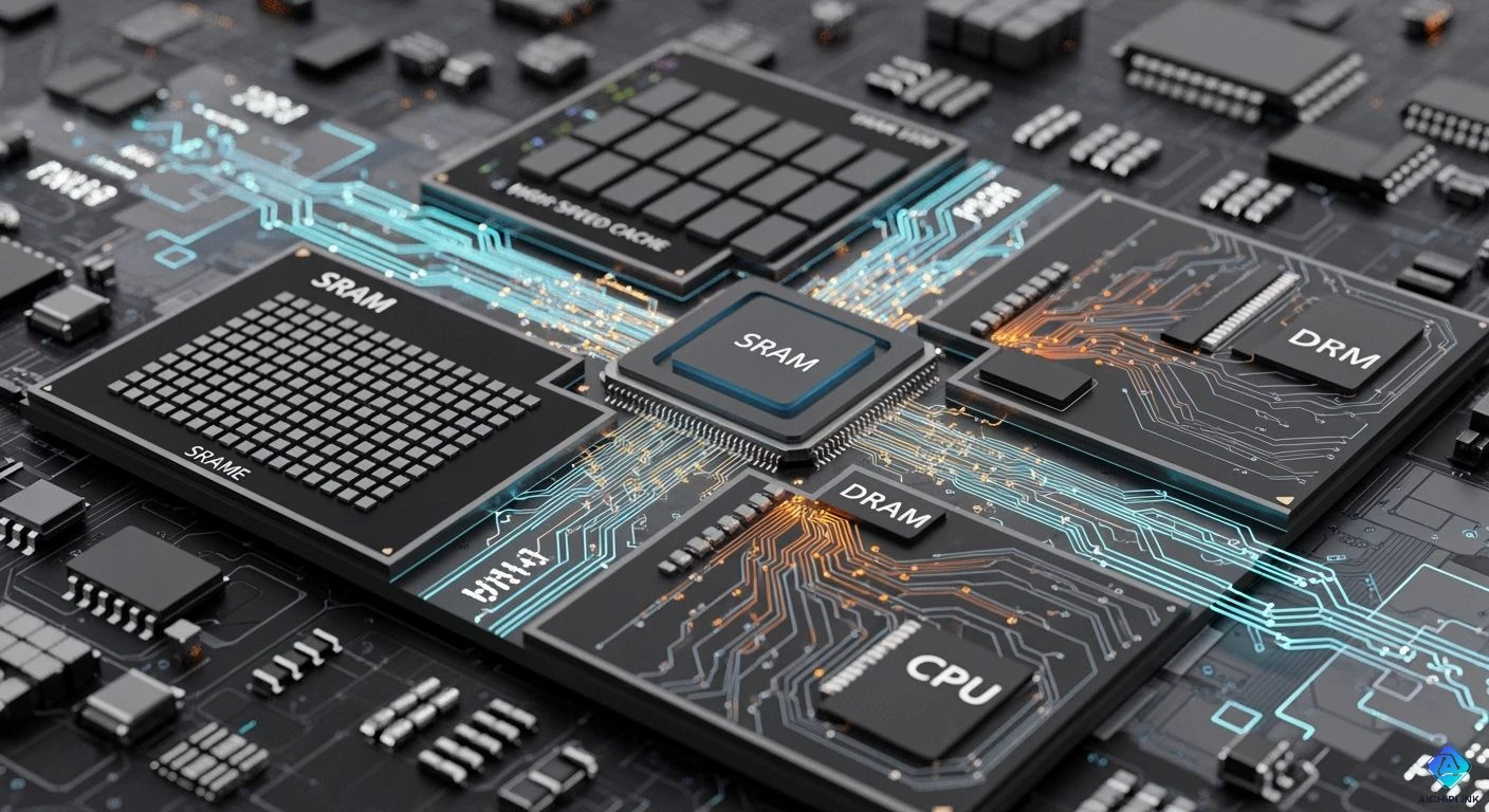
Modern phone chip designs balance two different hardware technologies to save battery power and improve speed. Static random-access memory offers super-fast access times and dependable performance. Modern processors use SRAM mainly for high-speed CPU cache systems. Dynamic random-access memory delivers unbeatable storage space at a much cheaper price per unit. Hardware designers place DRAM on a separate chip to act as the main system memory.
Choosing between SRAM vs DRAM forces a tough design decision. Putting fast SRAM directly on the main processor chip cuts down on data wait times. Using dense LPDDR DRAM on a separate chip stores big amounts of data efficiently. Working together, these memory levels deliver great overall speed and stretch total battery life.
Key Takeaways
-
SRAM gives processor cores extremely quick access to the data they are currently using.
-
DRAM provides a lot of storage space at a lower price for each piece of data.
-
SoC memory controllers balance both memory types to save battery life.
-
Hybrid memory systems mix fast response times with high data transfer performance.
SRAM Performance and Power Dynamics
SRAM Latency and Cache Efficiency
Modern microprocessors rely on static ram for memory tasks. A typical six-transistor sram cell uses two cross-coupled inverters to store data. This latch structure holds information securely without periodic refresh cycles. The direct design eliminates controller delay, shortens access time, and increases speed during active execution. Fast cache memory systems supply instant data to execution units, ensuring smooth computational flow.
-
Latch memory storage preserves data continuously while system power remains active.
-
Precharged bitlines and transistor switching deliver single-cycle operations.
-
Deterministic timing simplifies processor logic and boosts execution efficiency.
Engineers select sram for cpu cache designs because the memory technology operates much faster than dram. Close physical proximity to compute cores minimizes signal delay across the silicon chip. A Cortex-X2 processor core achieves an L2 cache hit latency under 4 ns. The same core records an L3 cache latency of 18.18 ns across larger memory arrays. This low latency capability allows execution units to retrieve instructions rapidly, sustaining peak processing speed.
Cell Area and Static Leakage Current
Physical size limits make it hard to fit lots of sram onto silicon chips. Each small bitcell requires six transistors, taking up significant room inside on-chip memory blocks. TSMC 5nm process technology achieves a densest sram bitcell area of 0.021 µm². Upgraded 3nm manufacturing processes like N3E maintain an identical sram bitcell area of 0.021 µm², showing clear scaling limits in sub-5nm nodes.
| Process Node | Bitcell Area |
|---|---|
| TSMC 5nm | 0.021 µm² |
| TSMC 3nm (N3E) | 0.021 µm² |
Because of these large footprints, chip makers cannot build huge sram main memory banks directly on processor dies. Advanced process nodes also lose extra power from static current leakage through tiny transistor gates. This wasted idle energy lowers total battery performance in low-power mobile systems. To fix this, hardware designers balance memory speed by linking small sram levels with separate off-chip memory parts. Smart sram setups protect overall battery life while keeping processing speeds very fast.
DRAM Density and Refresh Overhead
High Density DRAM Cell Design
Low-power system designs require high-density memory storage components. System architects select dynamic random-access memory to maximize capacity within tight silicon space constraints. Modern processors connect to external dram chips to store large software programs. High-density dram architectures pack millions of bit cells onto a small footprint. A typical dram cell uses one transistor and one capacitor. Advanced dram nodes like D1a and D1-beta tilt active islands at 69 degrees to the wordline. These compact LPDDR5 layouts yield a tiny dram cell size of 7.8F².
The simple cell structure creates unique operational behaviors during data retrieval.
-
The cell stores each bit as electric charge in a tiny capacitor.
-
The read operation depletes the charge, making reading destructive.
-
Sense amplifiers immediately apply a voltage to write data back by recharging the capacitor.
-
Immediate write-back steps prevent data loss caused by destructive read actions.
Dynamic Refresh Cycles and Latency
Capacitors lose charge over time. Therefore, dynamic ram arrays require constant management. A memory controller issues periodic refresh commands to restore charge inside dram circuits. These recurring updates affect overall memory efficiency.
| Parameter / concept | Typical LPDDR5 value | Meaning and effect on read latency |
|---|---|---|
| tREFI | 3.9 µs (3900 ns) | Refresh interval: how often a refresh command must be issued. |
| tRFC | ~200 ns | Refresh cycle time: while refresh is in progress, the DRAM is unavailable to serve reads/writes. |
| Refresh overhead | 200/(3900+200) ≈ 4.8% | Refresh consumes about 5% of bandwidth, making the memory unavailable for ~200 ns every 3.9 µs. |
| Latency mechanism | ~200 ns blocking every 3.9 µs | A read request arriving during a refresh window is delayed until refresh completes, so refresh can add up to ~200 ns of effective read latency. |
Periodic updates reduce available memory bandwidth while increasing data access time. Memory controllers balance refresh tasks to increase operational speed. Off-chip dram interfaces suspend bus transactions during refresh windows. A request arriving mid-cycle faces higher memory latency. Mobile processors adjust clock speed settings to maintain high transfer speed. Fast bus lines sustain execution speed while optimizing power efficiency across dense dram modules.
SRAM vs DRAM Architectural Comparison
Chip designers study memory options by checking key structural metrics. Every microchip layout balances raw speed against total physical space. Comparing sram vs dram structural features helps designers make smart hardware choices. This key sram vs dram trade-off shapes modern mobile processor designs.
Latency and Throughput Metrics
The design difference between static ram and dynamic ram directly impacts overall system speed. Small internal caches using sram achieve extremely low latency performance. A CPU core fetches data from an L2 cache in under 4 ns. In contrast, off-chip dynamic random-access memory takes a much longer access time. Requests to main memory face higher latency because controller steps and command sequences add big delays.
| Architecture Metric | SRAM Cache | LPDDR5 DRAM |
|---|---|---|
| Primary Design Focus | Minimal Access Latency | Maximum Storage Capacity |
| Typical Access Latency | Under 4 ns (L2 Cache) | Exceeds 50 ns (Main Memory) |
| Bandwidth Delivery | Localized High Speed | Massive Bus Bandwidth Transfers |
| Circuit Mechanism | Transistor Flip-Flop Latch | Charged Capacitor Array |
Cache systems provide localized high speed to keep processor tasks running at top speed. However, system-wide data moves demand huge bus capacity. Modern mobile chips solve this latency vs bandwidth trade-off by placing both memory types in one system. The main sram cache gives instant access to active instructions. Meanwhile, the primary dram bank delivers steady data streams over multi-channel paths. This layout boosts total bandwidth while hiding memory lag during heavy work.
Engineers know that sram stays much faster than dram during real-time computing tasks. The static memory latch changes bit lines without delay. A dynamic cell setup must open rows, charge bitlines, and run regular refresh commands. These extra steps slow down transfer speeds during continuous read actions in dram banks. The memory controller manages both levels to maintain steady system power. Fast cache layers handle quick requests, while dense external memory channels maintain high overall bandwidth across programs.
Cost per Bit and Area Footprint
Silicon manufacturing limits decide total chip space allocation. A standard sram bitcell needs six separate transistors, taking up major silicon area. Modern TSMC 5nm process technology creates an sram bitcell area of 0.021 µm². Upgraded TSMC N3E node technology makes the same sram bitcell area of 0.021 µm², showing clear scaling limits in new nodes. These large bitcell sizes raise production cost per bit on main processor chips.
External dram chips offer far greater storage density inside mobile devices. A typical dynamic cell packs one transistor and one capacitor into a tiny 7.8F² layout. This high-density setup greatly lowers production cost per bit for dram main memory. System architects cannot build huge on-chip sram structures without raising chip manufacturing costs to unmanageable levels.
Modern System-on-Chip designs use hybrid memory levels to balance total system speed with total production expense. Factories save expensive on-chip space only for critical cache systems. External chip makers produce cheap LPDDR5 dram chips on separate dedicated dram wafers. This physical split maximizes total storage space while lowering total system cost. The design separation lets mobile processors reach peak computing speed while keeping product prices affordable.
System Integration in Low Power SoCs
Hybrid Memory Hierarchy Design
Today's phone chips blend small internal sram caches with separate lpddr dram main arrays. These power-saving systems process heavy data streams for high-performance apps. Super-fast sram blocks keep key data right next to the processor cores for instant access. This layout speeds up information retrieval. Meanwhile, large external dram chips hold big system files, game graphics, and program data.
This mixed setup balances top processing speed with total battery power efficiency. On-chip sram layers answer most data requests directly inside the processor. Catching data early prevents costly requests to the main memory chip. As a result, the chip saves energy by avoiding long data transfers across circuit boards. Multi-channel LPDDR5 setups use 16 separate memory banks to supply high bandwidth during heavy tasks. Fast cache blocks manage local data traffic, keeping processing cores supplied with data.
Chip designers arrange memory levels to stop data from traveling long distances. Local caches answer small data requests right away. When cores need large files, the controller pulls big data blocks from main storage. The multi-tiered cache system predicts needed data and pre-loads it early. This organized layout keeps processors running smoothly without overheating the device.
SoC Memory Controller Power Optimization
Memory controllers guide data transfers between processor cores and main storage chips. Smart internal logic saves power by using sram caches to limit external dram access. Controllers also switch between special power modes to manage total energy use. Active dram chips use 500 to 800 mW of power. Idle modes cut usage to 50 mW. Regular self-refresh uses 5 to 15 mW. Partial refresh drops power to 2 to 8 mW. Deep power-down uses under 1 mW.
Controllers lower dram clock speeds and working voltages during quiet moments. The system drops core and interface power from 1.05V and 0.5V down to 0.9V and 0.3V. Slower speeds save significant battery life during basic tasks. Controllers use Data Bus Inversion to stop memory lines from constantly switching signals. They also send Write X commands to fill memory space without flipping data wires.
Smart hardware logic groups memory commands together to prevent extra energy waste. Organizing read and write tasks lets memory channels stay in low-power modes much longer. Controllers hold off on background tasks until they become necessary. Additionally, memory banks can go to sleep independently while active blocks keep working. This targeted power control cuts overall energy use during light daily tasks.
-
The sram layer delivers maximum speed for local chip operations.
-
The dram storage provides huge capacity for large data files.
-
Smart hardware controllers balance sram speed and dram bandwidth for peak performance.
-
On-chip sram caches save bus bandwidth while smart power controls protect battery life.
Phone chips use both sram and dram together to reach top processing speeds. Internal sram stores help the processor grab active data fast, boosting overall work speed. At the same time, thick lpddr dram chips give huge storage room for main system files. This mixed memory layout delivers fast performance while saving full battery power.
| Technology | Read Latency | Write Latency |
|---|---|---|
| ReRAM | 10-100 ns | 50-500 ns |
New memory inventions like MRAM and ReRAM fill the gap between small storage size and permanent data speed. These smart circuit layouts mix tiny bit storage with low idle power waste. As a result, future memory setups will rely less on older sram and outer dram parts.

Written by Jack Elliott from AIChipLink.
AIChipLink, one of the fastest-growing global independent electronic components distributors in the world, offers millions of products from thousands of manufacturers, and many of our in-stock parts is available to ship same day.
We mainly source and distribute integrated circuit (IC) products of brands such as Broadcom, Microchip, Texas Instruments, Infineon, NXP, Analog Devices, Qualcomm, Intel, etc., which are widely used in communication & network, telecom, industrial control, new energy and automotive electronics.
Empowered by AI, Linked to the Future. Get started on AIChipLink and submit your RFQ online today!
Frequently Asked Questions
Why do processor cores rely on sram for cpu cache designs?
Processors choose sram for cache blocks because static memory runs faster than dram. Transistor latches hold data constantly without needing regular refresh cycles. This simple design cuts down data wait times, helping processing units fetch active instructions quickly.
How do sram vs dram systems balance memory bandwidth?
Internal sram blocks send data to nearby cores immediately. Meanwhile, outer lpddr dram channels supply heavy system bandwidth through 16 separate memory banks. The controller blends both parts together, offering high overall bandwidth while keeping processing delays low and clock speeds fast.
How does dynamic memory prevent data loss during chip operations?
A dynamic cell holds data as an electric charge inside one small capacitor. Capacitors leak this electric charge all the time. To fix this, a built-in memory controller sends regular refresh commands every 3.9 µs to recharge the full memory grid, keeping system data safe.
How do smart controllers save energy during main storage transfers?
Controllers direct main data requests to local sram cache blocks first. Catching data on the chip cuts down on extra visits to the outer dram memory. This system saves total memory bandwidth, drops operating voltages, and extends battery life during light daily tasks.
Can non-volatile technologies match sram speed in mobile processors?
Newer non-volatile options like ReRAM offer quick read times. Even so, writing data still takes extra time to finish. Modern low-power chips still need sram caches to run at top speed, while non-volatile circuits broaden future built-in memory choices.