How is an FPGA programmed?
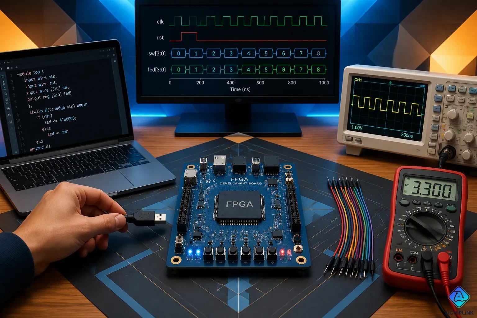
How is an FPGA programmed? You program an FPGA by loading a configuration bitstream. This binary file sets how the chip's internal logic blocks and interconnects work. Unlike a CPU, no instruction sequence runs here. Instead, you customize the hardware itself. The field programmable gate array market shows this growing demand, with a projected compound annual growth rate of 9.25% from 2025 to 2030. The process moves through five stages: design entry, synthesis, implementation, bitstream generation, and device configuration. Each step turns your idea into working hardware. This guide walks you through every stage in plain language. You will see how FPGA programming turns code into a customized circuit.
Key Takeaways
-
FPGA programming creates hardware, not software. You build circuits, not instruction sequences.
-
The process includes five stages: design entry, synthesis, implementation, bitstream generation, and device configuration.
-
You can reprogram an FPGA anytime. This lets you fix bugs or add features after deployment.
-
Beginners can start with an easy project like an LED blinker. Free tools and beginner boards make it simple.
-
A bitstream is very important. It sets up every logic block and wire inside the chip.
How is an FPGA programmed? Starting with Design Entry
You start FPGA programming by describing a digital circuit. This step is not about writing software. You define how logic gates connect, how signals flow, and how the circuit acts over time. Think of it as drawing a blueprint for hardware. The FPGA design tools you use will later turn this blueprint into a working configuration.
Writing HDL in Verilog or VHDL
Most designers describe circuits with a hardware description language (HDL). Verilog and VHDL are the two most common choices. Each language lets you define modules, signals, and timing behavior. Your choice affects how fast you learn and how easily you spot mistakes.
| Aspect | Verilog | VHDL |
|---|---|---|
| Learning Curve | Easier for beginners, especially from programming backgrounds | Steeper initial curve but encourages good design practices |
| Simulation & Debugging | Permissive, may hide errors until later stages | Strict typing catches mistakes early, but increases coding time |
| Ease of Learning | C-like syntax, easier for those with programming background | Verbose, strong typing, more structured but harder initially |
| Design Complexity | Simpler constructs, suitable for smaller projects | Strong typing and concurrent design support large projects |
Verilog gives you an easier start. Its C-like syntax feels familiar if you have coded before. This familiarity makes it less scary for beginners. VHDL takes more effort at the beginning. Its strict typing catches errors early. That discipline helps on big projects. Beginners often start small, so Verilog appeals to them first. VHDL's strict rules can be too much for newcomers. Both languages work well for any FPGA. Pick one and practice it regularly.
High-Level Synthesis as an Option
High-level synthesis (HLS) lets you use C or C++-like code as a starting point. You describe behavior at a higher level. The tool then creates hardware. This approach speeds up development for complex algorithms. However, HLS comes with trade-offs.
| Trade-off Category | Reported Performance Trade-off |
|---|---|
| Hardware optimization | HLS may produce less optimized hardware than hand-crafted HDL unless carefully refined iteratively. |
| Hardware insight requirement | Optimal performance still demands deep hardware knowledge, as HLS tools may not generate the most optimized structures. |
| Abstraction vs. control | Abstraction obscures hardware intricacies, making FPGA-specific optimization harder; fine-grained HDL control may be needed for performance-critical designs. |
| Efficiency vs. manual coding | HLS may not match the efficiency of manual HDL coding, and debugging generated code can be difficult. |
| Resource/performance/power overhead | Higher abstraction and automation can introduce overhead and inefficiencies in resource utilization, performance, or power consumption. |
| Resource utilization & synthesis | HLS may lead to suboptimal resource utilization, longer synthesis times, and limited support for complex designs. |
HLS works best for quick prototyping. You gain speed but lose fine control. Hand-coded HDL still wins for performance-critical FPGA designs. Many teams mix both methods. They use HLS for early exploration and HDL for final optimization. This mixed approach balances speed and efficiency.
Synthesis Turns HDL into a Netlist
Synthesis is the step where your HDL code becomes a gate-level netlist. This netlist describes logic blocks and the connections between them. Your fpga design tools read your code, check it, and build this structure. Think of synthesis as translating your blueprint into a detailed parts list.
What Synthesis Does
The synthesis tool reads your Verilog or VHDL code and checks the syntax first. It looks for errors like missing semicolons or mismatched signal names. Then it infers hardware from your behavioral descriptions. For example, when you write a clocked process with a memory array, the tool recognizes a RAM template. It maps that code to a block RAM inside the fpga.
The tool also reports warnings. A warning might tell you that it inferred a latch instead of a flip-flop. You should read these messages carefully. They often point to bugs in your code. Fixing warnings early saves time later.
Reading Synthesis Output
After synthesis finishes, you get a report. This report shows quality metrics for your design. You can use these numbers to judge whether your fpga design meets its goals.
| Metric | Value |
|---|---|
| Total cell area | 45,234 µm² |
| Cell count | 12,456 cells |
| Sequential cells | 2,345 (18.8%) |
| Combinational cells | 10,111 (81.2%) |
| Critical path delay | 1.85 ns |
| Clock period | 2.0 ns |
| Slack | 0.15 ns (MET) |
| Number of failing paths | 0 |
| Leakage power | 2.5 mW |
| Dynamic power | 485 mW |
| Total power | 487.5 mW |
| Clock network power | 145 mW (29.8%) |
A positive slack of 0.15 ns means your fpga timing passes. Zero failing paths confirm this. The cell count tells you how much logic your fpga uses. High combinational cell counts may signal that you need to pipeline your design. Power numbers help you plan your thermal budget. Review these metrics before you move to implementation.
Implementation Maps the Design onto FPGA Resources
Implementation takes your netlist and picks where each logic block goes inside the fpga. It also selects which wires link those blocks. This stage turns a general parts list into a real physical layout. Your fpga design tools do this work on their own, but you guide them with constraints.
Placement and Routing
Placement puts every logic cell at a certain spot on the chip. Routing then draws the links between those cells. The tool tries to keep wire length short and avoid crowding. A good placement makes routing simpler. A bad placement pushes signals through long, packed paths.
Higher clock speed goals make this job tougher. Faster clocks squeeze the time for logic to settle. Multi-level logic functions then break setup time rules more often. These breaks create critical timing paths. The placement engine must work harder to find the best spots. Build times get longer, and timing results become less steady. Fixed blocks like memory and DSP slices limit routing options even more. You can add pipeline registers between them to cut physical distance and routing congestion. That change boosts the success rate of place-and-route at high clock speeds.
Timing Analysis and Constraints
Timing constraints tell the tools what performance you need. You set clock periods, input delays, and output requirements. The tools then aim their optimization at critical paths. Without constraints, the software guesses your goals. With them, timing closure becomes a focused effort.
Higher clock speeds need more complex constraints and multi-corner timing analysis. At advanced process nodes, interconnect delays take over. Placement becomes key to avoid long routing paths while stopping congestion. Your constraints directly push synthesis and place-and-route tools toward the paths that matter most. This focus decides whether your fpga reaches timing closure and successful routing. Check your timing reports after each run. Change constraints when paths fail. Each round brings your fpga closer to its target frequency.
Generating the Configuration Bitstream
After implementation is done, you need a binary file that tells the chip exactly how to set itself up. This file is called the bitstream. It defines every logic block setting and every interconnect switch inside the device. Think of it as the final set of instructions for the hardware you built.
From Netlist to Bitstream
Your fpga design tools turn the placed and routed netlist into a binary bitstream through a clear step-by-step process. First, static timing analysis checks if signals can travel within one clock period. If timing violations exist, you must fix the design or relax the clock. Once timing passes, the tools create the bitstream binary that sets up every LUT, flip-flop, and routing switch.
Modern tools also add safety features into this file. Watchdog timers and parity checks help spot fault injection attacks and keep configuration safe. Error detection and correction codes (ECC) find and fix errors, protecting data during configuration and operation. Bitstream compression shrinks the configuration bitstream size stored in external memory, which speeds up download over the configuration interface before the device decompresses the data during configuration.
Security matters too. Bitstream encryption stops unauthorized access, cloning, hardware Trojan insertions, reverse engineering, and tampering. Modern devices support AES encryption to defend against passive attacks.
An attacker could copy bitstreams through a Man-in-the-Middle (MiM) attack and sell them at a lower price to different cloud service providers. This not only cuts the original provider's profits and market share but also hurts their reputation.
Common Bitstream Formats
Bitstream formats differ by vendor. Each company uses its own file extensions for SRAM configuration, flash storage, and portable programming.
| Vendor | SRAM Configuration | Flash/Non-Volatile | Additional Portable Formats |
|---|---|---|---|
| Xilinx/AMD | .bit | .mcs, .bin | .svf, .jam/.stapl |
| Intel/Altera | .sof | .pof, .jic | .svf, .jam/.stapl |
| Lattice | .bit | .jed | .svf, .jam/.stapl |
The bitstream is what actually programs the fpga. Without it, your design stays as abstract code. With it, the fpga becomes the circuit you described.
Loading the Bitstream onto the FPGA
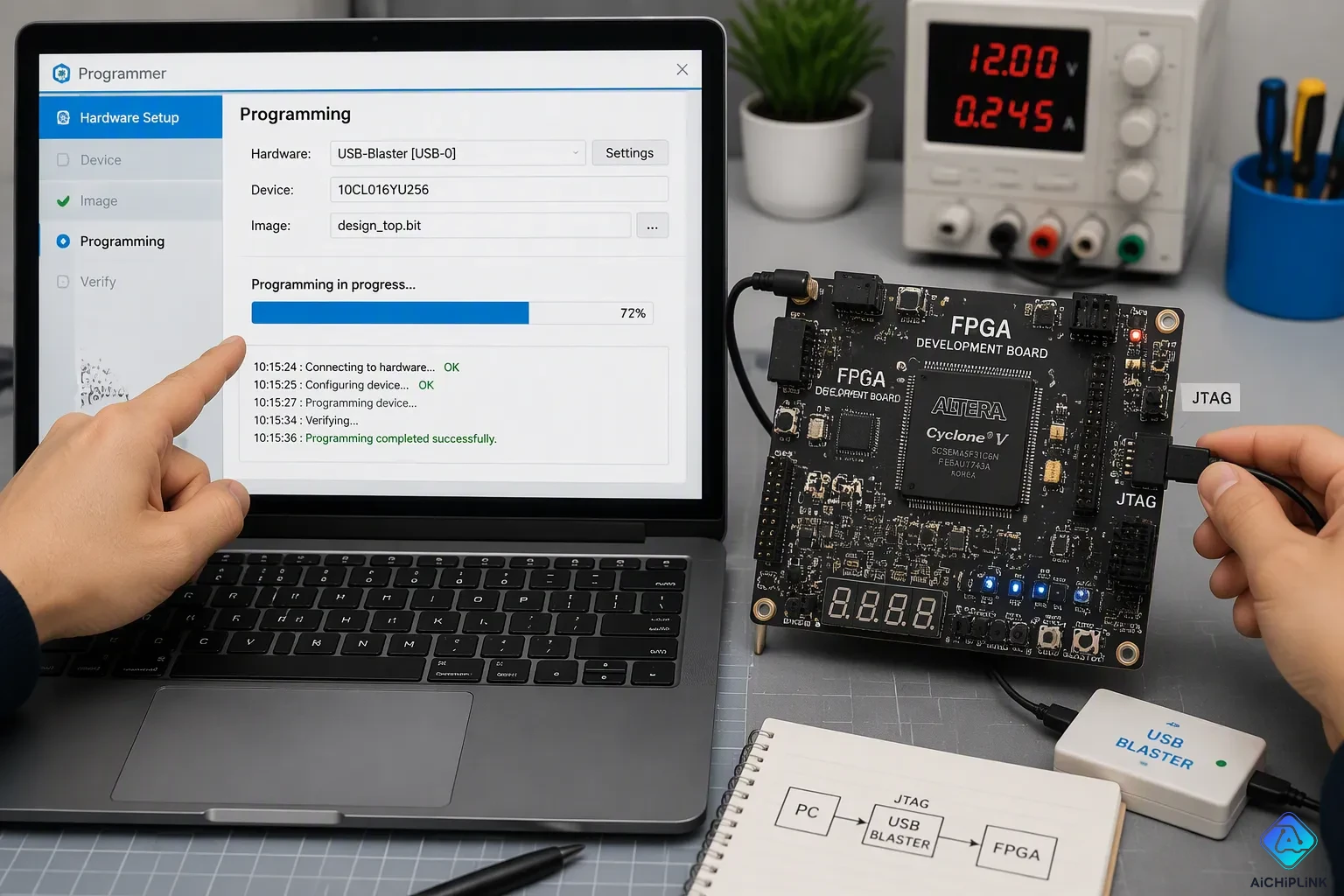
You have a bitstream file ready. Now you need to put it into the device. This last step makes your design work. You have two main ways: direct setup using JTAG or automatic loading from flash memory.
JTAG and Direct Configuration
JTAG is the usual way to set up the chip directly and temporarily during development. You plug a cable from your computer to the fpga board. The software sends the bitstream through the Test Access Port, a four-wire connection. The device sets itself up and begins running your design. This setup only works while power stays on. Turn the power off and on, and the fpga forgets everything. You have to load the bitstream again each time.
JTAG also supports boundary scan testing, which helps you fix problems in your setup. Boundary scan cells sit at the device edge between the core and the pins. In test mode, these cells separate the core from the pins. Each pin can then be driven or read on its own. This method lets you find devices and check for open or short circuits even when only power, ground, and one JTAG-chain device are available. You can find assembly defects like missing parts, solder problems, and stuck faults. A golden test helps you rule out bad hardware and focus on fixing firmware. Production test and repair stations also use this method to load images and run checks.
Watch out for configuration pins that might float. Pins like INIT_B and PROG_B can cause test failures if pull-up or pull-down settings are wrong. Adding proper pull-downs, like on HSWAP, makes boundary-scan more reliable.
How fast data moves depends on your programming method. The table below shows typical speeds.
| Programming Method | Data Transfer Speed |
|---|---|
| Traditional JTAG (serial shift through JTAG chain) | 20 MHz TCK (typical max) |
| FPGA-based flash programming | 55 MHz TCK (FPGA max supported) |
| XJFlash with Everspin PERSYST xSPI STT-MRAM | 32 Mbit/s sustained |
| XJTAG controllers (XJLink2, XJLink-PF40) | up to 166 MHz TCK, potentially over 100 Mb/s |
Flash Memory and Boot Loading
Flash memory lets the fpga load its setup automatically when power turns on. You save the bitstream in a flash chip on the board that keeps data without power. When power comes up, the device reads the bitstream from flash and sets itself up. No computer or cable is needed. This method works well for systems in the field where you cannot connect a programmer.
The boot process goes through a set order. The device detects power, turns off its internal reset, and starts reading configuration data. It loads the bitstream into its setup memory. When loading finishes, the device goes into user mode and runs your design.
FPGAs can be reprogrammed, so you can change the bitstream anytime. You might fix a bug, add a feature, or switch to a totally different circuit. Erase the flash, write the new bitstream, and restart. The device becomes something else. This flexibility is the main benefit of fpga technology. You are never stuck with one hardware design.
You have now seen the full pipeline. Design entry starts the process. Synthesis turns your code into a netlist. Implementation places and routes the logic. Bitstream generation creates the configuration file. Device loading makes it all work. This flow answers how is an fpga programmed? directly. Remember, fpga programming defines hardware, not software. You build circuits, not instruction sequences. Try a simple project on a beginner board. A basic LED blinker works well. See each stage in action. Watch your code become a working physical circuit. The process becomes intuitive after just one or two complete runs. You will gain confidence quickly. Each new project gets easier.

Written by Jack Elliott from AIChipLink.
AIChipLink, one of the fastest-growing global independent electronic components distributors in the world, offers millions of products from thousands of manufacturers, and many of our in-stock parts is available to ship same day.
We mainly source and distribute integrated circuit (IC) products of brands such as Broadcom, Microchip, Texas Instruments, Infineon, NXP, Analog Devices, Qualcomm, Intel, etc., which are widely used in communication & network, telecom, industrial control, new energy and automotive electronics.
Empowered by AI, Linked to the Future. Get started on AIChipLink and submit your RFQ online today!
Frequently Asked Questions
Does an FPGA run software like a computer?
No. A computer runs a list of instructions one after another. An FPGA configures its own hardware to act as the circuit you designed. You build logic paths, not a program. This is the core difference between FPGA technology and a standard processor.
Can you reprogram an FPGA after it ships?
Yes. You can erase the old bitstream and load a new one at any time. The device then becomes a different circuit. This flexibility lets you fix bugs, add features, or change the hardware's purpose long after deployment.
Do you always need a bitstream to use an FPGA?
Yes. The bitstream is the binary file that sets every logic block and wire inside the chip. Without it, the device stays blank. Your design code alone does nothing until the bitstream loads.
What tools do beginners need to start?
You need a hardware description language like Verilog or VHDL, a synthesis and implementation toolchain, and a beginner board. Most vendors offer free starter software. A simple LED blinker project teaches you how is an FPGA programmed from start to finish.