Emerging Storage Technologies: MRAM, RRAM, and PCRAM

Your processor waits billions of cycles while storage catches up. DRAM loses data when power disappears, and NAND flash writes slowly with limited endurance. These limits create a bottleneck you cannot ignore.
Emerging storage technologies offer a way forward. MRAM, RRAM, and PCRAM are next-gen memory types that keep data without power. These non-volatile memory options promise faster speeds and better durability than current ones.
You need to know these memory technologies because they will change computing. This article explains how each works, what makes them special, and where they fit. You will learn why data storage needs new ideas and how these options solve real problems. The future of memory starts here.
Key Takeaways
-
MRAM gives the quickest speed and the most write cycles, so it works best for cache memory.
-
RRAM offers high density and low power use, making it a good fit for storage-class memory.
-
PCRAM balances performance and cost, serving as persistent memory for databases and AI.
-
Each technology fills a specific gap in the memory hierarchy, working alongside DRAM and NAND flash.
-
These new memory types will make AI work faster, make devices last longer, and open up fresh ways to compute.
Emerging Storage Technologies: An Overview
The Need for New Memory Solutions
Your computer faces a growing problem. Processors get faster every year, but memory cannot keep up. This gap has a name: the memory wall. Modern workloads show the impact clearly. Matrix multiply operations use only 1-10% of theoretical peak FLOPS. Moving data costs about 1000 times more energy than a single 32-bit multiply. When data movement takes 80% of execution time, Amdahl's law limits speedup to just 1.25 times.
The numbers get worse with AI workloads. A 100B model with 10 million daily users would need 250 PB of SSD storage daily just for KV cache retention. Current memory hierarchies fail here. The "HBM → CPU DRAM → SSD" three-tier offloading approach relies on slow PCIe links and CPU involvement, creating a storage bottleneck. DRAM lacks the density for AI-scale demands. NAND flash suffers endurance limits and cannot meet throughput requirements. These emerging storage technologies address exactly these pain points.
Key Metrics for Comparing Memory Types
You need a framework to evaluate these new options. Three metrics matter most.
| Metric | What It Measures | Why It Matters |
|---|---|---|
| Latency | Time to read or write data | Determines how fast applications respond |
| Endurance | Number of write cycles before failure | Affects long-term reliability and cost |
| Density | Data stored per unit area | Drives cost per gigabyte and system capacity |
Latency tells you how quickly a system responds to requests. DRAM delivers nanosecond speeds but loses data without power. NAND flash retains data but writes slowly. Endurance measures write cycles. NAND flash degrades after thousands of writes. Density determines how much data fits in a given space. AI systems need several times more capacity than conventional servers. DRAM shortages persist through 2026 because of this demand.
These emerging memory technologies aim to combine the best traits. They offer non-volatile memory with better speed than flash and better density than DRAM. The next sections examine each technology in detail. You will see how MRAM, RRAM, and PCRAM tackle these challenges differently. Each of these emerging storage technologies brings unique strengths. Together, they form a new class of non-volatile memories that could reshape computing.
MRAM: Magnetic Storage Basics
How MRAM Uses Magnetic States
Magnetic random access memory stores data using magnetism instead of electrical charge. This magnetoresistive ram technology relies on tiny magnets that point in one of two directions. Each direction represents a binary value: zero or one. This approach gives you non-volatile storage, meaning data survives power loss.
The core of each magnetic ram cell is a Magnetic Tunnel Junction, or MTJ. This structure has three layers: a reference layer with fixed magnetization, a thin tunnel barrier, and a free layer that can switch. The Tunnel Magnetoresistance effect creates the physical mechanism for storing data. When the two magnetic layers align parallel, electrons tunnel easily through the barrier, producing low resistance. When they align antiparallel, electron tunneling slows dramatically, producing high resistance. This resistance difference maps directly to binary data: low equals zero, high equals one.
Reading data from an MRAM cell is straightforward. You apply a small current and measure the voltage across the MTJ. The resistance value reveals the stored bit without disturbing it. This non-destructive readout makes MRAM efficient for frequent access.
Writing data requires more effort. Spin-transfer torque MRAM uses a transistor paired with the MTJ. You pass a spin-polarized current through the junction, and the electron spin transfers torque to the free layer. This torque flips the magnetization direction, aligning it parallel or antiparallel to the fixed layer. The write operation completes quickly, giving you speed comparable to DRAM.
MRAM Advantages and Current Challenges
MRAM offers impressive benefits. Its speed rivals DRAM while providing persistence like flash storage. Endurance is another strength; you can write to MRAM cells millions of times without degradation. This reliability makes it attractive for applications that demand frequent updates.
However, scaling MRAM to high densities presents real obstacles. The thermal stability factor determines retention time, and retention scales with the exponential of this factor. Smaller cells reduce the energy barrier, risking data corruption at high temperatures. This creates a direct conflict between density and reliability.
Write current density poses another problem. As cells shrink, the required current density exceeds one million amperes per square centimeter. This high current causes power inefficiency and can stress the interconnects through electromigration. Manufacturing variability also hurts yields. Variations in MTJ stack thickness and barrier uniformity create inconsistent switching voltages across the chip.
Peripheral circuits add further overhead. Specialized write drivers and sense amplifiers consume 30-40 percent additional silicon area compared to SRAM. This overhead reduces the effective density advantage you might expect. Despite these hurdles, MRAM continues to advance, with researchers exploring field-free switching and multi-pillar structures to overcome these limitations.
RRAM: Resistive Switching and ReRAM
The Mechanism of Filament Formation
Resistive random access memory, or RRAM/ReRAM, stores data by changing electrical resistance. Each cell has a metal-insulator-metal structure. When you apply voltage, the material switches between two resistance states. These states represent binary data.
The switching mechanism relies on conductive filaments. Here is how the process works:
-
An electric field makes oxygen ions move away from their spots, leaving oxygen vacancies that form a conductive filament.
-
This filament switches the cell to a low-resistance state (LRS), storing a logic '1'.
-
Reversing the field makes oxygen ions return, breaking the filament and switching the cell to a high-resistance state (HRS), storing a logic '0'.
The HRS to LRS switch is the 'set' process. The LRS to HRS switch is the 'reset' process. An external voltage pulse through the RRAM cell allows a transition from a high resistance state (HRS), or the OFF state usually called logic value '0', to a low resistance state (LRS), or the ON state—logic value '1' and vice versa. To read data from the RRAM cell, a small voltage that cannot change the current state determines whether the cell is in logic 0 (HRS) or logic 1 (LRS).
Materials matter for this process. Hafnium oxide (HfOx) shows resistive switching through oxygen vacancy filaments. Trap-assisted tunneling dominates electron conduction. Active electrodes like copper work for electrochemical metallization cells. Hafnium electrodes support the valence change mechanism. Binary oxides serve as the switching medium.
RRAM Benefits and Integration Hurdles
ReRAM offers impressive advantages over existing memory options. Nanosecond read and write speeds far exceed flash memory's microsecond operations. Write operations consume significantly less energy because RRAM operates at much lower voltages than flash. Read operations use less power. Standby power approaches zero since this memory requires no refresh cycles.
The simple two-terminal structure enables high density and scalability. Very small cell sizes become possible. Cross-point architectures without access devices could deliver ultra-high density. This resistive ram technology also compares favorably to other emerging options. RRAM operates faster than PCRAM. Its cell structure is simpler than MRAM's complex magnetic tunnel junctions.
However, integration hurdles remain significant. Cell-to-cell and cycle-to-cycle variations plague manufacturing. Stochastic filament formation creates inconsistent switching parameters. Endurance limits are still a concern. Sneak path currents in crossbar arrays require selector devices that increase complexity. Novel materials like hafnium oxide introduce contamination risks during CMOS fabrication. Variability increases at smaller nodes. Data retention degrades at elevated temperatures. These challenges affect the reliability of ReRAM products.
PCRAM: Phase-Change Memory Explained
How Chalcogenide Glasses Store Data
Phase change random access memory uses heat to switch a material between two states. The material inside each cell is chalcogenide glass, often Ge2Sb2Te5 or GST. This glass can exist in two forms. An amorphous state has atoms arranged randomly, creating high electrical resistance. A crystalline state has atoms in a regular pattern, creating low resistance. These two states represent binary data.
Here is how the switching works. A heating element, usually titanium nitride, sits below the glass. Electric current passes through the element and generates heat. To write a binary 0, the pcm system heats the glass above its melting point and then quickly cools it. This rapid quenching traps the atoms in a disordered amorphous structure. The high resistance state represents binary 0. To write a binary 1, the pcm system heats the glass to above its crystallization point, below its melting point. This allows the atoms to rearrange into a crystalline structure. The low resistance state represents binary 1. You can also create intermediate partially crystalline states. This lets a single cell store multiple bits, such as four distinct states for two bits per cell.
The switching mechanism relies on Joule heating. A brief high-current pulse melts the GST above its melting point, followed by abrupt quenching to trap the amorphous state. A longer lower-current pulse heats the material to above its crystallization point, allowing nucleation and grain growth to restore the crystalline state. This thermal cycling supports routine endurance of many cycles with data retention exceeding many years at standard operating temperatures.
PCRAM Performance and Scalability
PCM offers distinct advantages over flash memory. This memory operates at much lower voltages than NAND flash, which requires high voltages for programming. The phase-change mechanism also delivers faster write speeds. A Ta-GST device achieves a switching speed of a few nanoseconds with low energy consumption. Even ultra-thin films maintain long data retention at elevated temperatures, showing that thickness reduction trades off retention but improves speed and power. The reliability of pcm makes it suitable for applications that need persistent storage with frequent updates.
3D stacking represents the next frontier for phase-change memory. Intel has demonstrated 3D XPoint technology with few decks of cells. The company has revealed it can stack multiple decks. The explicit goal is to reduce costs by increasing the number of decks.
| Layer Count | Relative Cost | Scalability Status |
|---|---|---|
| Few decks | Baseline | Currently in production (Intel 3D XPoint) |
| More decks | Higher cost | Demonstrated by Intel, but cost-prohibitive for mass adoption |
| Many layers | Not cost-competitive | Not viable against existing technologies |
PCM cell area is smaller than MRAM, giving it a density advantage. PCM is also more mature than ReRAM, which is still not as far along despite being scalable. The next milestone for this memory is to stack more cells vertically and cram more bits per cell to compete with flash.
Comparing Emerging Storage Technologies
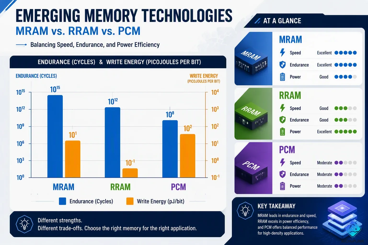
You now understand how each technology works. The next step is to see how they compare. These three emerging memory technologies serve different purposes. Each one balances speed, endurance, power, cost, and density in a unique way. No single option wins across all categories. Your choice depends on what you need most.
Speed, Endurance, and Power Trade-offs
The table below shows how MRAM, RRAM, and PCM stack up against each other on key performance metrics.
| Technology | Read Time | Write Time | Write Energy | Endurance |
|---|---|---|---|---|
| PCM | Very fast | Fast | Higher | High |
| STT-MRAM | Very fast | Very fast | Very low | Extremely high |
| RRAM | Very fast | Fast | Very low | Moderate to high |
MRAM leads in speed and endurance. Its write time is very fast, and its endurance is extremely high. This makes MRAM truly unlimited in practical terms. You can write to it many times without failure. Write energy per bit is very low, far lower than PCM's. RRAM matches MRAM read speed and comes close on write energy. However, RRAM endurance varies widely. This variability stems from the stochastic nature of filament formation. PCM offers the slowest write time. Its endurance still beats NAND flash by a wide margin.
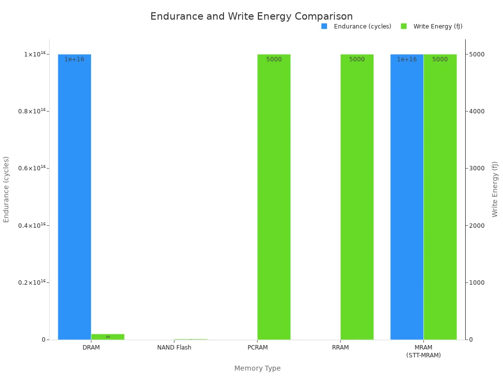
The chart above shows a clear pattern. MRAM and DRAM both offer very high endurance. NAND flash has much lower endurance. RRAM and PCM have moderate endurance. Write energy varies: DRAM and NAND flash have lower write energy, while the emerging memories have higher write energy. This is higher than DRAM and flash. However, these emerging storage technologies offer non-volatility. You gain persistence without the constant power drain of refresh cycles. System-level power savings can be significant.
Reliability also differs. MRAM offers very high endurance with lower power consumption than DRAM. RRAM has lower endurance than MRAM due to material fatigue. PCM underperforms DRAM in speed but still delivers fast enough performance for many applications.
Cost, Density, and Ideal Use Cases
Cost and density determine where each memory fits. MRAM has the smallest cell size potential but the highest manufacturing cost. Its complex magnetic tunnel junctions require precise fabrication. This makes MRAM expensive per gigabyte. You use MRAM where speed matters most. Cache memory in processors and embedded systems are ideal applications. MRAM can replace SRAM in some cases. It offers persistence without battery backup.
RRAM offers the best density potential. Its simple two-terminal structure scales to very small sizes. Cross-point architectures enable high-density storage without large transistors. This makes RRAM a strong candidate for storage class memory. You place storage class memory between DRAM and NAND flash in the hierarchy. It fills the gap with faster access than flash and lower cost than DRAM. RRAM also works well for neuromorphic computing. Its analog switching behavior mimics biological synapses. ReRAM variants continue to improve density through advanced materials research.
PCM strikes a balance. It offers better density than MRAM but lower cost. Its 3D stacking capability pushes density higher. PCM serves as persistent memory. You use it for applications that need fast non-volatile memory with high endurance. Database systems, AI inference, and enterprise storage benefit from phase-change memory. Intel's 3D XPoint technology demonstrated this use case.
Your choice depends on your priority. For maximum speed and endurance, choose MRAM. For the highest density and lowest cost, choose RRAM. For a balanced solution with good performance and moderate cost, choose PCM. These emerging memory technologies will coexist. Each one targets a specific layer in the memory hierarchy. Understanding their trade-offs helps you make the right decision for your next system.
Future Outlook for Emerging Memories
Streamlining MRAM Development
Making MRAM at scale needs exact work. The magnetic tunnel junction uses many film layers that must be placed with great care. The main magnesium oxide layer needs a nearly perfect crystal structure. Even one atom of height change can hurt how well it works. You see these problems when making more units.
Companies are fixing these issues now. TSMC puts MRAM into advanced FinFET processes at various nodes. This CMOS-friendly method cuts mask costs and development time. Wafer-level cost checks and yield tuning lower total ownership costs. Patent filings show more new ideas. A backside MRAM setup places cells on the opposite wafer side, removing metal layers in between. A T-shaped magnetic bottom electrode cuts parasitic resistance and stack height.
imec brings new breakthroughs in switching methods. Field-free switching for SOT-MRAM puts a ferromagnet in the hardmask, so no external magnetic fields are needed. This method keeps sub-nanosecond write speeds. A back-end-of-line compatible SOT device handles thermal budget limits. A deterministic VCMA write idea avoids pre-reading by using distinct threshold voltages. All devices show reliable high-frequency switching with very low write energy on 300mm infrastructure.
Streamlining RRAM Development
RRAM faces different problems. Endurance limits remain, and researchers still look for failure causes. Knowing these failures helps improve materials and manufacturing steps. Yield analysis offers a way forward. A two-stage method checks CMOS passivation etch openings first, achieving a significant yield. The second stage looks at full-device defects, giving a high yield for small arrays. Combined yield is moderate. Early R&D processes usually have low yield. Mature volume production achieves high yield.
Process-induced variations show up as systematic and measurable. Local device-to-device differences come from random filament formation. Automated optical inspection now matches manual analysis results. Common defects include connectivity loss between RRAM and CMOS layers.
Making these emerging memories profitably has always been a barrier to their wider adoption.
Your roadmap for streamlining mram and rram development depends on solving these manufacturing puzzles. The payoff extends beyond traditional storage. In-memory computing chips could leverage RRAM's analog switching for neuromorphic systems. MRAM could replace SRAM in embedded applications. These emerging storage technologies will mature through continued process refinement. Your next system may already benefit from these advances.
You now see the differences between these new storage technologies. MRAM gives the best speed and reliability. RRAM and ReRAM provide high density and use little power. PCM offers a good balance of performance and cost. No one technology is the best. Each one works best at a certain place in the memory stack. These new memory types will work together to fill spots that DRAM and NAND flash cannot. They will change how computers are built. You can expect AI tasks to run faster, devices to last longer, and new ways of computing. The future of storage looks bright. These new options give you choices you did not have before.

Written by Jack Elliott from AIChipLink.
AIChipLink, one of the fastest-growing global independent electronic components distributors in the world, offers millions of products from thousands of manufacturers, and many of our in-stock parts is available to ship same day.
We mainly source and distribute integrated circuit (IC) products of brands such as Broadcom, Microchip, Texas Instruments, Infineon, NXP, Analog Devices, Qualcomm, Intel, etc., which are widely used in communication & network, telecom, industrial control, new energy and automotive electronics.
Empowered by AI, Linked to the Future. Get started on AIChipLink and submit your RFQ online today!
Frequently Asked Questions
Which emerging memory technology offers the fastest performance?
MRAM is the speed leader. It writes data very quickly. It can handle a very high number of write cycles. This makes it great for cache memory. You get data saving without losing speed.
Will these technologies replace DRAM and NAND flash?
No, not completely. Each new memory type fills a certain need. One works well for cache. RRAM fits storage-class memory. PCM balances speed and cost. DRAM and NAND flash still serve other purposes.
How do you choose between these options?
Think about what matters most. Need top speed? Go with MRAM. Want high density at low cost? Pick RRAM or ReRAM. Looking for balanced performance? Choose PCM. Each memory type shines in different situations.
When will these technologies become mainstream?
Use is growing steadily. Manufacturing costs are still the biggest hurdle. As production increases, prices drop. You will see these options in more devices soon.