Introduction
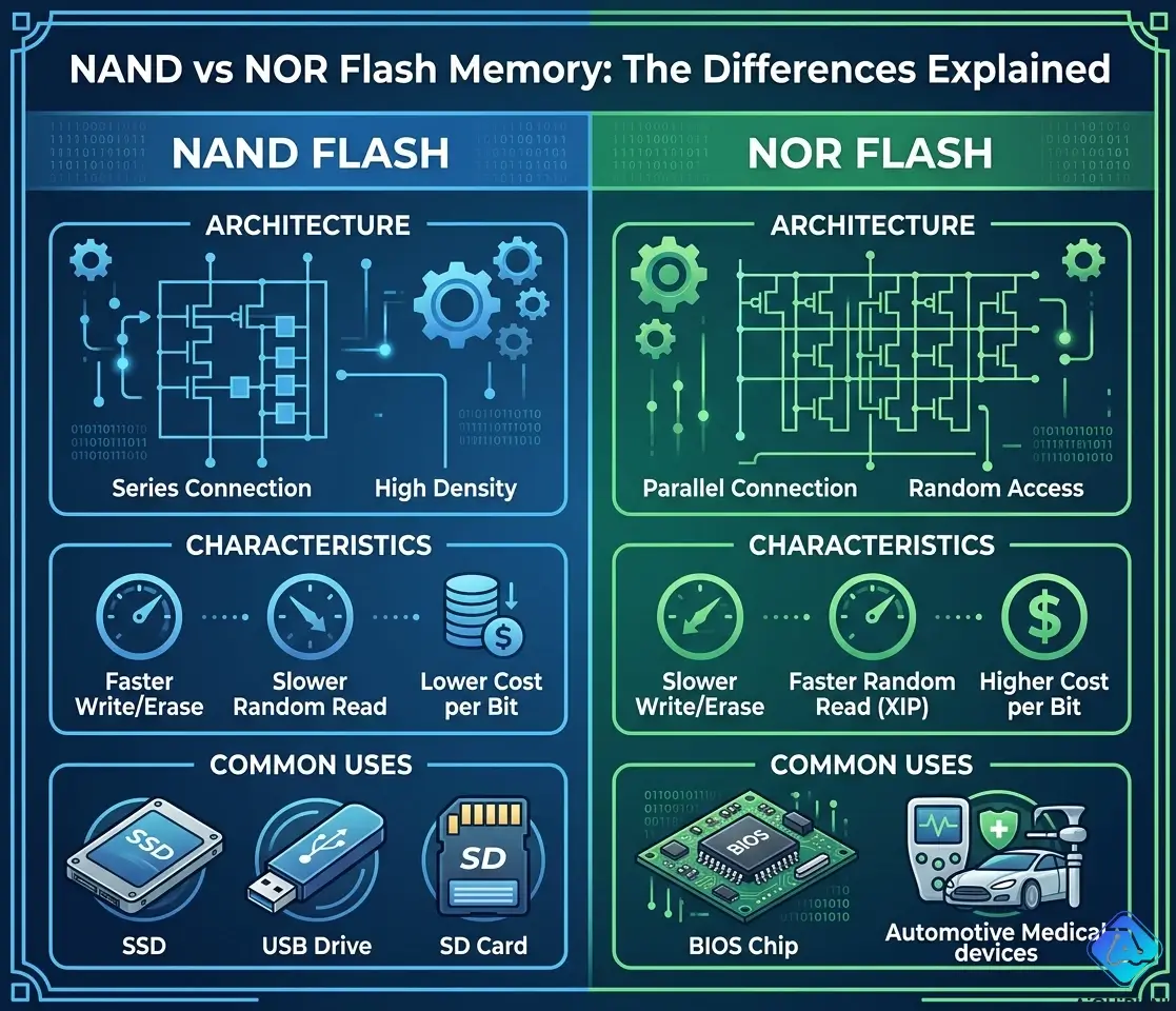
NAND and NOR flash are the two primary types of non-volatile memory used in modern electronics, each optimized for different use cases based on their fundamental architectural differences. While both store data without power, NOR flash excels at fast, random-access read operations making it ideal for code execution, whereas NAND flash prioritizes high storage density and fast sequential writes, making it perfect for mass data storage. This comprehensive comparison explains the key architectural differences between NAND and NOR flash, their performance characteristics, cost trade-offs, and which applications benefit most from each technology.
Overview & Basic Differences
What is Flash Memory?
Flash memory = Non-volatile storage technology that retains data without power, based on floating-gate transistors that trap electrical charge.
Two Main Types:
- NOR Flash (named after NOR logic gate architecture)
- NAND Flash (named after NAND logic gate architecture)
Quick Comparison Table
| Feature | NOR Flash | NAND Flash |
|---|---|---|
| Primary Use | Code storage & execution | Data storage |
| Read Speed | Fast random access (10-100 ns) | Slower random access (25-50 µs) |
| Write Speed | Slow (microseconds/byte) | Fast (page-based, ~200 µs) |
| Erase Speed | Slow (seconds/block) | Fast (milliseconds/block) |
| Density | Lower (fewer bits per chip) | Higher (4-10× more dense) |
| Cost per GB | $5-20 | $0.10-0.50 |
| Interface | Parallel (like RAM) | Serial (page-based) |
| Execute-in-Place | Yes (XIP) | No |
| Endurance | 100,000-1M cycles | 3,000-100,000 cycles |
| Typical Capacity | 1MB-256MB | 1GB-1TB+ |
Key Distinction
Memory Analogy:
- NOR Flash = Like a library with direct book access—you can grab any book instantly, but limited shelf space
- NAND Flash = Like a warehouse with pallet storage—massive capacity, but you need to pull entire pallets (pages) at once
Architecture Comparison
NOR Flash Architecture
Cell Organization:
Parallel connections (NOR gate logic):

           BL (Bit Line)
            |
    ┌───────┴───────┐
    │       │       │
   [Cell] [Cell] [Cell]  ← Each cell directly connected to bit line
    │       │       │
    └───────┬───────┘
           WL (Word Line)

Each cell = Floating-gate transistor
Connection = Parallel (like RAM addressing)
Key Architectural Features:
1. Random Access:
- Each memory cell individually addressable
- Direct connection to bit lines and word lines
- Similar to SRAM/DRAM addressing scheme
2. Execute-in-Place (XIP):
CPU → Address Bus → NOR Flash → Data Bus → CPU

CPU can directly execute code from NOR flash without copying to RAM
Access time: 10-100 ns (similar to RAM)
3. Bit-Level Access:
- Can read/write individual bytes
- No need for page/block operations (for reads)
4. Physical Layout:
- Larger cell size (lower density)
- More address/control circuitry
- Resembles conventional ROM layout
NAND Flash Architecture
Cell Organization:
Series connections (NAND gate logic):

    BL (Bit Line)
     |
   [Cell] ← Series connected cells
     |      (like Christmas lights)
   [Cell]
     |
   [Cell]
     |
   [Cell]
     |
    GND

Cells connected in series (NAND string)
Fewer connections = higher density
Key Architectural Features:
1. Page-Based Access:
Read/Write unit: Page (typically 2KB-16KB)
Erase unit: Block (64-256 pages)

Cannot access individual bytes directly
Must read entire page, modify, write back
2. High Density:
- Series connection = fewer contacts per cell
- Smaller cell size (4-5F² vs NOR's 10F², where F = feature size)
- 3D NAND: Stacks cells vertically (96-232 layers)
3. No Execute-in-Place:
Cannot directly execute code
Must copy code to RAM before execution

Boot sequence:
NOR/ROM → Loads bootloader → Copies NAND contents to RAM → Executes
4. Block-Oriented:
- Read: Page granularity (2-16KB)
- Write: Page granularity
- Erase: Block granularity (128KB-4MB)
Performance & Characteristics
Read Performance
NOR Flash:
Random Access Time: 10-100 ns (nanoseconds)
Sequential Read: 50-100 MB/s
Random Read: Excellent (no penalty)

Use case: Microcontroller fetching instructions
Access pattern: Random, byte-level
NAND Flash:
Page Access Time: 25-50 µs (microseconds) - first byte latency
Sequential Read: 200-500 MB/s (SLC), 1-3 GB/s (3D TLC/QLC)
Random Read: Poor (must read entire page)

Use case: SSD reading file
Access pattern: Sequential, page-level
Winner: NOR for random access, NAND for sequential throughput
Write Performance
NOR Flash:
Write Speed: ~10-100 KB/s (byte-by-byte)
Write Granularity: Byte-level
Write Process: Slow bit manipulation

Example: Writing 1MB takes ~10-100 seconds
NAND Flash:
Write Speed: 10-50 MB/s (page programming)
Write Granularity: Page-level (2-16KB)
Write Process: Fast page programming

Example: Writing 1MB takes ~20-100 milliseconds
Winner: NAND (10-100× faster for bulk writes)
Erase Performance
NOR Flash:
Erase Time: 0.5-5 seconds per block
Erase Block Size: 64-128KB
Total Erase: Very slow (minutes for entire chip)
NAND Flash:
Erase Time: 1-3 milliseconds per block
Erase Block Size: 128KB-4MB
Total Erase: Fast (seconds for entire chip)
Winner: NAND (100-1000× faster erase)
Endurance (Program/Erase Cycles)
NOR Flash:
Endurance: 100,000 - 1,000,000 cycles
Reason: Simpler cell structure, thicker oxide layer
Application: Code storage (infrequent updates)
NAND Flash:
SLC (Single-Level Cell): 50,000-100,000 cycles
MLC (Multi-Level Cell): 3,000-10,000 cycles
TLC (Triple-Level Cell): 1,000-3,000 cycles
QLC (Quad-Level Cell): 500-1,000 cycles

Reason: Higher bit density = thinner oxide = faster wear
Mitigation: Wear leveling, ECC (Error Correction Code)
Winner: NOR (10-100× higher endurance)
Density & Cost
NOR Flash:
Density: Low (difficult to scale beyond 256MB per chip)
Cost per GB: $5-20 (2024 pricing)
Reason: Larger cell size, parallel architecture

Typical use: 1MB-256MB applications
NAND Flash:
Density: High (1TB+ per chip possible with 3D NAND)
Cost per GB: $0.10-0.50 (2024 pricing)
Reason: Smaller cell size, series architecture, 3D stacking

Typical use: 8GB-2TB applications
Winner: NAND (10-100× lower cost per GB)
Applications & Use Cases
When to Use NOR Flash
1. Embedded Systems Boot Code
Application: Microcontroller firmware, BIOS/UEFI
Why NOR:
- Execute-in-Place (XIP): CPU runs code directly from flash
- Fast boot: No need to copy to RAM
- Random access: Jump to any instruction instantly
- High reliability: High endurance for code updates
Example:
MCU Boot Sequence (with NOR):
Power ON → CPU fetches reset vector from NOR (100 ns) → Executes bootloader

Total boot time: Microseconds
2. Small Code Storage (1MB-64MB)
Applications:
- Router firmware
- Network switch OS
- Automotive ECU code
- Industrial controller firmware
Why NOR:
- Small capacity needs (NOR cost-effective at <64MB)
- Code execution without RAM copy
- Byte-level updates possible
3. Critical Safety Systems
Applications:
- Automotive safety (ADAS, airbags)
- Medical devices
- Aerospace systems
Why NOR:
- High reliability (1M P/E cycles)
- Proven technology (mature, well-understood)
- Fail-safe: No complex controller needed
When to Use NAND Flash
1. Mass Data Storage
Applications:
- SSDs (Solid State Drives)
- SD cards, USB drives
- Smartphone storage
- Digital cameras
Why NAND:
- High capacity (128GB-2TB typical)
- Low cost per GB ($0.10-0.50)
- Fast sequential writes (100+ MB/s)
Example:
SSD Architecture:
[Controller] ← Manages wear leveling, ECC
     │
[NAND Flash Array] ← 256GB-2TB
     │
[DRAM Cache] ← Speeds up random access
2. eMMC/UFS Embedded Storage
Applications:
- Smartphones
- Tablets
- IoT devices
- Automotive infotainment
Why NAND:
- Integrated controller (eMMC/UFS packages)
- High density (8GB-512GB)
- Cost-effective for large storage
3. Write-Intensive Applications
Applications:
- Data logging
- Video recording
- Cache/buffer storage
- Temporary file systems
Why NAND:
- Fast write speed (10-50 MB/s)
- Fast erase (milliseconds)
- Acceptable for high write workloads (with wear leveling)
Hybrid Approaches
NOR + NAND Systems:
Common Architecture:
[NOR Flash] ← Boot code (1-16MB)
     │
    MCU/CPU
     │
[NAND Flash] ← Data storage (1GB+)
Use Cases:
- Embedded Linux systems
- Network appliances
- Industrial computers
- Automotive infotainment
Advantages:
- NOR: Fast, reliable boot
- NAND: Large, cost-effective data storage
- Best of both worlds
Technology Evolution
NOR Flash Trends
Status: Mature technology, declining market share
Current State:
- Stable at 45-65nm process nodes
- Limited capacity growth (max ~256MB practical)
- Focus on reliability, not density
- Niche applications (embedded systems)
Future:
- Gradual replacement by eMMC/UFS (with NAND inside)
- Still dominant in automotive, industrial
- Some designs moving to XIP-capable NAND variants
NAND Flash Trends
Status: Rapidly evolving, dominant flash technology
Key Developments:
1. 3D NAND (V-NAND):
Traditional NAND: Planar (2D)
3D NAND: Vertical stacking (96-232 layers)

Benefits:
- Higher density without scaling process node
- Better endurance than ultra-scaled planar
- Lower cost per GB
2. QLC (Quad-Level Cell):
SLC: 1 bit/cell (50K cycles)
MLC: 2 bits/cell (10K cycles)
TLC: 3 bits/cell (3K cycles)
QLC: 4 bits/cell (1K cycles)

Trade-off: Higher density, lower endurance
Solution: Aggressive wear leveling, large overprovisioning
3. Future: PLC (Penta-Level Cell, 5 bits/cell)
- Even higher density
- Even lower cost
- Challenging endurance (100-300 cycles)
Conclusion
NAND and NOR flash serve fundamentally different purposes based on their architectural trade-offs: NOR flash excels at fast, random-access code execution with high endurance making it ideal for firmware and bootloaders, while NAND flash dominates mass data storage with 10-100× higher density, faster sequential writes, and dramatically lower cost per gigabyte. Modern systems often use both—NOR for boot code, NAND for data—or increasingly adopt eMMC/UFS packages (NAND with integrated controllers) that provide managed storage for embedded applications.
Key Takeaways:
✅ NOR Flash: Fast random access, execute-in-place, high endurance, expensive
✅ NAND Flash: High density, low cost, fast sequential writes, page-based access
✅ NOR Use Cases: Firmware, bootloaders, small code storage (<256MB)
✅ NAND Use Cases: SSDs, SD cards, smartphones, mass storage (>1GB)
✅ Architecture: NOR parallel (RAM-like), NAND series (chain-like)
✅ Performance: NOR better random reads, NAND better sequential writes
✅ Cost: NAND 10-50× cheaper per GB
✅ Trend: NAND dominates (95%+ flash market), NOR niche but critical
Designing embedded systems or storage solutions? Visit AiChipLink.com for flash memory selection guidance, NAND/NOR sourcing, and system architecture consultation.

Written by Jack Elliott from AIChipLink.
AIChipLink, one of the fastest-growing global independent electronic components distributors in the world, offers millions of products from thousands of manufacturers, and many of our in-stock parts is available to ship same day.
We mainly source and distribute integrated circuit (IC) products of brands such as Broadcom, Microchip, Texas Instruments, Infineon, NXP, Analog Devices, Qualcomm, Intel, etc., which are widely used in communication & network, telecom, industrial control, new energy and automotive electronics.
Empowered by AI, Linked to the Future. Get started on AIChipLink.com and submit your RFQ online today!
Frequently Asked Questions
What is the main difference between NAND and NOR flash?
The key difference lies in architecture: NOR flash connects memory cells in parallel, enabling fast random access and execute-in-place (XIP), while NAND flash connects cells in series, achieving much higher density but requiring page-based access. As a result, NOR is ideal for firmware and code storage due to its low latency (10–100 ns), whereas NAND is better for bulk data storage thanks to its higher capacity, faster sequential writes, and significantly lower cost per GB.
Is NAND or NOR flash better for SSDs?
NAND flash is the only practical choice for SSDs because it offers high density, fast sequential read/write speeds, and low cost per gigabyte. NOR flash is unsuitable due to its low capacity, extremely high cost, and slow write performance. Modern SSDs rely on NAND combined with controllers, DRAM cache, and firmware to deliver high performance and reliability, making NAND the industry standard for all solid-state storage devices.
Can you use NAND flash for code execution?
NAND flash generally cannot execute code directly (no XIP) because it requires page-based access, has high initial read latency, and lacks byte-level addressing. Instead, systems copy code from NAND into RAM before execution—a method known as shadowing. In contrast, NOR flash supports direct execution, so many systems use a hybrid approach: NOR for boot code and NAND for operating systems and data.
Which flash type has better endurance?
NOR flash typically offers much higher endurance than NAND flash, with 100,000 to 1,000,000 program/erase cycles compared to NAND’s 500 to 100,000 cycles depending on cell type. NAND endurance varies widely—SLC being the most durable and QLC the least—while techniques like wear leveling and error correction help extend NAND lifespan. For applications requiring frequent rewrites, NOR or SLC NAND is preferred.
Why is NAND flash cheaper than NOR flash?
NAND flash is significantly cheaper due to higher density and more efficient manufacturing, achieved through smaller cell size, 3D stacking (dozens to hundreds of layers), and multi-level cell technology (TLC/QLC). In contrast, NOR’s parallel architecture limits scaling and increases silicon area per cell, resulting in much higher costs. This makes NAND dominant in mass storage, while NOR is reserved for low-capacity, high-reliability applications like firmware storage.