What is an SPI Flash Memory Interface and How It Works
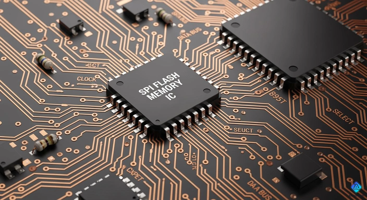
You can use an SPI flash interface. It provides fast storage. Your microcontroller keeps data safely. The system keeps data without power. This chip holds your important code. It uses a synchronous serial protocol. You read and write code easily. You can also erase firmware fast. The SPI bus uses four pins. These pins handle all data transfers. This saves space on your board. You get tiny, very reliable storage. It works using fast SPI lines.
Key Takeaways
-
SPI flash memory keeps your key data safe without power.
-
The SPI bus uses four simple wires.
-
These wires save board space.
-
Quad SPI speeds up data moves.
-
It moves four bits per clock tick.
-
Engineers use SPI flash memory for boot code.
-
This stores system code well.
Fundamentals of the SPI Flash Interface
You use the spi flash interface for data. It stores permanent system data. This non-volatile flash memory keeps data safe. It works without main system power. Your microcontroller needs this memory type. It helps steady long-term operations.
What is SPI Serial Flash Memory?
You transfer data fast. You use the serial peripheral interface standard. A solid-state drive uses flash technology. It holds binary data inside. It uses floating-gate transistors.
You pick hardware for your project. You must choose two primary architectures. NOR flash offers fast random reads. NAND flash handles bulk storage. It has rapid write cycles.
| Technical Dimension | NOR Memory | NAND Memory |
|---|---|---|
| Cell Connection | Parallel memory cell architecture | Series-connected cells in pages |
| Access Mode | Random access for words; supports Execute-in-Place (XIP) | Page reads; block erases |
| Read Latency & Speed | Faster random reads; lower latency | Slower random read speed |
| Write/Erase Speed | Slower block erasing; page programming | Fast block erases; page programming |
| Capacity & Density | Lower integration density (1–4 MB) | High integration density; large storage |
| Reliability & ECC | High inherent cell reliability | High bit-flip rates; needs ECC |
Tip: Select NOR architecture for your processor. It runs code from external hardware. It does not copy to RAM.
The 4-Wire Physical Bus Layout
You connect your main controller now. It links to a peripheral device. It uses four physical signal lines. Your microcontroller is the master device. It builds a steady clock signal. This drives all data movement. It moves across hardware lines. The spi protocol stays in sync. It matches this clock pulse.
Learn each dedicated physical line below:
| SPI Signal Line | Functional Signal Role |
|---|---|
| SCLK (Serial Clock) | Clock signal built by master; syncs data transfers. |
| MOSI (Master Out Slave In) | Data line sending information; master to slave. |
| MISO (Master In Slave Out) | Data line carrying transmission; slave to master. |
| CS / SS (Chip Select / Slave Select) | Dedicated line activating a target slave. |
You can connect many peripheral chips. They link to one host microcontroller. You manage these complex system designs. You use systematic line connections:
-
Dedicated GPIO Routing: Lines (MOSI, MISO, SCLK) run parallel. Each slave gets a Chip Select (CS) line. The master controls it directly.
-
Selective Activation: The master sends the CS signal. It targets one specific slave. Only that device processes data.
-
Bus Isolation: Unselected slaves turn off MISO outputs. They enter a high-impedance state. This stops signal conflicts.
You must maintain clean electrical signals. Keep them safe on your board. Fast transitions cause timing errors. They harm your spi bus. Follow these design guidelines:
-
Series Termination Placement: Place series resistors near outputs. They slow fast edge rates. FPGAs need this help.
-
Ringing and Reflection Damping: Resistors stop output ringing. They fix short trace issues.
-
Crosstalk Mitigation: Gentle edges lower high-frequency energy. They protect neighboring traces.
-
Timing Constraints: Tune termination resistance carefully. Do not slow edges too much. This avoids timing errors.
Apply key PCB layout parameters. They protect clock integrity:
| Design Parameter | Routing & Layout Rule | Signal Integrity Impact |
|---|---|---|
| Clock Line (SCK) Routing | Route first; clear all stubs. | Cuts timing jitter and reflections. |
| Return Path & Shielding | Route over solid ground planes. | Lowers interference (EMI) and impedance. |
| Impedance & Spacing | Match impedance; space noisy traces. | Prevents signal loss and crosstalk. |
| Trace Geometry | Keep traces short; match lengths. | Cuts resistance; prevents timing errors. |
You place a compact spi flash chip. You save critical board space. You reduce total pin counts. Your design gets direct benefits. Fast serial communication helps embedded controllers. They do daily tasks smoothly. You get maximum system reliability. It uses minimal hardware wiring.
How the SPI Flash Interface Operates
You send commands to control your chip. The spi flash interface handles all data. It uses strict timing. Your main board manages this.
How the SPI Flash Interface Transfers Data
Your system uses steady clocks. Clock Polarity (CPOL) controls idle lines. CPOL = 0 sets a low idle level. CPOL = 1 holds a high level instead. Clock Phase (CPHA) sets read times. CPHA = 0 reads data early. CPHA = 1 reads data late.
| SPI Mode | CPOL | CPHA | Clock Idle State | Data Sampling Edge | Data Shifting Edge |
|---|---|---|---|---|---|
| Mode 0 | 0 | 0 | Low | Rising (Leading) | Falling (Trailing) |
| Mode 1 | 0 | 1 | Low | Falling (Trailing) | Rising (Leading) |
| Mode 2 | 1 | 0 | High | Falling (Leading) | Rising (Trailing) |
| Mode 3 | 1 | 1 | High | Rising (Trailing) | Falling (Leading) |
Fast modes speed up your transfers. Standard SPI sends one bit per tick. Dual SPI sends two bits at once. Quad SPI moves four bits per tick.
| Feature | Standard (Single) SPI | Dual SPI | Quad SPI |
|---|---|---|---|
| Duplex Mode | Full-duplex | Half-duplex | Half-duplex |
| Data Pin Configuration | MOSI, MISO (Dedicated lines) | IO0, IO1 (Reconfigured MISO/MOSI) | IO0, IO1, IO2, IO3 (4 data lines) |
| Bits per Clock Cycle | 1 bit | 2 bits | 4 bits |
| Serial Throughput | ~10 Mbps | ~20 Mbps | ~40 Mbps |
| Mode Switching | N/A (Default mode) | Initiated via command byte in Single SPI | Initiated via command byte in Single SPI |
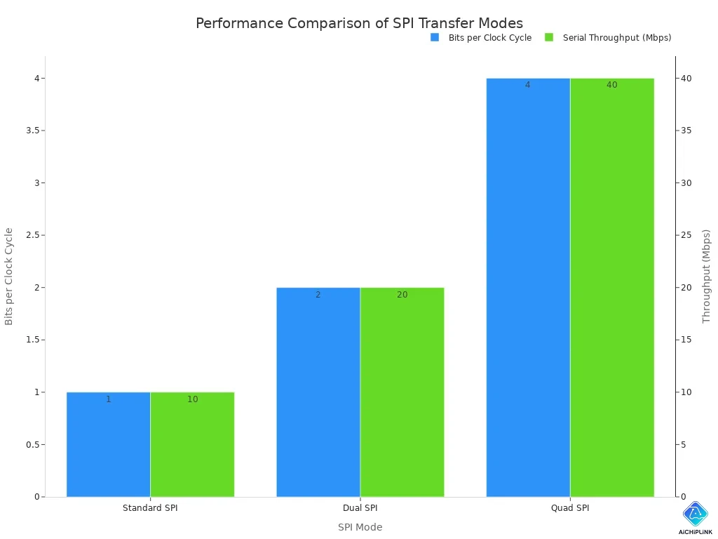
Quad SPI gives you higher speeds.
| Interface Type | Data Lines Used | Clock Cycle Bit Transfer | Typical Serial Throughput |
|---|---|---|---|
| Single SPI | 1 | 1 bit / cycle | ~10 Mbps |
| Quad SPI (QSPI) | 4 (IO0-IO3) | 4 bits / cycle | ~40 Mbps |
Quad SPI moves your data fast. It handles large files with ease.
Control Opcodes and Addressing
Your main controller sends small commands. It sends them across the spi bus. You pull Chip Select low first. Commands tell the chip to work.
Small chips use 24-bit codes. Big chips use 32-bit codes.
-
Capacity Threshold: Big SPI Flash chips need 4-byte modes.
-
Mode Switching Opcode: Enter 4-byte mode using code
0xB7. -
Mode Exit Opcode: Leave 4-byte mode using code
0xE9.
| Feature | 3-Byte Address Mode | 4-Byte Address Mode |
|---|---|---|
| Supported Capacity | Up to 128 Mb (16 MB) | 256 Mb (32 Mb) to 2 Gb (256 MB) and higher |
| Address Length | 3 Bytes (24-bit addressing) | 4 Bytes (32-bit addressing) |
| Device Support | Standard mode for legacy/smaller SPI Flash | Required for high-density SPI Flash devices |
Techs pull code from spi flash memory. They read chip code directly. This helps them test safety.
Read, Write, and Erase Cycles
Read modes do not change power. Writes and erases need extra steps. Enable Write Enable (0x06) first.
Erase steps set bits to ones. Program steps write new zeros. You check status with fast checks:
-
Polling Command: Send Read Status (
0x05) over SPI viaSPI_IOC_MESSAGE. -
Bit Checking: Check bit 0 for active operations.
-
Loop Mechanism: Run a loop until erasing ends.
-
Polling Delay: Wait 10 milliseconds using
usleep(10000).
This keeps your controller quiet. It protects your spi flash data.
SPI Flash vs Parallel Flash Memory
Pin Count and PCB Layout Efficiency
You link memory to your host processor. You use a safe spi flash interface. Old parallel flash uses many board pins. It needs over thirty pins. A small SPI Flash needs fewer pins. It uses just eight pins. You save space on your board. You use small spi parts. This spi hardware makes routing easier.
Bus Speed and Throughput Trade-Offs
Bus designs affect total speed. Parallel designs send whole bytes. They use wide board traces. Slow i2c buses send data slowly. They use just two wires. A fast spi line sends data fast. It is faster than i2c. You boost spi speed easily. Your board stays very small.
You run code from spi flash memory. This option has special trade-offs:
-
Non-Cached Execution Bottlenecks: Microcontrollers lack instruction caches. They face an spi read delay. It adds 200 ns per byte. This hurts processing speed.
-
Cache-Miss Penalties: Cache misses cause flash delays. They create lags during tasks.
-
Serial Bus Overhead: Sending code over spi limits speed. It adds extra spi delays.
Applications in Embedded Systems
Firmware and Boot Code Storage
You need memory to boot your small chips. Your system needs steady firmware for safe boots. Outside chips hold your extra firmware files. New hardware uses split spaces for safety updates.
| Parameter | Specification Value |
|---|---|
| Program / Erase Cycle Endurance | Minimum 100,000 cycles |
| Data Preservation Lifetime | Up to 20 years |
Your system bootloader uses dynamic encryption at boot. This hides your main firmware from bad spies. Safe hardware stops bad guys from stealing code. Shielding hardware lines stops hackers from taking code. Good parts keep boot firmware safe every day.
-
Partition Allocation: External chips hold update sections safely.
-
Runtime Security: Bootloaders lock data sent on normal lines.
-
Bus Integration: Normal hardware channels add easy extra storage.
Compact IoT and Automotive Hardware
Tiny smart gear and cars need fast power. Good spi bus chips add big storage capacity.
| Advantage Category | Specific Technical Benefit |
|---|---|
| PCB Design | Reduces printed circuit board footprint |
| Pin Efficiency | Operates using low pin count |
| Memory Mapping | Supports direct read access up to 256 Mbytes |
Engineers pick quick spi protocols for modern screens. Quad SPI chips store big images and font files. These graphics are too big for internal memory. Main chips read pictures using spi map modes. Display parts load graphics while main CPUs sleep.
You add a solid spi flash chip now. It keeps your car dashboard fast and quick. A small spi flash saves real board space. You get strong spi flash life in heat. Fast spi flash parts speed up all work. New spi flash designs last for years.
You pick an spi flash interface easily. A clock keeps transfers in order. This serial system needs few wires. You get steady timing. You save useful board pins.
Engineers test choices each day. You trade wide paths for fewer pins. Fast lines beat slow i2c buses. New spi chips move data fast.
| Architectural Feature | System Impact |
|---|---|
| Clock Synchronization | Uses a clock to time data transfers well. |
| Low Pin Count | Uses fewer wires for easy board layout. |
This safe memory holds your main boot code. New systems rely on this smart spi setup.

Written by Jack Elliott from AIChipLink.
AIChipLink, one of the fastest-growing global independent electronic components distributors in the world, offers millions of products from thousands of manufacturers, and many of our in-stock parts is available to ship same day.
We mainly source and distribute integrated circuit (IC) products of brands such as Broadcom, Microchip, Texas Instruments, Infineon, NXP, Analog Devices, Qualcomm, Intel, etc., which are widely used in communication & network, telecom, industrial control, new energy and automotive electronics.
Empowered by AI, Linked to the Future. Get started on AIChipLink and submit your RFQ online today!
Frequently Asked Questions
How does an spi flash chip store your data without power?
An spi flash memory uses non-volatile floating-gate transistors. These small parts hold electrical charges inside memory cells. Your board keeps system firmware safe without power. You can read saved data when power returns.
Why do microcontrollers use an spi bus instead of parallel memory?
An spi interface saves valuable board space. Parallel flash memory needs over thirty pin connections. An spi layout uses just four physical wires. Simple wiring cuts total circuit costs. It also makes trace routing easier.
What is the main difference between standard SPI and Quad SPI?
Standard spi sends one bit per clock pulse. It uses two signal wires. Quad spi uses four data lines. It moves four bits per clock tick. You get higher throughput for heavy files.
How do you erase data from your flash memory chip?
First send a write enable command byte. Next send an erase opcode. The chip changes zero blocks back to ones. Poll the status register. This checks when erasing finishes.