What Is an In-Memory Computing Chip?
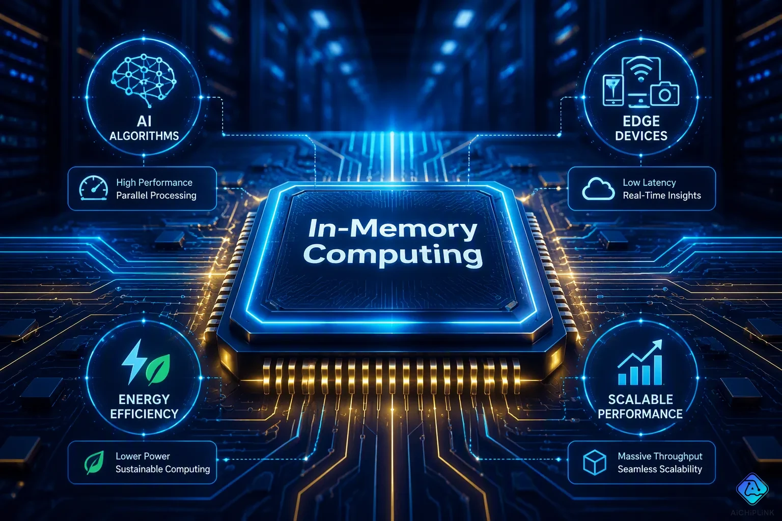
An in-memory computing chip does math right inside memory cells, so data doesn't have to travel back and forth. It's like a chef tasting and fixing a dish at the stove, instead of sending samples to a faraway lab for testing.
This design beats the "memory wall," giving faster results and much lower power use for AI tasks. Intel says it cuts power by 40-60% for memory-heavy jobs, while Micron saves 50-65%. IBM's NorthPole chip was 73 times more energy-efficient than a GPU in LLM tests.
The market shows this promise, growing from USD 3.2 billion in 2024 to a predicted USD 12.44 billion by 2033.
This article looks at the von Neumann bottleneck, explains how compute-in-memory works, and explores its future effect on AI hardware and performance.
Key Takeaways
-
In-memory computing chips do calculations inside memory cells, removing data travel and boosting speed.
-
This technology uses up to 95% less power than GPUs, so it works great for AI jobs.
-
Compute-in-memory speeds up deep learning and edge computing, making devices faster and more efficient.
-
Companies like IBM and Samsung are leading the market for these chips, which is expected to reach $12.44 billion by 2033.
-
Challenges like precision and software tools remain, but ongoing innovations promise a transformative impact on AI hardware.
The Von Neumann Bottleneck
Traditional Architecture Limits
The von Neumann architecture keeps memory and processing units separate. A CPU pulls data from memory, works on it, and sends the results back. This design ruled computing for many years. But it creates a big problem called the memory wall.
The memory wall comes from processor and memory improving at different speeds. CPU speeds followed Moore's Law, doubling every 18 months. But DRAM speed and bandwidth grew slowly, only 7-10% each year. By the 2000s, processors ran in gigahertz, while memory access still took tens of nanoseconds. This gap created a bottleneck.
| Memory Level | Latency (cycles) | Latency (nanoseconds) |
|---|---|---|
| L1 Cache | 1-4 cycles | <1 ns |
| L2 Cache | 7-14 cycles | ~3-5 ns |
| L3 Cache | 20-40 cycles | ~10-20 ns |
| RAM (Main Memory) | >100 cycles | 50-100 ns |
The table shows a huge speed gap. RAM access takes over 100 CPU cycles, but L1 cache takes only a few. This gap makes processors wait for data. Memory bandwidth also limits speed. DDR4 reaches 3.2 GT/s, while DDR5 goes from 4.8 to 8.4 GT/s. These help, but they don't fix the core design problem. This bottleneck pushed researchers to explore new designs like in-memory computing.
The High Cost of Data Movement
Moving data costs time and energy. Think of a simple task: a processor needs two numbers from RAM to add them. The CPU asks for data, waits over 100 cycles, gets the numbers, adds them, and stores the result. Most time goes to moving data, not computing.
For a typical DDR4 system with a 4-channel memory controller at 3200 MT/s, the CPU-memory bus can move 102.4 GB/s. That sounds fast, but it's still slower than processor speeds. In deep learning, data movement speed decides when inference becomes memory-bound. On old hardware, slow data movement causes delays and limits batch sizes. On new hardware, better data movement delays this problem, but it still exists.
This inefficiency pushes the need for new methods. Early ideas like near-memory computing and processing-in-memory tried to fix this by putting logic closer to data. In-memory computing chips remove this travel completely. Today, compute-in-memory chips go further, doing calculations right inside memory cells. These methods cut data movement and boost performance. Near-memory computing shortens travel distance, while processing-in-memory puts compute units inside the memory array. Compute-in-memory is the biggest change, removing data movement entirely for many tasks.
How Compute-in-Memory Works
In-memory computing is a big change in how computers work. Instead of keeping memory and processing apart, this method does math right inside the memory cells. This true compute-in-memory design removes the need to move data between separate parts. It uses proven SRAM technology, so it can be made in large numbers. It does analog math, which works well for AI inference and deep learning tasks. This approach greatly cuts down delay and energy use.
In-Memory Computing Chip Design
An SRAM-based compute-in-memory chip does dot-product operations in a set order:
-
Weight mapping – each SRAM cell stores one bit of the weight vector W. n rows stand for n weight values.
-
Input application – all input vector parts (INi) are applied at the same time to the matching bitlines. This allows parallel processing.
-
Multiplication – each stored weight Wi is multiplied by its matching input INi inside the memory cell. It uses either analog current multiplication or digital AND operations.
-
Accumulation – the products (INi·Wi) are added along the wordline. This is done by analog current/voltage sum or digital adder trees.
-
Output conversion – in analog compute-in-memory, the final sum is turned to digital using an ADC. This gives the dot-product result y.
SRAM is faster than DRAM for reading and writing, so it works well for an in-memory computing chip. The table below shows the typical access times:
| Memory Type | Typical Access Time |
|---|---|
| SRAM | 1-10 ns |
| DRAM | 30-100 ns |
SRAM gets faster access because it is on-chip memory. DRAM is off-chip memory and takes longer to access. This speed boost directly improves how fast memory operations work.
The main design parts of an SRAM-based compute-in-memory chip include:
-
SRAM cell array – stores the weight vector W. Each cell holds one bit of a weight value.
-
Multiplication circuits – built inside or attached to memory cells to do weight-input multiplication.
-
Accumulator circuits – add the multiplication results along the wordline. They use analog methods or digital adder trees.
-
Input/output interfaces – send the input vector through bitlines and give the final output.
-
Control logic – coordinates the operation order and data flow.
Key Benefits of In-Memory Computing
Compute-in-memory cuts down data movement delay in AI inference. This method mixes computation and storage into the same hardware. It removes the need to move data between separate memory and processing units. The table below shows the delay and energy benefits:
| Metric | Improvement |
|---|---|
| Energy for matrix operations | 50% reduction |
| Inference speed-up | Over 20% with very little accuracy loss |
| Computational latency (mixed-precision) | Up to 34% reduction with accuracy within 1% margin |
| Latency on mobile platforms | 21.4% reduction |
| Energy consumption reduction | Up to 1.73x |
Power use comparisons show a big difference between normal GPUs and in-memory computing chips. The table below shows the comparison:
| Metric | Traditional GPU | In-Memory (Neuromorphic) Chip |
|---|---|---|
| Power consumption (AI workloads) | 300-700 watts | 15-50 watts |
| Power savings vs. GPU | Baseline | 90-95% reduction |
| Performance-per-watt (inference) | Baseline | 20-30x better |
The HOP scheme for analog computing in memory makes matrix multiplication better for neural networks. This scheme uses digital binary words for the input vector. It keeps the weight vector in analog format. The approach lowers the needed ADC resolution to log2(2N-1) bits for a single multiplication. This is independent of the input bit width. By removing the need for high-speed DACs in processing the input matrix, the hybrid MVM core cuts costs, saves energy, and makes the system simpler. The relaxed limits on ADC/DAC converters improve compatibility with microelectronics. Using both amplitude and time for encoding increases the Euclidean distance between signal samples. This gives better noise tolerance and higher numerical precision. This compute-in-memory technique boosts AI compute acceleration for deep learning tasks.
The IBM Research analog AI chip reaches 8-bit input-output precision for matrix multiplications. This specification sets the normal precision for deep learning inference tasks on this hardware. Several companies are making in-memory computing chips for commercial use. The table below shows the current landscape:
| Company | Commercial Status | Key Detail |
|---|---|---|
| Samsung | Commercial product available | Offers Aquabolt-XL with built-in AI computing cores |
| SK hynix | Not commercialized | Decided not to sell its Newton design |
| Micron Technology | No PIM product | Bought AI startup Fwdnxt for future work |
| NeuroBlade | Product exists, commercial status unclear | Made memory with built-in processing cores for data analytics |
| Rambus | Exploratory only | Did an exploratory design for PIM DRAM |
In-memory computing also supports many AI algorithms well. The mix of lower delay, less power use, and better performance makes this compute-in-memory technology attractive for edge computing and data centers. This compute-in-memory approach gives a base for next-generation AI hardware.
Applications and Future Outlook
Transforming AI and Edge Computing
In-memory computing chips change how devices run AI algorithms. They do neural network tasks inside memory. This removes the need to move data between separate parts. The result is faster performance and lower power use.
Generative AI models benefit from this design. Compute-in-memory handles matrix multiplications well. The IBM analog AI chip reaches 8-bit precision for deep learning inference on this AI hardware.
Edge computing also gains from this technology. Mobile devices and IoT sensors need hardware that uses little power. In-memory computing chips deliver strong performance without draining batteries. The mix of low delay and energy efficiency makes compute-in-memory attractive for edge applications.
Companies like IBM, Samsung, and NeuroBlade build compute-in-memory chips. These chips support many AI algorithms well. The market grows from USD 3.2 billion in 2024 to USD 12.44 billion by 2033.
Challenges and Path to Commercialization
Despite the promise, challenges remain. Precision is a major hurdle. Analog signals are susceptible to noise, drift, and variations. These factors limit achievable precision. Analog chips require careful calibration. Training AI models digitally and mapping to analog hardware involves approximations like weight quantization. In-memory computing chips must address these precision limits.
Scalability also limits current prototypes. The current generation reaches 320 TB of memory capacity. Adding a photonic interconnect layer could push this to 1.25 PB. A prototype can reach 500 TB to 1 PB within a year. Beyond that, the architecture requires silicon implementation and single-mode fiber optics.
Software integration presents another challenge. Cross-level co-simulation tools address the lack of EDA tool-chains for memristors. The toolset includes six components: a multi-scale atomic-level simulation framework, a Kinetic Monte Carlo simulation platform, a design and technology co-optimization tool, an end-to-end simulator, a hardware emulator, and a compiler. These tools support chip design, simulation, layout, and routing.
A CIM-oriented high-level IR bridges the gap between algorithms and hardware. The compiler generates runnable codes for compute-in-memory operations like convolution and MVM. These execute on memristor arrays. Other operations run on FPGA. The tools must support different AI algorithms for broad adoption.
The path to commercialization requires solving these challenges. Better precision, advanced packaging, and mature software tools will help. Each step brings compute-in-memory closer to mainstream adoption. This technology will shape the future of AI hardware and high-performance computing.
An in-memory computing chip performs calculations directly inside memory cells. This design removes the data movement bottleneck. Processing happens faster. Power consumption drops significantly. AI workloads gain the most from in-memory computing. Generative models and edge devices run complex tasks without high energy costs. Compute-in-memory achieves strong performance for neural network operations. The technology transitions from research to commercial use. Companies like IBM and Samsung lead this effort. Software tools and precision limits require further work. Compute-in-memory will shape the future of AI hardware.

Written by Jack Elliott from AIChipLink.
AIChipLink, one of the fastest-growing global independent electronic components distributors in the world, offers millions of products from thousands of manufacturers, and many of our in-stock parts is available to ship same day.
We mainly source and distribute integrated circuit (IC) products of brands such as Broadcom, Microchip, Texas Instruments, Infineon, NXP, Analog Devices, Qualcomm, Intel, etc., which are widely used in communication & network, telecom, industrial control, new energy and automotive electronics.
Empowered by AI, Linked to the Future. Get started on AIChipLink and submit your RFQ online today!
Frequently Asked Questions
How Does an In-Memory Computing Chip Differ from a Traditional CPU?
A traditional CPU moves data between separate memory and processing units. An in-memory computing chip performs calculations directly inside memory cells. This design eliminates data travel entirely. The result is faster processing and significantly lower energy consumption for AI workloads.
Why Does Compute-in-Memory Use Less Power?
Compute-in-memory removes the energy cost of moving data across a memory bus. Traditional systems spend most of their power on data transfer, not computation. By performing math inside memory cells, compute-in-memory cuts energy use dramatically. IBM's NorthPole chip demonstrated 73 times better energy efficiency than a GPU.
What Types of AI Workloads Benefit Most from Compute-in-Memory?
Deep learning inference tasks benefit most from compute-in-memory. Matrix multiplications and dot-product operations happen naturally inside memory arrays. Generative AI models and edge computing devices gain substantial performance improvements. The technology reduces latency while maintaining accuracy within acceptable margins for most applications.
What Challenges Prevent Compute-in-Memory from Reaching the Market?
Precision remains a major hurdle for compute-in-memory chips. Analog signals suffer from noise and drift, limiting accuracy. Scalability also poses problems for large-scale deployment. Software integration requires new tools and compilers. Companies like IBM and Samsung continue developing solutions, but commercial adoption still requires further progress.
Is Compute-in-Memory Ready for Commercial Use?
Some companies offer commercial products. Samsung sells Aquabolt-XL with built-in AI computing cores. Other companies remain in development stages. The market grows from USD 3.2 billion in 2024 to a projected USD 12.44 billion by 2033. Compute-in-memory technology shows promise, but widespread adoption depends on solving precision and software challenges.