Table of Contents
- 1.0 What is the EP2C35F484C7N? (Datasheet Explained)
- 1.1 The Altera Cyclone II Family: A 90nm Workhorse
- 1.2 Decoding the Part Number: EP2C35F484C7N
- 1.3 Obsolescence Status: A Critical MRO Component
- 2.0 EP2C35F484C7N Key Technical Specifications
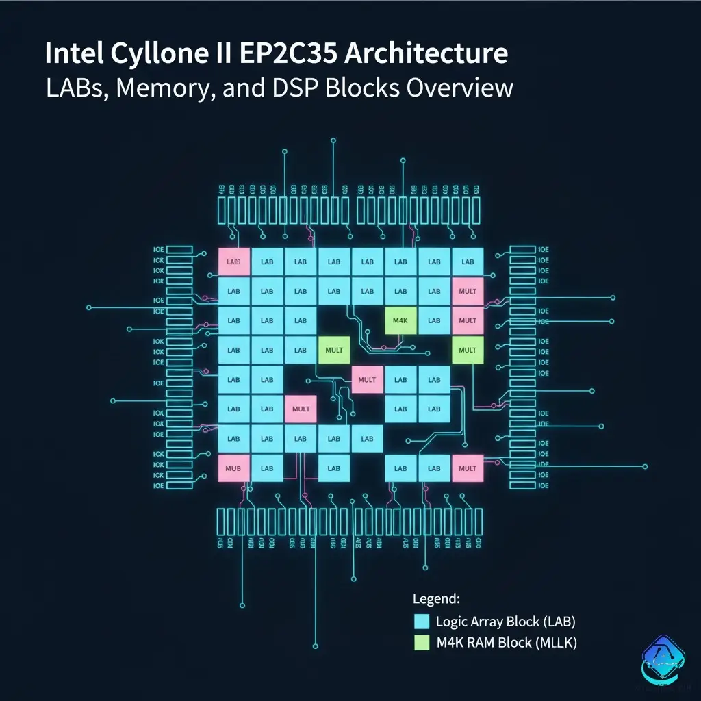
- 2.1 Core Logic, Memory, and I/O Specs
- 2.2 Understanding LEs, M4K RAM, and Multipliers
- 2.3 Operating Voltages and Package
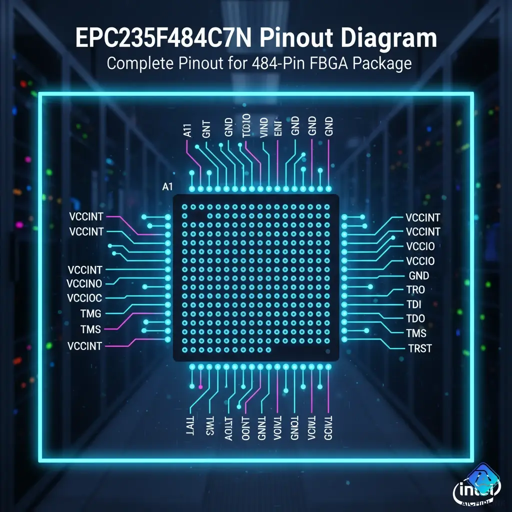
- 3.0 EP2C35F484C7N Pinout (FBGA-484 Package)
- 3.1 484-Ball FineLine BGA Pin Diagram
- 3.2 Key Pin Functions: Power, JTAG, and Configuration
- 4.0 How to Program the EP2C35F484C7N (Legacy Workflow)
- 4.1 Required Software: Legacy Altera Quartus II
- 4.2 Configuration Devices (EPCS Series)
- 4.3 Common Legacy Applications (Where to Find It)
- 4.4 Replacement and Modern Alternatives
- 5.0 Frequently Asked Questions (FAQ)
1.0 What is the EP2C35F484C7N? (Datasheet Explained)
If you're an engineer, technician, or supply chain manager working on long-life-cycle equipment, the part number EP2C35F484C7N might be all too familiar. You won't find this FPGA in a new 2025 consumer gadget. Instead, this chip is a veteran, a workhorse from the Altera Cyclone II family that was the backbone of industrial, automotive, and communications hardware in the mid-2000s.
Why are we talking about a 20-year-old chip? Because the global market for MRO (Maintenance, Repair, and Operations) for this legacy equipment is massive. A 2023 report on industrial automation highlighted that the average lifespan of factory equipment now frequently exceeds 15-20 years. When a control board on a $250,000 piece of medical imaging equipment or a factory PLC line fails, you don't "just upgrade it." You repair it.
And that repair often hinges on sourcing this one specific, obsolete component. This guide is your technical deep-dive into the EP2C35F484C7N datasheet. We'll cover its specs, pinout, and the critical (and tricky) legacy software you need to work with it.
1.1 The Altera Cyclone II Family: A 90nm Workhorse
The Cyclone II family, originally from Altera (now Intel), was a game-changer. It was one of the first FPGA families built on a 90-nm process, which allowed for a massive increase in logic density and features at a cost low enough to compete with ASICs for high-volume applications.
Its core value proposition was:
- Low Cost: It was purpose-built to be the low-cost FPGA solution.
- High Density: Offered a significant number of logic elements for its price.
- SRAM-Based: Like all modern FPGAs, it's SRAM-based, meaning its configuration is volatile and must be loaded from an external flash chip at power-on.
- Rich Feature Set: It was one of the first low-cost families to include dedicated embedded multipliers for DSP tasks and M4K RAM blocks, which were 4-kbit blocks of on-chip memory.
- PLLs: Integrated Phase-Locked Loops for flexible clock management.
1.2 Decoding the Part Number: EP2C35F484C7N
The part number tells you the complete story of the chip:
- EP2C: Identifies the device as an Altera Cyclone II.
- 35: The device density. This is one of the larger chips in the family, with 33,216 Logic Elements (LEs).
- F484: The package type: a 484-pin FineLine BGA (FBGA).
- C7: This denotes the Temperature Grade and Speed Grade.
- C: Commercial (0°C to 85°C).
- -7: A standard speed grade (faster is -6, slower is -8).
- N: Indicates the device is lead-free (RoHS compliant).
1.3 Obsolescence Status: A Critical MRO Component
Official Status: OBSOLETE / END-OF-LIFE (EOL)
Let's be perfectly clear: the EP2C35F484C7N and the entire Cyclone II family are obsolete. They are no longer manufactured by Intel and are Not Recommended for New Designs (NRND).
This part's entire value today is as a critical MRO (Maintenance, Repair, and Operations) component. Because it is in a specific 484-ball BGA package and requires a specific legacy software version, there is no drop-in replacement. Repairing a board with a failed EP2C35F484C7N requires sourcing a genuine, identical part.
2.0 EP2C35F484C7N Key Technical Specifications
When you're sourcing a replacement, matching the EP2C35F484C7N specs is non-negotiable.
2.1 Core Logic, Memory, and I/O Specs
This table summarizes the core resources available on this device.
| Feature | Specification |
|---|---|
| Family | Cyclone II |
| Logic Elements (LEs) | 33,216 |
| Logic Array Blocks (LABs) | 2,076 |
| Total RAM Bits | 483,840 bits |
| M4K RAM Blocks | 105 (4,096 bits each) |
| Embedded Multipliers | 35 (18-bit x 18-bit) |
| PLLs (Phase-Locked Loops) | 4 |
| Maximum User I/O | 322 |
2.2 Understanding LEs, M4K RAM, and Multipliers
- Logic Element (LE): This is the fundamental building block. In the Cyclone II, each LE contains a 4-input look-up table (LUT) for combinational logic, a programmable flip-flop for registered logic, and fast-carry chain logic.
- M4K RAM Blocks: These are 4-kbit blocks of dedicated on-chip memory. The 483,840 total RAM bits are what made this chip so powerful for its time, allowing for deep data buffers (FIFOs) and processor instruction/data memory.
- Embedded Multipliers: The 35 dedicated 18x18 multipliers mean you can perform high-speed math for DSP or video processing without using up thousands of LEs.
2.3 Operating Voltages and Package
This is a critical specification for any MRO work.
- Core Voltage (VCCINT): 1.2V (±5%)
- I/O Voltage (VCCIO): 1.5V, 1.8V, 2.5V, or 3.3V (The I/O banks are independent and can interface with 3.3V logic).
- Package: 484-pin FineLine BGA (FBGA) with a 1.0 mm ball pitch.
- Temperature Range: Commercial (0°C to 85°C).
3.0 EP2C35F484C7N Pinout (FBGA-484 Package)
The EP2C35F484C7N pinout corresponds to the 484-ball BGA. This is a high-pin-count, surface-mount package. Any attempt to replace this chip requires a professional BGA rework station and, ideally, X-ray inspection to check for solder joint integrity.
3.1 484-Ball FineLine BGA Pin Diagram
3.2 Key Pin Functions: Power, JTAG, and Configuration
When a board fails, you don't probe all 322 I/O pins. You check these critical support pins first.
| Pin Type | Name(s) | Function |
|---|---|---|
| Core Power | VCCINT | 1.2V core logic supply. There are many of these pins; all must be stable. |
| I/O Power | VCCIO (Banks 1-8) | 1.5V to 3.3V. Each I/O bank can be powered independently. |
| PLL Power | VCCA, VCCD | Dedicated 1.2V Analog and Digital power for the PLLs. Must be clean. |
| Ground | GND | Numerous ground pins. All must have a solid connection. |
| JTAG | TCK, TDI, TDO, TMS | The JTAG test/programming port. This is how you test and configure the chip. |
| Configuration | MSEL0, MSEL1, nCE | Mode-select pins. Hard-wired on the PCB to set the boot mode (e.g., Active Serial). |
| Config Data | DCLK, DATA0, nCS, ASDI | The pins used to load the configuration from an external serial flash (EPCS) chip. |
| Status | nSTATUS, CONF_DONE | These pins report the status of the configuration. If CONF_DONE is low, the FPGA is not booted. |
4.0 How to Program the EP2C35F484C7N (Legacy Workflow)
This is the single biggest challenge for engineers new to this device. You cannot use modern Intel Quartus Prime software.
4.1 Required Software: Legacy Altera Quartus II
To program, compile, or even just test an EP2C35F484C7N, you must use a specific legacy version of the Altera design software.
- Software Name: Altera Quartus II (not Intel Quartus Prime).
- Compatible Version: Version 13.0sp1 is the last version of Quartus II to provide support for the Cyclone II family.
- OS Compatibility: This 32-bit legacy software runs best on older operating systems like Windows 7 or Windows XP. Running it inside a virtual machine (VM) is a very common and recommended practice for modern PCs.
- Programming Hardware: You need a compatible JTAG programming cable, such as the classic Altera USB-Blaster.
4.2 Configuration Devices (EPCS Series)
The EP2C35F484C7N is SRAM-based, so its configuration is volatile (lost on power-down). It needs to boot from an external non-volatile chip.
- Configuration Scheme: Typically uses Active Serial (AS) mode.
- Required Configuration Chip: It is designed to boot from an EPCS serial configuration device, such as the EPCS16 (16-Mbit) or EPCS64 (64-Mbit) flash memory chips.
- Boot Process: At power-on, the FPGA acts as the bus master, provides a clock (DCLK), and pulls the configuration data (
.poffile) from the EPCS chip into its internal SRAM. If this EPCS chip is corrupted or fails, the FPGA will not boot.
4.3 Common Legacy Applications (Where to Find It)
This FPGA was a high-density "brains" for a wide range of products. You will find it in:
- Industrial Automation: PLCs, complex motor control drivers, and HMI (Human-Machine Interface) panels.
- Video Processing: Simple video scalers, format converters, and broadcast test equipment.
- Telecommunications: Network line cards, data processing units, and protocol bridges.
- Medical Equipment: Ultrasound machines, patient monitoring systems, and lab analysis equipment.
- Test & Measurement: The logic core for oscilloscopes, logic analyzers, and function generators from the mid-2000s.
4.4 Replacement and Modern Alternatives
When your EP2C35F484C7N fails, you have two choices, one of which is much harder than the other.
| Option | Strategy | Required Effort |
|---|---|---|
| Direct Repair (MRO) | Source a genuine, identical EP2C35F484C7N. | Low (Sourcing), High (BGA Rework). |
| Modern Redesign | Redesign the PCB with a modern Cyclone 10 LP or AMD/Xilinx Artix-7 FPGA. | Extremely High. Requires new PCB, new power (1.0V), new software (Quartus Prime/Vivado), and porting the design. |
Conclusion: A Critical MRO Workhorse
The EP2C35F484C7N FPGA is a true classic. It represents a generation of FPGAs that brought high-density logic, on-chip RAM, and DSP functions to the mass market. Today, its role has shifted from innovation to sustainment. For the thousands of critical systems worldwide that rely on this chip, it is an indispensable component.
Working with this device requires specialized legacy knowledge, the correct (and old) software tools, and a trusted supply chain partner. Sourcing a high-pin-count BGA part that is long obsolete is a high-risk operation. You cannot afford to risk a line-down situation on a counterfeit or improperly handled component.
If you are facing the challenge of sourcing this or other obsolete FPGAs, you need a partner who understands this market. Explore our full catalog of FPGAs or contact AichipLink today for a quote on the genuine, reliable legacy components you need.

Written by Jack Elliott from AIChipLink.
AIChipLink, one of the fastest-growing global independent electronic components distributors in the world, offers millions of products from thousands of manufacturers, and many of our in-stock parts is available to ship same day.
We mainly source and distribute integrated circuit (IC) products of brands such as Broadcom, Microchip, Texas Instruments, Infineon, NXP, Analog Devices, Qualcomm, Intel, etc., which are widely used in communication & network, telecom, industrial control, new energy and automotive electronics.
Empowered by AI, Linked to the Future. Get started on AIChipLink.com and submit your RFQ online today!
Frequently Asked Questions
What is the EP2C35F484C7N?
The EP2C35F484C7N is a legacy FPGA from the **Altera (now Intel) Cyclone II** family. It features **33,216 Logic Elements (LEs)**, 483,840 bits of RAM, 35 embedded multipliers, and 322 user I/O pins. It is in a **484-pin FineLine BGA (FBGA)** package, has a 1.2V core, and a C7 (Commercial, -7 speed) grade.
Is the EP2C35F484C7N obsolete?
Yes, the **EP2C35F484C7N** and the entire Cyclone II family are **obsolete (End-of-Life)**. They are no longer manufactured by Intel. They are **Not Recommended for New Designs (NRND)** and are sourced today only for the maintenance and repair (MRO) of existing equipment.
What software do I use to program the EP2C35F484C7N?
You must use a legacy version of the **Altera Quartus II** development software, such as **v13.0sp1**, which was the last version to support the Cyclone II family. Modern Intel Quartus Prime software does **not** support this device. You will also need a programming cable like the Altera USB-Blaster.
What is the difference between EP2C35F484C7N and EP2C5F256C6N?
Both are Cyclone II FPGAs, but the **EP2C35** is a much larger and more capable device. * **EP2C35F484C7N:** **33,216 LEs**, 483 kbits RAM, 35 Multipliers, 4 PLLs, 322 I/O. * **EP2C5F256C6N:** **4,608 LEs**, 119 kbits RAM, 13 Multipliers, 2 PLLs, 172 I/O. They are not interchangeable.
What is the configuration device for an EP2C35F484C7N?
The EP2C35F484C7N is SRAM-based (volatile) and requires an external configuration device. It is typically paired with an **Altera EPCS** serial configuration flash chip, such as an **EPCS16** or **EPCS64**.