The name looks intimidating — twelve characters, three number groups, one letter suffix — but every field is a specification in disguise. Once decoded, XA7A25T-1CPG238Q tells you the manufacturer family, the device density, the speed grade, the package footprint, and the qualification level, all in a single string. More importantly, the "XA" prefix at the front changes the entire design context: this is not a commercial FPGA placed in a warm enclosure. It is a semiconductor device qualified to AEC-Q100 Grade 2, designed to run in the instrument cluster of a moving car at −40°C on a cold winter morning and still be functional after a decade of thermal cycling.
Before diving into what the XA7A25T-1CPG238Q can do, it is worth asking the question that separates useful from superficial FPGA coverage: why does an automotive application need an FPGA at all, when most automotive functions are handled by microcontrollers and dedicated ASICs? The answer is in the word "programmable" — when a camera-based ADAS system needs real-time lane detection, when a digital instrument cluster needs to render vector graphics from multiple CAN sources simultaneously, when a LiDAR pre-processor needs custom signal conditioning before the data reaches a main SoC — none of these have a commodity IC that handles them exactly right. The FPGA fills the gap, and the XA qualification ensures it fills that gap reliably across the vehicle's service life.
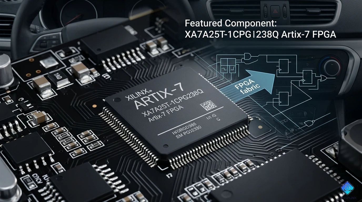
1.0 Full Part Number Decoded: XA7A25T-1CPG238Q Character by Character
AMD Xilinx FPGA part numbers are structured identifiers. Here is the complete decode for XA7A25T-1CPG238Q:
XA — Product family / qualification grade:
- X = Xilinx (now AMD Xilinx)
- A = Automotive grade (AEC-Q100 qualified). The full XA prefix distinguishes the automotive-qualified silicon from the commercial-grade XC prefix (XC7A25T would be the commercial equivalent) and the military/space-grade XQ prefix
7 — Device generation: 7-Series (the generation that includes Artix-7, Kintex-7, Virtex-7, and Zynq-7000)
A — Sub-family within 7-Series: A = Artix-7 (lowest-cost, lowest-power member of the 7-series family; higher tiers are K = Kintex-7, V = Virtex-7, Z = Zynq-7000)
25T — Device density code:
- 25 = density identifier (maps to approximately 23,360 logic cells, 80 DSP slices, 45 36Kb block RAMs)
- T = package type indication / logic cell tier (T = standard density configuration within this family)
-1 — Speed grade:
- -1 = slowest/most conservative speed grade for this family
- -2 = mid speed grade (faster timing, same silicon, different screening)
- -3 = fastest speed grade (for XC commercial devices; automotive XA parts use -1 and -2) The speed grade determines the guaranteed timing specifications — propagation delays, setup/hold times, maximum clock frequencies achievable.
C — Temperature / operating grade:
- C = Commercial (0°C to +85°C) — but this "C" in the package code has a different meaning when combined with XA prefix. The automotive qualification overrides — see Section 3 for the actual operating range
PG — Package body type:
- P = Plastic (vs. ceramic for military)
- G = BGA (Ball Grid Array) family identifier
238 — Ball count: 238 solder balls in the CPG238 CSPBGA (Chip Scale Ball Grid Array) package
Q — Qualification suffix:
- Q = AEC-Q100 automotive qualification (the definitive qualifier that makes this an automotive-grade part)
2.0 Specifications — What This Device Actually Contains
Key parameters from the AMD Xilinx XA7A25T product documentation:
Logic Fabric:
- Logic cells: 23,360 (note: some distributor listings incorrectly state "25K" — the datasheet value is 23,360)
- Slices: 3,650 (each slice contains 4 LUT6 + 8 flip-flops)
- LUT6s: 14,600 six-input look-up tables, configurable as logic or distributed memory
- Flip-flops: 29,200
Memory:
- Block RAM: 45 × 36 Kb blocks = 1,620 Kb (1.58 Mb) total on-chip block RAM
- Configurable as true dual-port or simple dual-port in 18 Kb or 36 Kb modes
- Distributed RAM: Derived from LUT fabric; approximately 185 Kb additional
DSP:
- DSP48E1 slices: 80
- Each DSP48E1 contains a pre-adder, 18×25 multiplier, and 48-bit accumulator
- Peak DSP performance: 264 GMAC/s (at maximum clock rate)
I/O and Serial:
- User I/O (in CPG238 package): 106 pins
- High-speed serial transceivers: 4× GTP transceivers, 500 Mb/s to 6.6 Gb/s each
- Supported protocols: PCIe Gen1/Gen2 (1-lane), GigE, SATA, USB 3.0 PHY, DisplayPort, custom SerDes
- Maximum I/O bandwidth: up to 52 Gb/s aggregate (includes transceiver bandwidth)
Clock Management:
- CMT (Clock Management Tile): 2× CMTs, each containing 1× MMCM (Mixed-Mode Clock Manager) + 1× PLL
- Total: 2× PLLs + 2× MMCMs
- Supports clock multiplication, division, phase shifting, and deskew
Analog Integration (XADC):
- Dual 12-bit ADC: 1 MSPS each, 17 multiplexed analog input channels
- Temperature sensor and supply voltage monitoring built in
- Configurable in simultaneous-sampling or multiplexed-sampling modes
Configuration and Security:
- Configuration interfaces: JTAG, SPI (x1/x2/x4), SelectMAP (x8/x16/x32), Serial
- AES-256 encryption of configuration bitstream
- HMAC/SHA-256 authentication
- Built-in SEU (Single Event Upset) detection and correction for block RAM
Process and Power:
- Process: 28nm HPL (High Performance Low power) HKMG (High-K Metal Gate)
- Core voltage (VCCINT): 1.0V nominal
- I/O voltage (VCCO): Configurable per bank — 1.2V, 1.5V, 1.8V, 2.5V, 3.3V
- Auxiliary supply (VCCAUX): 1.8V
Package:
- CPG238: CSPBGA (Chip Scale Plastic Ball Grid Array), 238 balls
- Body dimensions: 9.0 mm × 9.0 mm
- Ball pitch: 0.5 mm
- Board area: compact, suitable for space-constrained automotive ECU designs
Qualification:
- AEC-Q100 Grade 2 (−40°C to +105°C junction temperature; automotive grade)
- Operating range: −40°C to +125°C junction temperature (as stated on TI and distributor pages — verify against current AMD datasheet for exact rating)
- ISO/TS 16949 manufacturing quality
3.0 What "XA" Really Means: Beyond Temperature Grade
The most important thing to understand about the XA prefix is that it does not simply mean "this chip works at lower temperatures." The XA qualification represents a fundamentally different supply chain, screening, and lifecycle commitment that affects how you design with and around the part.
AEC-Q100 Grade 2 qualification means the device has passed a battery of accelerated stress tests defined by the Automotive Electronics Council: high-temperature storage (1,000 hours at 150°C), temperature cycling (1,000 cycles, −40°C to +125°C), humidity-biased life test, electrical characterization at temperature extremes, and multiple others. Commercial-grade XC7A25T parts are not required to pass these tests. A commercial part that appears to work at automotive temperatures in bench testing has not been qualified to the same standard — it may fail at field conditions after months or years of thermal cycling.
Long lifecycle commitment: AMD Xilinx commits to production continuity for XA automotive parts far beyond the lifecycle commitment for commercial parts. Automotive designs have 5–10+ year development cycles and 15–20+ year production and field service windows. A commercial FPGA can be discontinued when market demand shifts; an XA automotive part is under a much longer commitment aligned with automotive Tier-1 supplier requirements.
PPAP documentation support: For automotive Tier-1 suppliers, component changes in a production design require a Production Part Approval Process (PPAP) submission to the OEM. XA parts are supported with the documentation (SPC data, failure mode analysis, engineering change notification procedures) that PPAP requires. Commercial components typically lack this documentation infrastructure.
Change notification: AMD Xilinx commits to providing advance notice of any significant product changes (process revisions, package changes) to XA automotive customers — allowing time for requalification before production impact. This is a formal commitment absent from commercial product supply terms.
The practical design impact: You cannot simply substitute an XC7A25T for an XA7A25T in an automotive application and declare compliance. The silicon may be electrically identical at the time of design, but the supply chain, documentation, qualification, and lifecycle commitments are different categories of product.
4.0 Automotive and Industrial Applications
The XA7A25T-1CPG238Q's combination of features — automotive qualification, 23,360 LCs, 4 high-speed serial transceivers, integrated XADC, hardware security, and compact CPG238 package — makes it well suited for specific application categories:
Advanced Driver Assistance Systems (ADAS): The GTP transceivers enable high-bandwidth sensor interfaces. A camera-based ADAS subsystem might use GTP lanes for MIPI CSI-2 to SerDes deserializer output, carrying raw camera data at several Gb/s. The FPGA's programmable logic then performs pre-processing — image reformatting, frame synchronization, bayer pattern demosaicking — before forwarding processed video to the ADAS SoC. The XADC provides in-system monitoring of supply voltages, useful for detecting electrical anomalies that could compromise ADAS function.
In-Vehicle Infotainment (IVI) and Digital Instrument Clusters: The 4 GTP transceivers support DisplayPort or FPD-Link III output directly, enabling the FPGA to drive high-resolution displays from multiple data sources while managing source switching, format conversion, and timing generation. The 80 DSP slices support real-time graphics operations including pixel blending and format conversion.
Motor Control and Power Electronics: For EV or hybrid vehicle motor controllers, the FPGA's parallel logic architecture handles the deterministic high-frequency PWM generation, current feedback measurement (using the XADC), and encoder decoding at rates impossible for software-based MCU implementations. The −40°C low-end qualification is critical in engine bay environments that see extreme cold-start conditions.
Vehicle LiDAR / Radar Signal Processing: Time-of-flight LiDAR systems generate extremely high sample-rate data (hundreds of MSPS) that must be processed before reaching the main compute SoC. The XA7A25T's logic fabric implements range calculation, point cloud formation, and noise filtering. The GTP transceivers deliver the pre-processed data over a high-speed serial link.
Industrial automation (leveraging the same die): Outside automotive, the same device serves industrial motor drives, machine vision preprocessing, test equipment front-ends, and communications protocol bridging — applications where the AEC-Q100 qualification provides margin over commercial grade in harsh industrial environments.
5.0 Five Misconceptions About This Part
Misconception 1: "The 7A25T has 25,000 logic cells"
The "25" in the device name is a density identifier, not an exact cell count. The actual logic cell count in the XA7A25T is 23,360. This matters when estimating utilization for a given design — planning for 25K cells and finding 23.4K available is a 6.5% shortfall that can affect fitment decisions. Always use the exact figure from the AMD product page or DS180 data sheet, not the approximate name-derived number.
Misconception 2: "Any Artix-7 FPGA can be used in automotive designs after temperature testing"
Temperature testing alone does not make a commercial FPGA automotive-qualified. AEC-Q100 qualification involves stress tests beyond temperature — electromigration, hot carrier injection, time-dependent dielectric breakdown — that probe the silicon's reliability characteristics over time, not just its performance at temperature. A commercial XC7A25T that passes your bench testing at −40°C and +125°C has not undergone these stress qualifications. Placing it in an automotive application without XA qualification creates liability and potentially safety risk.
Misconception 3: "The -1 speed grade is the slowest and therefore worst choice"
Speed grade selection is about fitting your timing requirements, not about choosing the fastest available. A -1 speed grade device has slower timing specs than -2, but if your design closes timing at -1, it is the better choice for an automotive application because: (1) it comes from a more conservative selection of the same silicon — devices that do not meet faster speed grades are often screened into slower grades, making -1 parts the most abundant; (2) for AEC-Q100 compliance, the timing specifications must be met over the full −40°C to +125°C range, and -1 specifications are guaranteed over this range; (3) the price premium for -2 speed grade is not justified if -1 timing closure is achievable.
Misconception 4: "The XADC can replace external ADCs for precision signal acquisition"
The XADC's 12-bit, 1 MSPS ADC is appropriate for monitoring and housekeeping measurements — supply voltages, die temperature, and slowly-varying signals from sensors. For precision signal acquisition where the FPGA's bitstream is making decisions based on analog measurements, the XADC's 12-bit resolution and the noise floor contributed by on-chip digital switching are significant limitations. The XADC is not a replacement for a precision 16-bit or 24-bit sigma-delta ADC when high-accuracy analog measurement is required. Use the XADC for power management and system health monitoring; use an external ADC for precision signal acquisition.
Misconception 5: "Vivado licensing works the same for XA automotive parts as for commercial XC parts"
AMD Xilinx's Vivado Design Suite supports both XA and XC 7-series devices in the same tool. The XA7A25T appears in the Vivado device list and can be targeted directly. However, IP cores that are licensed per device family may require verification that the automotive device is within the licensed scope. Additionally, for designs targeting AEC-Q100 qualified production, the design flow documentation (implementation reports, timing analysis) may need to be retained as part of the automotive qualification documentation package — a requirement that does not apply to commercial designs.
6.0 Design Essentials: Power, Clocks, Configuration, and PCB
Power supply requirements:
The XA7A25T requires three main power domains:
- VCCINT = 1.0V ± 3%: Core logic supply. Current depends heavily on utilization and clock frequency — estimate 50–200 mA for typical designs; use TI's XPower or AMD's Power Estimator tool for accurate figures
- VCCAUX = 1.8V ± 5%: Auxiliary supply for configuration logic, XADC, PLLs, and I/O buffers
- VCCO (per I/O bank): Each I/O bank has an independent VCCO supply, configurable to 1.2V, 1.5V, 1.8V, 2.5V, or 3.3V depending on the interface standard. The GTP transceiver banks have their own MGTAVCC (1.0V) and MGTAVTT (1.2V) supplies
For automotive reliability, decouple each power supply with bulk capacitance (10–47 µF) plus high-frequency bypass capacitors (100 nF per power pin) placed within 3 mm of each power ball cluster.
Clock management:
The CPG238 package has dedicated clock input pins (GCLK, regional clock, and multi-region clock resources). For automotive designs, the MMCM's frequency synthesis capability (from an input reference clock) allows generation of all required on-chip clock domains from a single board-level crystal oscillator, reducing BOM complexity. The MMCM's spread-spectrum clocking output can reduce EMI emissions — a parameter that automotive designs must meet for CISPR 25 compliance.
Configuration and bitstream security:
In automotive designs, the configuration bitstream should always be AES-256 encrypted. An unencrypted bitstream stored in an SPI flash can be read and reverse-engineered by anyone with physical access to the board — a significant IP and safety concern for ADAS and powertrain control logic. Enable encryption during bitstream generation in Vivado (Encrypt option in Bitstream Settings), and store the key in the FPGA's battery-backed or one-time-programmable eFUSE registers. The HMAC/SHA-256 authentication prevents bitstream tampering.
PCB layout for GTP transceivers:
The 4× GTP transceivers in the XA7A25T require AC-coupled differential routing on the PCB. Key rules: 100 Ω differential impedance (±5%), maximum 10 inches trace length for rates above 3 Gb/s, matched length within pair (±5 mil), no vias in the differential trace pair if possible (backdrilled vias if mandatory), AC coupling capacitors (100 nF, 0402 or smaller) within 1 cm of the FPGA balls for the TX output.
7.0 Real Questions from FPGA Engineers
Q: Can I prototype my design using a commercial XC7A25T evaluation board and then move to the XA7A25T for production? Are they pin-compatible?
A: Yes, this is the intended AMD Xilinx flow. The XA7A25T and XC7A25T are pin-compatible in the same CPG238 package — the same Vivado project targeting XA7A25T can be loaded on hardware built around XC7A25T during prototyping, and the same PCB footprint is used for both. The silicon is the same die; the differences are in testing, qualification, and supply chain. This is specifically why AMD Xilinx provides commercial-grade Artix-7 devices for prototyping before automotive qualification sign-off: it allows the design to be fully developed and verified using available development boards (Arty A7, Basys 3, etc.) before transitioning to the production XA device.
Q: The XA7A25T-1CPG238Q has only 106 user I/O pins in the CPG238 package. My design needs more. Can I use a larger package?
A: The Artix-7 25T device is only available in the CPG238 package — this is a die-level density constraint, not a packaging choice. If you need more I/O, you must move to a higher-density XA Artix-7 device in the same family: XA7A35T (CPG236 or FGG484), XA7A50T (FGG484 or CSG325), XA7A75T (FGG484), or XA7A100T (FGG484 or CSG324). All XA Artix-7 devices share the same Vivado tool support and similar architecture, so moving up in density preserves your IP investment. Note that larger devices may require different power supply current ratings and PCB footprint adjustments.
Q: I need AEC-Q100 Grade 1 (−40°C to +125°C junction temperature) compliance for my application. Does XA7A25T meet Grade 1?
A: AEC-Q100 Grade 2 covers −40°C to +105°C junction temperature. Grade 1 covers −40°C to +125°C. Some sources list the XA7A25T as supporting up to +125°C operation — verify the exact grade against the current AMD Xilinx XA Artix-7 product documentation and the specific AEC-Q100 qualification report for your intended application. For safety-critical automotive functions that must demonstrate AEC-Q100 Grade 1 qualification, request the qualification test summary from AMD Xilinx or an authorized distributor to confirm the exact grade level the XA7A25T-1CPG238Q is certified to, as grade distinctions affect functional safety documentation and OEM component approval processes.
Q: Does the XA7A25T-1CPG238Q support ISO 26262 functional safety requirements for ADAS designs?
A: The XA7A25T-1CPG238Q's hardware features — AES bitstream encryption, HMAC authentication, built-in SEU detection for block RAM — contribute to a safety architecture, but the device itself is not ISO 26262 certified as an ASIL-rated component in the same way that dedicated safety MCUs are. For an ISO 26262 compliant ADAS design using this FPGA, the system integrator is responsible for implementing the safety concept at the system level: using the FPGA as a logic element within a safety architecture that includes independent monitoring, redundancy, or diversity as appropriate for the target ASIL level. AMD Xilinx provides functional safety design documentation (Failure Modes and Effects Analysis, SEU injection test reports) to support customer safety cases. Consult AMD Xilinx's functional safety resources and engage with their field application engineering team for your specific ASIL target.
8.0 Quick Reference Card
Part Number Decode:
| Characters | Meaning |
|---|---|
| XA | Automotive grade (AEC-Q100, long lifecycle) |
| 7 | 7-Series generation |
| A | Artix-7 sub-family (lowest cost/power) |
| 25T | Device density (≈23,360 LCs, 80 DSPs) |
| -1 | Speed grade (conservative, -2 is faster) |
| C | Plastic package, commercial temperature code |
| PG | Ball Grid Array (BGA) package type |
| 238 | 238 solder balls |
| Q | AEC-Q100 qualification confirmed |
Key Resources at a Glance:
| Resource | Count |
|---|---|
| Logic cells | 23,360 (not 25K) |
| Slices (4 LUT6 + 8 FF each) | 3,650 |
| DSP48E1 slices | 80 |
| Block RAM (36 Kb each) | 45 |
| Total block RAM | 1,620 Kb |
| GTP transceivers | 4× (up to 6.6 Gb/s each) |
| User I/O (CPG238) | 106 pins |
| CMTs (PLL + MMCM) | 2 |
| XADC | Dual 12-bit, 1 MSPS |
| Package body | 9 × 9 mm, 0.5 mm pitch |
Power Domains:
| Supply | Voltage | Function |
|---|---|---|
| VCCINT | 1.0V ± 3% | Core logic |
| VCCAUX | 1.8V ± 5% | PLLs, config, XADC |
| VCCO | Bank-configurable | I/O (1.2–3.3V per bank) |
| MGTAVCC | 1.0V | GTP transceiver core |
| MGTAVTT | 1.2V | GTP transceiver termination |
XA (Automotive) vs XC (Commercial) — Key Differences:
| XA7A25T | XC7A25T | |
|---|---|---|
| AEC-Q100 | ✅ Grade 2 | ❌ Not qualified |
| Operating temp | −40°C to +105°C (Tj) | 0°C to +85°C (Tj) |
| Lifecycle commitment | Automotive long-term | Commercial standard |
| PPAP documentation | ✅ Supported | ❌ Not available |
| Change notification | Formal automotive PCN | Standard |
| Prototyping use | Yes (same Vivado flow) | Yes (same die) |
| Pin-compatible (CPG238) | ✅ Yes | ✅ Yes |
For sourcing AMD Xilinx XA7A25T-1CPG238Q with verified authenticity and automotive-grade documentation, visit aichiplink.com.

Written by Jack Elliott from AIChipLink.
AIChipLink, one of the fastest-growing global independent electronic components distributors in the world, offers millions of products from thousands of manufacturers, and many of our in-stock parts is available to ship same day.
We mainly source and distribute integrated circuit (IC) products of brands such as Broadcom, Microchip, Texas Instruments, Infineon, NXP, Analog Devices, Qualcomm, Intel, etc., which are widely used in communication & network, telecom, industrial control, new energy and automotive electronics.
Empowered by AI, Linked to the Future. Get started on AIChipLink and submit your RFQ online today!
Frequently Asked Questions
What is XA7A25T-1CPG238Q used for?
The XA7A25T-1CPG238Q is an automotive-grade Artix-7 FPGA designed for applications requiring high reliability and flexibility, such as ADAS systems, digital instrument clusters, LiDAR preprocessing, and industrial control; its programmable logic enables real-time data processing and interface bridging where fixed-function ICs are insufficient.
What does the “XA” prefix mean in this FPGA?
The “XA” prefix indicates automotive qualification under AEC-Q100 standards, meaning the device is tested for extreme conditions like thermal cycling, high-temperature operation, and long lifecycle reliability, making it fundamentally different from commercial-grade XC devices in terms of durability, documentation, and supply stability.
How powerful is the XA7A25T FPGA?
This FPGA integrates 23,360 logic cells, 80 DSP slices, 45 block RAMs, and 4 high-speed GTP transceivers up to 6.6 Gb/s, providing sufficient performance for mid-range signal processing, embedded vision preprocessing, and high-speed communication tasks in automotive and industrial systems.
Can XA7A25T replace a microcontroller or ASIC?
Not directly—while it can outperform microcontrollers in parallel processing and real-time control, the XA7A25T is typically used alongside MCUs or SoCs to handle custom logic acceleration, high-speed interfaces, or deterministic processing tasks that fixed ASICs or software-based systems cannot efficiently achieve.
Is XA7A25T pin-compatible with XC7A25T for prototyping?
Yes, XA7A25T is pin-compatible with the commercial XC7A25T in the same package, allowing developers to prototype using widely available evaluation boards and later migrate to the automotive-grade version for production without redesigning the PCB.