What Is M425R1GB4BB0? The "GB4" Does Not Mean 4 Gigabytes — and the "1Rx16" Tells You More About Performance Than Any Speed Spec
Two things in the M425R1GB4BB0 part number are commonly misread, and both affect how this module should be specified and evaluated.
The first: GB4 does not mean 4 gigabytes. In Samsung's module naming convention, "GB" here encodes the die density and die width — specifically 8 Gb (8 gigabit) per die, with x16 organization per die (4 chips across the 64-bit DDR5 data bus). The "4" in GB4 refers to the number of die packages on the module, not to gigabytes of capacity. The module's actual capacity is 8 gigabytes — derived from 4 chips × 8 Gb = 32 Gb / 8 bits = 4 GB per half, × 2... or more precisely from the complete 1024M × 64-bit organization. The marketing label and the actual capacity match, but the path from the part number to that capacity requires understanding what GB4 actually encodes.
The second: 1Rx16 matters more for performance than the DDR5-4800 speed rating. In a 1Rx16 SO-DIMM, each chip is x16 wide, and there is only one rank. The entire 64-bit DDR5 bus is served by 4 chips in a single rank. By contrast, a 2Rx8 SO-DIMM uses 16 chips arranged in two ranks of 8 chips each — each chip contributing 8 bits to the 64-bit bus. The 2Rx8 configuration allows rank interleaving, where the memory controller can issue commands to Rank 0 while Rank 1 is precharging, dramatically improving sustained memory bandwidth. Two SO-DIMMs at identical DDR5-4800 speed will not perform identically if one is 1Rx16 and the other is 2Rx8.
M425R1GB4BB0 is a 1Rx16 module. Whether this matters for a given application depends on the workload. Understanding what 1Rx16 means — and when it matters — is what allows this module to be specified correctly rather than selected by price alone.
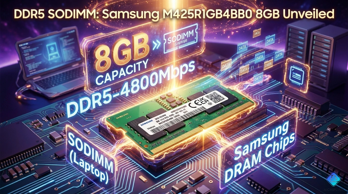
1.0 Full Part Number Decoded: M425R1GB4BB0
Samsung module part numbers encode the product family, form factor, rank, die configuration, die revision, speed grade, and packaging in a structured string:
M — Samsung memory module product prefix (M = module; distinct from K = individual die chip)
4 — Memory technology generation indicator within Samsung's module naming (maps to DDR5 in this series)
25 — Form factor code: 25 = 262-pin SO-DIMM (Small Outline DIMM for laptops and compact systems). Compare: 32 = 288-pin UDIMM (desktop), 32R = 288-pin RDIMM (server).
R — Memory type: R = SDRAM (standard DRAM, not NVDIMM or other specialty type)
1 — Rank count: 1 = Single rank (1R). The entire module serves as one logical memory rank; all chips on the module respond to the same chip-select signal.
GB4 — Die configuration code:
- G = die density tier (maps to 8 Gb per die in this context)
- B = die data width tier (maps to x16 width per die — each die presents 16 data bits)
- 4 = number of die packages on the module (4 dies total)
- Combined: 4 dies × 8 Gb each = 32 Gb total raw; organized as 1024M × 64-bit = 8 GB per module
B — Die revision: B = second die revision within the DDR5 8 Gb x16 product family (first revision was A)
B0 — Speed/revision bin code within the B die family
Ordering suffix (after the dash):
| Suffix | Speed | Timing | Notes |
|---|---|---|---|
| -CQK | DDR5-4800 (PC5-38400) | CL40 | Base speed, most common |
| -CWM | DDR5-5600 (PC5-44800) | CL46 | Higher speed variant |
| -CQKOL | DDR5-4800 | CL40 | OEM-locked variant |
The suffix characters encode: C = commercial temperature; Q/W = speed bin group; K/M = specific timing bin; additional characters for OEM or packaging variants.
2.0 Specifications and What the Numbers Mean
Confirmed specifications from distributor data and Samsung product page:
- Capacity: 8 GB per module
- DDR generation: DDR5
- Speed grade (-CQK): DDR5-4800 (PC5-38400)
- Peak bandwidth: 4,800 MT/s × 8 bytes = 38,400 MB/s (38.4 GB/s) peak per module
- Primary timings (CQK): CL40-39-39-77 (CAS Latency 40, tRCD 39, tRP 39, tRAS 77 cycles)
- Absolute CAS latency: CL40 at 4800 MT/s → tCK = 1/2400 MHz = 0.4167 ns → tCL = 40 × 0.4167 ns = 16.67 ns
- Operating voltage: 1.1V (DDR5 standard — lower than DDR4's 1.2V)
- Form factor: 262-pin SO-DIMM
- Rank configuration: 1Rx16 (single rank, x16 die width)
- Module organization: 1024M × 64-bit
- ECC: Non-ECC (standard consumer/laptop module)
- On-Die ECC: Yes (DDR5 internal feature — see Section 3)
- SPD (Serial Presence Detect): Yes, EEPROM on module for auto-configuration
Speed comparison for the M425R1GB4BB0 family:
| Suffix | Speed | Peak BW | CL | Absolute tCL | VDD |
|---|---|---|---|---|---|
| -CQK | DDR5-4800 | 38.4 GB/s | 40 | 16.67 ns | 1.1V |
| -CWM | DDR5-5600 | 44.8 GB/s | 46 | 16.43 ns | 1.1V |
Note: the absolute CAS latency (in nanoseconds) is similar between the two speeds because the higher data rate runs a faster clock — higher CL number but nearly identical nanosecond latency.
3.0 What Is New in DDR5: Sub-Channels, On-Die ECC, and the VPP Rail
DDR5 is not simply faster DDR4. Several architectural changes affect how it is designed with and how it behaves in the system, and M425R1GB4BB0 implements all of them:
Sub-channel architecture:
DDR4's 64-bit data bus operates as one wide channel. DDR5 splits this into two independent 32-bit sub-channels within a single DIMM slot. Each sub-channel has its own command/address bus, its own data bus, and its own independent operation. The memory controller can issue independent commands to each sub-channel — for example, reading from sub-channel 0 while sub-channel 1 executes a precharge. This sub-channel independence, combined with the higher per-pin data rate, gives DDR5 substantially higher sustained bandwidth than DDR4 at equivalent clock frequencies.
For the M425R1GB4BB0's 4 chips organized as 1Rx16: 2 chips serve sub-channel 0 (each contributing 16 bits = 32 bits total per sub-channel), and 2 chips serve sub-channel 1. The two sub-channels operate independently, enabling the memory controller to pipeline operations across both halves.
On-Die ECC (ODECC):
All DDR5 devices include on-die ECC — a hardware error correction circuit inside each DRAM die that detects and corrects single-bit errors within the die's internal array before the data is sent to the memory bus. This is not the same as system-level ECC (which requires ECC DIMM + ECC-capable memory controller). On-die ECC is transparent to the memory controller and provides data integrity improvement within the die without any change to the external interface. The M425R1GB4BB0 is a Non-ECC module (no extra bits on the module-level data bus), but its internal die-level ODECC operates regardless.
VPP — the new supply rail:
Like DDR4, DDR5 requires a VPP supply rail (2.5V) in addition to VDD/VDDQ (1.1V). This VPP rail was not present in DDR3 or earlier. System designers migrating from DDR4 to DDR5 do not need to add VPP (DDR4 also required it), but designers moving from DDR3 must add this supply rail.
DDR5 additionally introduces an on-DIMM voltage regulator (PMIC — Power Management IC) for server RDIMM applications. SO-DIMMs like M425R1GB4BB0 do not typically include a PMIC; the host platform provides the regulated VDD/VDDQ directly.
4.0 The Real Performance Difference: 1Rx16 vs 2Rx8
This is the most practically significant technical detail about M425R1GB4BB0 that is invisible from the marketing specifications.
What 1Rx16 means physically:
The M425R1GB4BB0 has 4 DDR5 die packages on the PCB. Each die is an x16 device — it contributes 16 data bits to the module's 64-bit bus (2 sub-channels × 32 bits each = 64 bits). All 4 dies share one chip-select signal (one rank). When the memory controller issues a command, all 4 dies respond simultaneously as a single unit.
What 2Rx8 means physically (comparison):
A hypothetical 8GB DDR5 SO-DIMM in 2Rx8 configuration would have 16 die packages — 8 per rank, each contributing 8 bits. The two ranks have independent chip-select signals. The memory controller can address Rank 0 and Rank 1 alternately in a pipelined fashion.
Why rank interleaving matters for bandwidth:
A DRAM row access cycle requires: ACTIVATE (open a row) → CAS READ/WRITE (access columns) → PRECHARGE (close the row). The precharge step takes time — the row cannot be accessed again until it completes. With a single rank, the memory controller must wait for precharge before issuing another row activation to the same bank.
With two ranks, while Rank 0 is precharging, Rank 1 can be activating and reading. The controller can alternate between ranks, keeping the data bus busy during the idle-wait periods. In bandwidth-intensive workloads, this rank interleaving can improve sustained bandwidth by 10–30% compared to a single-rank configuration at the same DDR5 speed grade.
When does 1Rx16 matter in practice?
For most laptop workloads — office applications, web browsing, document editing, moderate gaming — the memory subsystem is rarely bandwidth-limited, and the difference between 1Rx16 and 2Rx8 is not perceptible. For workloads that are genuinely memory-bandwidth bound — video editing with large raw files, machine learning inference, scientific simulation — the 2Rx8 configuration's rank interleaving advantage becomes measurable. For embedded applications using DDR5 SO-DIMM in a single-board computer or industrial compute module where consistent memory throughput matters, verify whether the application workload is bandwidth-bound before specifying 1Rx16 as the lower-cost option.
5.0 Five Misconceptions About This Module
Misconception 1: "GB4 means 4 GB"
The most common misreading. GB4 in Samsung's module naming is a die configuration code — 8 Gb die × 4 packages = 32 Gb = 4 GB per 32-bit half-channel, but 8 GB total across the full 64-bit bus. The full capacity is encoded in the combination of die density (G = 8 Gb), die width (B = x16), and die count (4), organized across the full 64-bit module width. The resulting 8 GB capacity matches the marketing label, but reading "GB4" as "4 GB" misunderstands what each field encodes.
Misconception 2: "DDR5-4800 CL40 has higher latency than DDR4-3200 CL22"
In clock cycles, CL40 > CL22. In absolute time: DDR5-4800 CL40 → tCL = 40/(4800/2) = 40/2400 = 16.67 ns. DDR4-3200 CL22 → tCL = 22/1600 = 13.75 ns. DDR5-4800 has approximately 2.9 ns more first-access latency than DDR4-3200. However, DDR5's dramatically higher bandwidth more than compensates in throughput-bound workloads. For latency-critical workloads (pointer-chasing memory access patterns in databases), this extra 2.9 ns per access is meaningful; for sequential or streaming workloads, the bandwidth advantage of DDR5 dominates.
Misconception 3: "Non-ECC means no error correction in this module"
Non-ECC refers to the system-level ECC interface — the module has no extra bits on its external data bus for system ECC (which would require a 72-bit bus instead of 64-bit, and an ECC-capable memory controller). However, all DDR5 dies include on-die ECC (ODECC) that operates internally within each chip, correcting single-bit errors within the die before data reaches the bus. This internal correction is present in M425R1GB4BB0 regardless of the "Non-ECC" label, and provides a meaningful reliability improvement over DDR4 (which had no on-die ECC). For applications requiring full system-level ECC, an ECC SO-DIMM and ECC-capable platform are still needed.
Misconception 4: "M425R1GB4BB0-CQK and M425R1GB4BB0-CWM can be mixed in a dual-channel system"
The -CQK (DDR5-4800) and -CWM (DDR5-5600) variants are the same die at different speed bins. Mixing them in a dual-channel system (two SO-DIMM slots) forces the memory controller to operate both modules at the lower speed (DDR5-4800). This is functionally acceptable but wastes the CWM's higher speed capability. For optimal performance, use matched pairs in the same speed grade. Matching is more important for dual-channel throughput than absolute speed — two matched CQK modules operating in dual-channel mode will outperform mismatched CQK+CWM running at the lower speed with potential timing inconsistencies.
Misconception 5: "DDR5 SO-DIMM fits in DDR4 SO-DIMM slots"
DDR5 and DDR4 SO-DIMMs have different key notch positions and different pin counts (DDR5: 262 pins; DDR4: 260 pins). DDR5 SO-DIMMs physically cannot be inserted into DDR4 SO-DIMM slots, and vice versa. The different notch position is an intentional mechanical lockout. Attempting to force a DDR5 module into a DDR4 slot risks damaging the module and the slot. Always verify the DDR generation supported by the platform before ordering memory.
6.0 Practice Problems
Problem 1: An M425R1GB4BB0-CQK runs at DDR5-4800 with CL40. What is the actual CAS latency in nanoseconds? Compare to DDR3-1600 CL11. (Answer: DDR5 tCL = 40 / 2400 MHz = 16.67 ns. DDR3 tCL = 11 / 800 MHz = 13.75 ns. DDR5-4800 has ~2.9 ns more first-access latency than DDR3-1600, despite the 3× higher data rate.)
Problem 2: A laptop supports dual-channel DDR5 with two SO-DIMM slots. You install one 8GB M425R1GB4BB0-CQK (1Rx16) and one 16GB DDR5-4800 SO-DIMM (2Rx8). Does this system run in dual-channel mode? (Answer: Depends on the platform. Most modern memory controllers support asymmetric dual-channel (flex mode), where the first 8GB of each module runs in dual-channel, and the remaining 8GB of the 16GB module runs in single-channel. Check the platform's memory configuration guide for the specific behavior.)
Problem 3: What is the peak theoretical bandwidth of two M425R1GB4BB0-CQK modules in a dual-channel DDR5 configuration? (Answer: Each module: 38.4 GB/s. Dual-channel doubles the bus width (2 × 64 bits = 128 bits), so peak bandwidth = 38.4 × 2 = 76.8 GB/s. This compares to ~51.2 GB/s for dual-channel DDR4-3200.)
7.0 Real Questions from System Builders and Engineers
Q: The M425R1GB4BB0-CQK is listed as "1Rx16" but a competing 8GB DDR5 SO-DIMM is listed as "2Rx8." Both are DDR5-4800. Which should I choose for a video editing workstation laptop?
A: For video editing — which involves reading large sequential blocks of compressed video data and writing large output files — memory bandwidth matters more than latency. The 2Rx8 configuration's rank interleaving delivers higher sustained bandwidth in sequential workloads, typically 10–20% higher than 1Rx16 at the same DDR5 speed. If the laptop platform supports both configurations (verify compatibility), the 2Rx8 module will provide measurably better throughput in bandwidth-intensive video editing scenarios. The 1Rx16 (M425R1GB4BB0) is typically lower cost and adequate for general-purpose use; for a dedicated workstation use case, the 2Rx8 variant is the better technical choice if available.
Q: I upgraded my laptop from DDR4-3200 16GB to two M425R1GB4BB0-CQK (16GB total DDR5-4800) and it actually feels slower in some scenarios. How is that possible?
A: The most likely explanation is that you moved from a 2Rx8 or larger DDR4 configuration to 1Rx16 DDR5 — gaining bandwidth in some scenarios but losing rank interleaving that the DDR4 had. Additionally, DDR5's first-access latency (16.67 ns at CL40) is higher than DDR4-3200 (13.75 ns at CL22). For workloads dominated by pointer-chasing (database traversals, some gaming scenarios with large asset streaming), the higher latency is noticeable despite the higher bandwidth. Finally, confirm the system is running in dual-channel mode (two modules installed in the correct slots) — single-channel DDR5 can be slower than dual-channel DDR4 in bandwidth-sensitive workloads.
Q: We are designing an industrial compute module using DDR5 SO-DIMM. Is M425R1GB4BB0-CQK available in industrial temperature grade?
A: The standard M425R1GB4BB0-CQK is rated for commercial temperature (typically 0°C to +85°C case temperature, as is standard for SO-DIMM modules). For industrial temperature requirements (−40°C to +85°C or beyond), Samsung offers specific industrial-grade DDR5 SO-DIMM variants with extended temperature qualification — these typically carry different suffix codes indicating industrial temperature screening. For industrial embedded designs, explicitly request industrial temperature grade SO-DIMMs from Samsung's authorized distribution or engage Samsung Semiconductor's embedded DRAM product line directly. Do not use commercial-temperature SO-DIMMs in applications that experience sub-0°C ambient temperatures without verifying that the platform and memory have been tested and qualified at those temperatures.
8.0 Quick Reference Card
Part Number Decode:
| Field | Value | Meaning |
|---|---|---|
| M | M | Samsung memory module |
| 4 | 4 | DDR5 generation indicator |
| 25 | 25 | 262-pin SO-DIMM |
| R | R | SDRAM type |
| 1 | 1 | Single rank (1R) |
| GB4 | GB4 | 4 × 8Gb x16 dies = 8GB total |
| B | B | Die revision B |
| B0 | B0 | Speed/stepping bin |
Suffix Speed Comparison:
| Suffix | Speed | Timing | Peak BW | Absolute tCL |
|---|---|---|---|---|
| -CQK | DDR5-4800 | CL40 | 38.4 GB/s | 16.67 ns |
| -CWM | DDR5-5600 | CL46 | 44.8 GB/s | 16.43 ns |
1Rx16 vs 2Rx8 — Performance Impact:
| Configuration | Chips | Rank interleaving | BW advantage | Best for |
|---|---|---|---|---|
| 1Rx16 (this module) | 4 × x16 | None | — | General use, cost-optimized |
| 2Rx8 | 16 × x8 | Yes | +10–30% | Bandwidth-intensive workloads |
DDR5 New Features vs DDR4:
| Feature | DDR5 | DDR4 |
|---|---|---|
| Sub-channels | 2 × 32-bit | 1 × 64-bit |
| On-die ECC | Yes (internal) | No |
| VDD/VDDQ | 1.1V | 1.2V |
| Pin count (SO-DIMM) | 262 | 260 |
| Physical compatibility | Not compatible | Not compatible |
The Key Math: GB4 → 8GB 4 dies × 8 Gb/die = 32 Gb ÷ 8 = 4 GB per 32-bit sub-channel × 2 sub-channels = 8 GB total
For sourcing Samsung M425R1GB4BB0 DDR5 SO-DIMM with verified authenticity and competitive pricing, visit aichiplink.com.

Written by Jack Elliott from AIChipLink.
AIChipLink, one of the fastest-growing global independent electronic components distributors in the world, offers millions of products from thousands of manufacturers, and many of our in-stock parts is available to ship same day.
We mainly source and distribute integrated circuit (IC) products of brands such as Broadcom, Microchip, Texas Instruments, Infineon, NXP, Analog Devices, Qualcomm, Intel, etc., which are widely used in communication & network, telecom, industrial control, new energy and automotive electronics.
Empowered by AI, Linked to the Future. Get started on AIChipLink and submit your RFQ online today!
Frequently Asked Questions
What does 1Rx16 mean on the M425R1GB4BB0 module?
1Rx16 means the module uses a single memory rank with x16-wide DDR5 chips. In the M425R1GB4BB0, four x16 DRAM chips combine to create the full 64-bit data bus. Compared with 2Rx8 modules, 1Rx16 designs usually use fewer chips and lower cost, but they may deliver lower sustained bandwidth because they cannot benefit from rank interleaving during heavy workloads like video editing or scientific computing.
Is M425R1GB4BB0 compatible with DDR4 laptops?
No. DDR5 SO-DIMM modules are not physically or electrically compatible with DDR4 slots. The M425R1GB4BB0 uses a 262-pin DDR5 SO-DIMM layout operating at 1.1V, while DDR4 SO-DIMMs use 260 pins and different signaling. The notch position is also different to prevent incorrect installation.
What is the difference between M425R1GB4BB0-CQK and M425R1GB4BB0-CWM?
The main difference is speed grade and timing. The -CQK version operates at DDR5-4800 CL40, while the -CWM version supports DDR5-5600 CL46. Although the CL number is higher on the faster module, the actual latency in nanoseconds is nearly the same because DDR5-5600 runs at a higher clock frequency. Systems mixing both versions usually downclock to the slower DDR5-4800 speed.
Does this module support ECC memory protection?
The M425R1GB4BB0 is a Non-ECC consumer SO-DIMM, but it still includes DDR5 on-die ECC internally. On-die ECC corrects errors inside each DRAM chip and improves reliability compared with DDR4. However, it does not provide full system-level ECC protection because the module lacks the additional ECC data bits required by workstation or server platforms.
Is M425R1GB4BB0 good for upgrading modern laptops?
Yes, if the laptop officially supports DDR5-4800 SO-DIMM memory. The module provides 8GB capacity, low 1.1V power consumption, and up to 38.4 GB/s peak bandwidth. It works well for office productivity, web browsing, programming, and general laptop upgrades. For high-end workstation or gaming systems, users may prefer larger-capacity 2Rx8 DDR5 modules for improved sustained memory throughput.