What Is SBAS70-04LT1G? Two Characters in the Part Number That Both Need Explanation
The SBAS70-04LT1G part number has two elements that are easy to misread and both matter for selection:
The S at the beginning is not simply a product series initial. In onsemi's naming convention, the S prefix on a device that already exists without it (BAS70-04LT1G is the commercial version) indicates that the device is manufactured with unique site and control change requirements — a supply chain traceability designation for automotive and other applications requiring controlled process changes. This is what enables AEC-Q101 qualification and PPAP documentation support. An engineer specifying SBAS70-04LT1G for a non-automotive design is paying for automotive-grade qualification and supply chain controls they may not need. An engineer specifying BAS70-04LT1G for an automotive design is accepting a component that may not have the required process documentation — even if the electrical specifications are identical.
The 04 in BAS70-04 encodes the internal diode configuration. This is the field that determines how the two Schottky junctions inside the SOT-23-3 package are interconnected. 04 = dual series — the two diodes are connected anode-to-cathode in series, so the combination blocks up to 140V (2 × 70V) rather than 70V from a single junction. Other BAS70 variants use the same junctions but arrange them differently: 03W is dual common-cathode (both cathodes tied to one pin, the "or-ing" configuration), 05 is dual common-anode. Choosing 04 when you need 03W gives a component that does not perform its intended function, despite being in the same package with the same electrical measurements on individual junctions.
These two characters determine, respectively, whether the part meets automotive qualification requirements and whether the internal circuit topology matches the application. Both are worth understanding before placing an order.
1.0 Full Part Number Decoded: SBAS70-04LT1G
S — Automotive supply chain prefix: In onsemi's product naming, the S prefix indicates the device is manufactured with site and process change control requirements beyond the standard commercial product. This enables:
- AEC-Q101 qualification (automotive semiconductor qualification standard)
- PPAP (Production Part Approval Process) documentation capability
- Change notification per IATF 16949 / automotive supplier quality requirements
The non-S version (BAS70-04LT1G) is electrically identical but manufactured without the automotive supply chain controls.
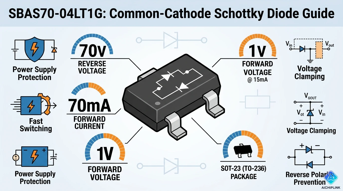
BAS70 — Product family: BAS = Small Signal Schottky Barrier Diode family; 70 = 70V maximum repetitive reverse voltage rating
-04 — Internal circuit configuration:
- -04 = Dual Series — two Schottky diodes connected anode-to-cathode in series within one package (total blocking voltage: 2 × 70V = 140V effective)
- -03W = Dual Common-Cathode — both cathodes tied together (ideal OR-ing diode, voltage selector, or dual independent ESD clamp)
- -05 = Dual Common-Anode — both anodes tied together
L — Package variant: L = SOT-23 with specific lead forming and tape-and-reel orientation optimized for automated placement
T1G — Packaging:
- T = Tape-and-reel
- 1 = 3,000 units per reel (standard volume packaging)
- G = RoHS compliant, lead-free (Pb-free) terminal finish
2.0 Specifications
From the onsemi BAS70-04L / SBAS70-04L datasheet (Rev. 7):
Voltage ratings:
- VRRM (Repetitive Reverse Voltage, per junction): 70V maximum
- VR (Total series stack blocking voltage): 140V effective (2 × 70V in series)
- VF (Forward Voltage, per junction): 0.41V typical at IF = 1 mA (25°C); 1.0V maximum at IF = 70 mA
Current ratings:
- IF (Continuous Forward Current, per diode): 70 mA maximum
- IFSM (Forward Surge Current): 100 mA maximum (non-repetitive)
- IR (Reverse Leakage Current): 2 µA maximum at VR = 70V (25°C); significantly higher at elevated temperature — see Section 6
Switching performance:
- trr (Reverse Recovery Time): Not specified — Schottky diodes have no minority carrier storage, so trr is in the picosecond range (essentially zero) rather than the nanosecond range of PN diodes
Thermal:
- TJ (Junction Temperature) max: 150°C
- TSTG (Storage Temperature): −65°C to +150°C
- PD (Power Dissipation): 250 mW (SOT-23, TA = 25°C, derate 2.0 mW/°C above 25°C)
- θJA (Thermal Resistance, junction-to-ambient): 500°C/W (SOT-23, no heatspreading)
Package:
- SOT-23-3 (TO-236-3, SC-59), surface mount
- Marking code: CG (date code added separately)
- Tape-and-reel: 3,000 units per reel
Qualification:
- AEC-Q101 qualified (SBAS70 variant)
- PPAP capable (SBAS70 variant)
- RoHS 3 compliant
3.0 The Physics: Why Schottky Is Different from a PN Diode
The critical difference between a Schottky diode and a standard silicon PN junction diode is not the lower forward voltage drop — that is the consequence, not the cause. The fundamental difference is the absence of minority carrier storage.
How a PN diode works — and what creates its speed limitation:
In a standard PN junction diode, electrons from the N-type region and holes from the P-type region diffuse across the junction and recombine. When the diode is forward biased, the junction is flooded with minority carriers — electrons on the P-side and holes on the N-side. These minority carriers are stored in the junction region and the depletion layer.
When the diode is reverse-biased (turned off), these stored minority carriers must be swept out before the diode can block reverse current. The time required for this minority carrier sweep-out is the reverse recovery time (trr) — typically 4–200 nanoseconds for small-signal silicon PN diodes. During this recovery interval, the diode conducts significant reverse current (the "reverse recovery spike"), which can cause interference in high-frequency circuits and power loss in switching converters.
How a Schottky diode works — and why there is no recovery time:
A Schottky diode is formed by a metal-semiconductor junction rather than a P-N semiconductor junction. When the Schottky junction is forward biased, current flows by majority carrier injection — electrons from the N-type semiconductor flow into the metal, where they become part of the bulk metal electron sea and do not need to recombine with holes. There are no minority carriers involved and therefore no minority carrier storage.
When the Schottky diode is reverse biased, there are no stored minority carriers to sweep out. The diode turns off in picoseconds — limited only by the RC time constant of the junction capacitance and circuit impedance, not by carrier recombination. This is why Schottky diodes are specified for high-frequency rectifiers, fast-switching protection circuits, and RF detector circuits where nanosecond-scale switching matters.
The lower forward voltage (typically 0.2–0.5V for a Schottky vs 0.6–0.7V for silicon PN at equivalent current) is a direct consequence of the metal-semiconductor contact physics: the potential barrier at a metal-semiconductor interface is lower than at a P-N junction of the same semiconductor material.
The tradeoff — reverse leakage:
The metal-semiconductor junction that enables fast switching also permits more reverse current to flow than a PN junction at the same reverse voltage. The Schottky reverse leakage current approximately doubles for every 10°C rise in temperature (a general rule for semiconductor leakage). At 125°C junction temperature, the reverse leakage of a 70V Schottky may be 100–1,000× higher than at 25°C — potentially reaching hundreds of microamps. For the SBAS70-04LT1G, the 2 µA maximum at 25°C may be 200 µA or more at 125°C at rated voltage. This makes Schottky diodes unsuitable for applications requiring very low reverse leakage at high temperatures.
4.0 Real Circuit Applications: When the Dual-Series Configuration Is the Right Choice
Why use dual-series (04 configuration) at all?
Two Schottky diodes in series provide a total blocking voltage of 2 × 70V = 140V, which is useful when:
- A single 70V Schottky does not provide adequate reverse voltage margin in the circuit
- The application needs a voltage clamp that only activates above a specific threshold that equals two forward voltages (~0.8–1.0V total) — the series stack requires double the voltage to conduct versus a single diode
Common applications of the dual-series BAS70-04 / SBAS70-04:
Overvoltage clamping with higher threshold: A single Schottky starts conducting at approximately 0.3–0.5V forward. In a circuit where any forward conduction would affect signal quality, two series diodes provide 0.6–1.0V of "dead band" before clamping occurs — useful in signal protection circuits where the normal operating voltage is in the 0.5–0.9V range.
High-voltage transient suppression in two-stage protection: Paired with a TVS diode or Zener, the dual-series Schottky stack provides a fast initial clamping element for very fast transients (nanosecond rise time, where Schottky's fast recovery matters) ahead of a slower but more energy-capable TVS. The series stack's 140V limit provides a higher voltage capability than a single 70V device.
Detector and mixer circuits in RF front-ends: RF detectors in receivers use Schottky diodes for their fast switching and low forward voltage. A series-connected pair allows the detector to operate over a wider voltage range before the diode saturates.
When to use the -03W (common-cathode) instead:
The BAS70-03W configuration (both cathodes tied to pin 2, anodes at pins 1 and 3) is used when two independent Schottky diodes with shared cathode are needed — for example, a voltage OR-ing circuit where the higher of two input voltages is selected. This configuration is electrically distinct from -04 and cannot be substituted.
When to use the -05 (common-anode) instead:
The BAS70-05 (both anodes at the middle pin) is used for dual-cathode clamping, where two signals are each clamped to a reference voltage through the shared anode.
5.0 Five Misconceptions About Schottky Diodes and This Part
Misconception 1: "SBAS70-04LT1G and BAS70-04LT1G are interchangeable"
Electrically they are identical. The S prefix adds automotive supply chain traceability and AEC-Q101 qualification — not different silicon, not different electrical performance. In an automotive application where the quality management system requires AEC-Q101 qualified components and PPAP documentation, SBAS70-04LT1G is required and BAS70-04LT1G is not compliant regardless of matching electrical specs. In a consumer electronics application with no such quality requirements, BAS70-04LT1G provides identical performance at potentially lower cost. The choice is determined by application quality requirements, not electrical needs.
Misconception 2: "The dual-series configuration blocks 70V in both directions"
Dual-series means the two diodes are oriented the same way (anode→cathode→anode→cathode through the package), not opposing. In the forward direction, both diodes conduct at approximately double the single-diode forward voltage. In the reverse direction, both diodes block, providing 2 × 70V = 140V total blocking. The configuration does not provide bidirectional blocking — for bidirectional voltage clamping, an anti-parallel configuration or a different device type (bidirectional TVS) is needed.
Misconception 3: "Schottky diodes are always better than PN diodes because of lower forward voltage"
The lower forward voltage is advantageous in power rectification (reduces conduction loss), but Schottky diodes have higher reverse leakage current that increases dramatically with temperature. In a high-temperature application (automotive engine bay, industrial high-temperature enclosure) at 125–150°C junction temperature, a Schottky's reverse leakage may be orders of magnitude higher than a PN junction's, causing circuit malfunction. For applications requiring very low leakage at high temperature, a PN junction diode is preferable despite its higher forward voltage.
Misconception 4: "Zero reverse recovery time means Schottky can be used at any frequency"
The switching speed of a Schottky diode in a real circuit is limited not only by carrier recovery (which is indeed near-zero) but also by the junction capacitance (CJ). At zero bias, CJ for the SBAS70-04LT1G is approximately 2–5 pF per junction. At high frequencies, this capacitance shunts the junction and allows AC signals to pass even in the "off" state. At RF frequencies (hundreds of MHz to GHz), the junction capacitance becomes a significant impedance, and the diode's isolation in the reverse direction degrades. The effective high-frequency limit depends on the specific circuit impedances, but junction capacitance always creates an upper frequency bound.
Misconception 5: "VF = 0.41V means the forward voltage drop is always about 0.41V"
The 0.41V typical is measured at IF = 1 mA and TA = 25°C. The actual forward voltage has significant dependence on both current and temperature. At IF = 70 mA (rated maximum), VF may be 0.8–1.0V — substantially higher. At elevated temperatures, VF decreases (negative temperature coefficient, approximately −1.0 to −2.0 mV/°C for Schottky diodes) — which means a Schottky diode running hot conducts more easily, which makes it run hotter, a mild positive feedback. In power dissipation calculations, use the VF at the actual operating current and temperature, not the 1 mA / 25°C test condition value.
6.0 Design Notes: VF Temperature Dependence, Leakage, and PCB
Forward voltage temperature coefficient:
Schottky diodes have a negative VF temperature coefficient — as junction temperature increases, VF decreases. For the BAS70 series, VF decreases approximately 1.0–1.5 mV/°C. This matters in two ways:
First, in a power budget calculation for a conduction loss estimate: use VF at the expected operating temperature, not the 25°C datasheet value. A Schottky running at 100°C has VF approximately 100 × 1.2 mV = 120 mV lower than at 25°C — at 0.41V typical at 1 mA, the hot value is approximately 0.29V. This reduces conduction loss but also means the clamping threshold (for protection applications) is lower at high temperature.
Second, in thermal design: the reduced VF at high temperature means a Schottky handling significant current dissipates slightly less power as it heats up (self-compensating behavior), which is the opposite of some power devices that can thermal runaway.
Reverse leakage at elevated temperature:
The reverse leakage current approximately doubles per 10°C increase in junction temperature for the Schottky junction. Starting from 2 µA at 25°C and 70V:
- At 75°C: ~64 µA
- At 125°C: ~2,000 µA (2 mA)
At 2 mA reverse leakage, the power dissipated at 70V reverse voltage is 140 mW — more than half the device's rated 250 mW total dissipation. This severely limits the usable operating range at high temperature and high reverse voltage simultaneously. For the SBAS70-04LT1G in automotive applications (−40°C to +125°C), the reverse leakage at the maximum junction temperature must be included in the power budget.
PCB layout for SOT-23-3:
The SOT-23-3 package (2.9 mm × 1.3 mm body) is small enough that PCB thermal relief is typically not needed or desirable — the copper pads and traces serve as the primary heat path. Pad dimensions per JEDEC SOT-23 land pattern (approximately 1.0 mm × 0.8 mm per pad). For protection applications where the diode handles surge currents, ensure the pad-to-via copper path can handle the surge current without excessive resistive voltage drop — use solid copper fills rather than thin traces between the pad and the connecting via.
7.0 Real Questions from Circuit Designers
Q: I am using SBAS70-04LT1G for reverse polarity protection on a 12V input in an automotive design. Is 70V (or 140V series) sufficient margin?
A: For a 12V nominal automotive supply, the relevant voltage stress is the load dump transient — a spike that can reach 40–60V transiently when the alternator load is suddenly removed (defined in ISO 7637-2 and ISO 16750-2). A single 70V Schottky provides barely adequate margin for a 60V load dump peak; in practice, automotive designers use a 70V Schottky for series protection only when followed by a TVS or suppression capacitor to handle the load dump energy, since the Schottky absorbs the initial fast transient while the TVS handles the sustained overvoltage energy. The dual-series 140V rating of SBAS70-04LT1G provides more comfortable load dump margin and may simplify the protection network. However, verify that the 70 mA continuous current rating is adequate for the reverse polarity path — for higher currents, a MOSFET-based reverse polarity protection circuit is more appropriate than a series diode.
Q: Can SBAS70-04LT1G be used as a fast rectifier in a 70V DC-DC converter running at 1 MHz? What is the actual switching speed limitation?
A: The absence of minority carrier reverse recovery makes Schottky diodes in principle suitable for high-frequency rectification. The limiting factor at 1 MHz is the junction capacitance. At 70V reverse voltage, the junction capacitance of a BAS70-series diode is approximately 0.5–1 pF (voltage-dependent, decreasing as reverse voltage increases). At 1 MHz, the capacitive impedance is 1/(2π × 10⁶ × 1 × 10⁻¹²) = approximately 159 kΩ — very high, so capacitive bypass is not a concern at 1 MHz. The diode will function as a fast rectifier at 1 MHz with negligible switching loss from reverse recovery or capacitive effects. At 100 MHz, the same capacitance presents 1.6 kΩ — at this frequency, the capacitive shunting begins to matter if the signal source impedance is in a similar range. For 1 MHz rectification at 70V and 70 mA, SBAS70-04LT1G is technically viable, but verify that the 250 mW power dissipation rating is adequate for the combined forward conduction and capacitive switching losses at 1 MHz.
Q: We specified BAS70-04LT1G for our initial prototype — now the automotive customer is requesting AEC-Q101 qualified parts. Do we need to requalify the circuit if we switch to SBAS70-04LT1G?
A: The SBAS70-04LT1G uses the same die fabricated on the same production line as BAS70-04LT1G, with the addition of the automotive supply chain controls (site change notification, process change control, PPAP documentation). Electrically, they are characterized to the same specifications. In most automotive qualification frameworks (IATF 16949, customer-specific requirements), substituting an equivalent or more rigorously qualified component (SBAS for BAS) in the same package does not require full re-qualification of the circuit — it requires documentation of the component change in the design change management process and verification that the substitute meets or exceeds all specifications of the original. The specific requirement depends on your customer's quality management requirements and whether the design is in a confirmed/frozen status. Consult with your customer's quality team before assuming the substitution is automatic.
8.0 Quick Reference Card
Part Number Decode:
| Field | Value | Meaning |
|---|---|---|
| S | S | Automotive supply chain (AEC-Q101, PPAP) |
| BAS70 | BAS70 | 70V small-signal Schottky family |
| -04 | -04 | Dual Series configuration |
| L | L | SOT-23 package variant |
| T1 | T1 | Tape-and-reel, 3,000/reel |
| G | G | RoHS compliant, lead-free |
Key Specifications:
| Parameter | Value |
|---|---|
| VRRM (per junction) | 70V |
| Effective blocking (series) | 140V |
| IF max (continuous) | 70 mA |
| IFSM (surge) | 100 mA |
| VF typical @ 1 mA | 0.41V |
| VF max @ 70 mA | 1.0V |
| IR max @ 25°C | 2 µA (70V) |
| TJ max | 150°C |
| PD max | 250 mW (25°C, derate 2 mW/°C) |
| Package | SOT-23-3 (TO-236) |
| Qualification | AEC-Q101 |
BAS70 Configuration Family:
| Suffix | Config | Topology | Use case |
|---|---|---|---|
| -04 | Dual Series | A→K→A→K | Higher blocking voltage, dual-VF threshold |
| -03W | Dual Common-Cathode | A₁→K←A₂ | OR-ing, dual ESD clamp, voltage select |
| -05 | Dual Common-Anode | K₁←A→K₂ | Dual cathode clamping |
Why Schottky (not PN) for fast switching:
PN diode: Minority carriers stored → reverse recovery time 4–200 ns → switching loss at high frequency
Schottky: No minority carriers → reverse recovery ≈ 0 → limited only by junction capacitance (picoseconds to nanoseconds)
The Two Temperature Tradeoffs:
| Parameter | As temperature rises | Impact |
|---|---|---|
| VF | Decreases (~1.2 mV/°C) | Lower conduction loss; lower clamp threshold |
| IR | Increases exponentially (~2× per 10°C) | Major issue at high T + high reverse voltage |
SBAS vs BAS — when each applies:
- SBAS70-04LT1G: Automotive designs, AEC-Q101 required, PPAP documentation needed
- BAS70-04LT1G: Consumer electronics, industrial non-automotive, cost-optimized designs
For sourcing onsemi SBAS70-04LT1G with verified authenticity and competitive pricing, visit aichiplink.com.

Written by Jack Elliott from AIChipLink.
AIChipLink, one of the fastest-growing global independent electronic components distributors in the world, offers millions of products from thousands of manufacturers, and many of our in-stock parts is available to ship same day.
We mainly source and distribute integrated circuit (IC) products of brands such as Broadcom, Microchip, Texas Instruments, Infineon, NXP, Analog Devices, Qualcomm, Intel, etc., which are widely used in communication & network, telecom, industrial control, new energy and automotive electronics.
Empowered by AI, Linked to the Future. Get started on AIChipLink and submit your RFQ online today!
Frequently Asked Questions
What is SBAS70-04LT1G and what is it used for?
SBAS70-04LT1G is an AEC-Q101 qualified dual-series Schottky diode in a SOT-23 package designed for high-speed switching, protection, and signal applications. It integrates two Schottky junctions in series to provide higher voltage blocking capability (up to 140V total), making it suitable for automotive circuits, RF detection, ESD protection, and fast transient clamping.
What does the “-04” configuration mean in SBAS70-04LT1G?
The “-04” suffix indicates a dual-series internal configuration, where two Schottky diodes are connected in series inside one package. This arrangement doubles the effective reverse voltage capability compared to a single diode and increases the forward conduction threshold, which is useful for higher-voltage protection and controlled clamping applications.
What is the difference between SBAS70-04LT1G and BAS70-04LT1G?
The key difference is qualification level, not electrical performance. SBAS70-04LT1G includes automotive-grade manufacturing controls, AEC-Q101 qualification, and PPAP support, while BAS70-04LT1G is the commercial-grade version. Both share the same electrical characteristics, but only the SBAS variant meets automotive reliability and traceability requirements.
Why are Schottky diodes like SBAS70-04LT1G faster than PN diodes?
Schottky diodes switch faster because they use majority carriers and have no reverse recovery time. Unlike PN diodes, which store charge and require nanoseconds to turn off, Schottky diodes eliminate this delay, enabling near-instant switching. This makes them ideal for high-frequency circuits, RF applications, and fast protection paths.
What are the main limitations of SBAS70-04LT1G in circuit design?
The main limitations are low current handling and high reverse leakage at elevated temperatures. With a maximum forward current of 70 mA and increasing leakage current as temperature rises, the device is not suitable for power rectification or high-temperature precision circuits. Designers must also consider its junction capacitance in high-frequency applications and ensure proper thermal and voltage margins.