Introduction
Mobile computing has spent the past decade in a relentless pursuit of more memory bandwidth and capacity in ever-shrinking packages. Every generation of smartphone, tablet, and embedded computing platform demands a DRAM solution that simultaneously delivers higher data rates, larger capacity, lower power consumption, and smaller physical footprint — four requirements that pull in different directions and demand sophisticated engineering to satisfy simultaneously. LPDDR3 solved this challenge for the mainstream mobile market from 2013 through 2019, and devices built on LPDDR3 continue to be designed in and deployed across industrial, automotive, and IoT platforms where cost, power envelope, and ecosystem maturity matter as much as raw bandwidth.
The NT6CL512T32AM-H1 from Nanya Technology Corporation is a 16Gb (gigabit) Dual-Die Package (DDP) LPDDR3 SDRAM — two 8Gb dies stacked within a single 178-ball FBGA package — operating at up to 1866 Mbps per pin on a ×32 data bus, with a HSUL_12 interface running from a 1.2 V core supply. It combines the density of a 16Gb component with the compact footprint and low-voltage operation that define LPDDR3 as a standard for power-efficient mobile and embedded memory.
According to JEDEC JESD209-3 (LPDDR3 Standard), LPDDR3 remains the reference design point for mobile DRAM in platforms requiring backward compatibility with existing AP memory controllers, established supply chains, and proven signal integrity solutions — particularly in industrial and automotive segments where LPDDR4 controller support may not be available in the target application processor.
1.0 What Is the NT6CL512T32AM-H1? An Overview
The NT6CL512T32AM-H1 is Nanya Technology's 16Gb, ×32-wide, 1866 Mbps LPDDR3 SDRAM in a 178-ball FBGA package targeting mobile and embedded computing applications. It represents the DDP (Dual Die Package) configuration of Nanya's NT6CL-AM LPDDR3 product line — two 8Gb dies (each organized as 256M × 32) stacked and connected within one package body, presenting a unified 512M × 32 interface to the memory controller.
Decoding the part number:
- NT — Nanya Technology manufacturer prefix
- 6C — LPDDR3 SDRAM product family (Nanya's 6C generation)
- L — Low-power designation (LPDDR)
- 512 — 512 Megaword depth (512M × 32 = 16Gb total)
- T — DDP (Twin/Dual Die Package) configuration; contrast with M (mono/single die)
- 32 — ×32 data bus width (DQ0–DQ31)
- A — Die revision A
- M — 178-ball FBGA package (M = 178-Ball FBGA)
- H1 — Speed grade: 1866 Mbps data rate, Read Latency (RL) = 14 at 1866 Mbps
The companion part NT6CL512T32AM-H0NA is the automotive-extended-temperature variant (−30°C to +105°C — same as the H1 commercial variant for this family). The -H1-TR suffix on some distributor listings denotes tape-and-reel packaging.
"The NT6CL512T32AM-H1 is a 16Gb DDP LPDDR3 SDRAM organized as 512M × 32, operating at 1866 Mbps data rate with RL14. The device uses a HSUL_12 interface with VDD1 = 1.8V and VDD2/VDDQ/VDDCA = 1.2V." — Nanya Technology NT6CL512T32AM-H1 Product Page
2.0 Full Technical Specifications & LPDDR3 Architecture
2.1 Core Density, Speed, and Electrical Parameters
The following parameters are drawn from the Nanya NT6CL512T32AM-H1 datasheet (Rev. 1.6, February 2019):
- Density: 16Gb (16,384 Mb) total; 512M × 32 organization
- Die Configuration: DDP (Dual Die Package) — 2× 8Gb (256M × 32) dies per package
- Data Bus Width: ×32 (DQ0–DQ31); organized as two independent 16-bit channels internally (per LPDDR3 CA bus architecture)
- Data Rate: 1866 Mbps per pin (DDR; effective clock = 933 MHz)
- Minimum Clock Cycle Time (tCK): 1.07 ns
- Read Latency (RL): 14 cycles at 1866 Mbps (Set A); RL = 16 available (Set B)
- Write Latency (WL): 8 cycles at RL14
- Burst Length (BL): BL8 only (fixed per LPDDR3 standard)
- Prefetch: 8n (8 bits prefetched per DQ pin per access cycle)
- Number of Banks: 8 banks per die (16 banks total across DDP)
- Internal Bank Groups: Not applicable (LPDDR3 uses 8-bank flat architecture, no bank groups)
- Row Address Bits: 16 (A0–A15)
- Column Address Bits: 10 (CA bus encoded)
- CA Bus: 10-bit Command/Address bus, double-data-rate (DDR CA)
- Refresh: Auto Refresh (REF) and Self Refresh (SR); Temperature Compensated Self Refresh (TCSR) supported
- tRFC (Refresh Cycle Time): 210 ns (8Gb per die) — critical for scheduling; higher than single-die LPDDR3 8Gb at same density
- tREFI (Refresh Interval): 3.9 µs (standard); 1.95 µs at elevated temperature (> 85°C)
- Operating Temperature: −30°C to +105°C (Commercial/Mobile grade)
- Package: 178-ball FBGA, 9 mm × 12 mm body, 0.65 mm ball pitch
- RoHS / Halogen-Free: Yes
- JEDEC Compliance: JESD209-3 (LPDDR3)
2.2 HSUL_12 Interface and Power Supply Domains
LPDDR3 uses the HSUL_12 (High-Speed Unterminated Logic, 1.2V) interface — a single-ended I/O standard designed for very low power at high data rates. Unlike DDR4's POD12 or DDR3's SSTL15, HSUL_12 does not rely on external termination resistors on the data bus (termination is handled on-die via ODT). The NT6CL512T32AM-H1 has four independent power supply domains:
- VDD1: 1.70 V to 1.95 V (nominal 1.8 V) — powers the core logic and internal row/column decoders
- VDD2: 1.14 V to 1.30 V (nominal 1.2 V) — powers the I/O output drivers
- VDDQ: 1.14 V to 1.30 V (nominal 1.2 V) — powers the data I/O termination circuits and DQ signal levels
- VDDCA: 1.14 V to 1.30 V (nominal 1.2 V) — powers the Command/Address (CA) bus receivers
In practice, VDD2, VDDQ, and VDDCA are typically tied to the same 1.2 V regulated supply rail on the PCB, while VDD1 requires a separate 1.8 V supply. This dual-supply architecture (1.8 V core + 1.2 V I/O) is a defining characteristic of LPDDR3 and requires two separate, well-decoupled power rails from the system's power management IC (PMIC).
Power consumption (representative values):
- Active read/write (IDD4R / IDD4W): ~200–300 mA total from VDD1 + VDD2 at 1866 Mbps, full bus utilization
- Active idle (IDD3N): ~80–100 mA
- Self Refresh (IDD6): ~2–5 mA (TCSR mode, both dies) — very low; defines the standby power budget
- Deep Power Down (IDD8): < 1 µA per die — the absolute minimum power state; all data is lost
2.3 ZQ Calibration, ODT (RTT), and Drive Strength (RON)
The NT6CL512T32AM-H1 supports the full LPDDR3 signal integrity feature set for configurable output impedance and on-die termination:
ZQ Calibration: The ZQ pad connects to an external 240 Ω ±1% precision resistor to GND. Periodic ZQ calibration commands (ZQCL at initialization, ZQCS during operation) adjust the internal pull-up and pull-down driver impedances to maintain calibrated output strength and ODT resistance despite temperature and voltage drift. The 240 Ω ZQ reference resistor must be a 1% tolerance thin-film type placed within 25 mm of the ZQ ball on the PCB.
Drive Strength (RON) options — programmable via Mode Register (MR3):
- 34.3 Ω (pull-down) / 40 Ω (pull-up) — PD34.3_PU40
- 40 Ω / 48 Ω — PD40_PU48
- 34.3 Ω / 48 Ω — PD34.3_PU48
- Single values: 34.3 Ω, 40 Ω, 48 Ω, 60 Ω, 80 Ω
On-Die Termination (ODT / RTT) options — programmable via MR11:
- RTT = 120 Ω
- RTT = 240 Ω
- RTT = disabled (Hi-Z) — the default for LPDDR3 read operations
LPDDR3 ODT is dynamic — it activates only during write operations (as directed by the memory controller's ODT signal) and is disabled during reads, reducing power consumption. Unlike DDR4 where multiple RTT registers provide layered termination, LPDDR3 uses a simpler ODT scheme where the controller asserts ODT on the DQ/DQS lines during write cycles to absorb reflections.
2.4 Key Timing Parameters: tRFC, tREFI, and 8n Prefetch
The 8n prefetch architecture of LPDDR3 means that each read or write command accesses 8 consecutive bits per DQ pin internally — an 8-bit-wide burst of data at the DRAM core level, delivered as 8 DDR transfers on the DQ pins (4 rising + 4 falling clock edges). For a ×32 device like the NT6CL512T32AM-H1, each BL8 read or write transfers:
8 transfers × 32 DQ pins = 256 bits = 32 bytes per access
At 1866 Mbps, each bit transfer takes 1/1866MHz = 0.536 ns. A full BL8 burst completes in 4 clock cycles (8 transfers at DDR = 4 clock cycles): 4 × 1.07 ns = 4.28 ns per burst — enabling extraordinarily high peak bandwidth.
Peak theoretical bandwidth:
BW = Data Rate × Bus Width / 8 = 1866 Mbps × 32 bits / 8 = 7,464 MB/s (≈7.5 GB/s)
tRFC (Refresh Cycle Time): For the 8Gb die within the DDP, tRFC = 210 ns — the time required to complete a single auto-refresh cycle during which the refreshed bank is unavailable. At a tREFI of 3.9 µs, refresh events consume 210/3900 = 5.4% of total bus time — a non-negligible overhead in bandwidth-critical applications. Fine Granularity Refresh (FGR) is not part of the LPDDR3 standard, making refresh overhead management an important consideration in real-time applications.
tREFI at elevated temperature (> 85°C): The TCSR (Temperature Compensated Self Refresh) feature automatically doubles the refresh rate (halves tREFI to 1.95 µs) when the on-die temperature sensor detects junction temperature above 85°C, preventing data retention failures in hot environments at the cost of increased refresh power.
3.0 System Design and Application Contexts
3.1 Smartphone and Tablet Application Processor Memory
The NT6CL512T32AM-H1 is positioned for mobile application processor (AP) memory subsystems in mid-range smartphones, tablets, and compact computing platforms. Major application processors with LPDDR3 support include ARM Cortex-A series platforms from Qualcomm (Snapdragon 4xx, 6xx series), MediaTek (MT6xxx Helio series), and Rockchip (RK3288, RK3399). In these designs, the NT6CL512T32AM-H1 provides 2 GB of working memory (16Gb ÷ 8 bits/byte = 2 GB) on a single ×32 channel.
The 1866 Mbps data rate delivers 7.5 GB/s peak bandwidth on a single ×32 LPDDR3 channel — sufficient for:
- 1080p/4K video decode and encode pipelines
- Android OS and application workloads requiring 2 GB of physical RAM
- GPU workloads in mobile SoCs (frame buffer, texture cache)
- Camera ISP (Image Signal Processor) working buffers for multi-frame HDR processing
For designs requiring 4 GB of total memory, two NT6CL512T32AM-H1 devices in a dual-channel ×64 configuration (if the AP supports dual-channel LPDDR3) doubles both capacity and bandwidth to 15 GB/s theoretical peak.
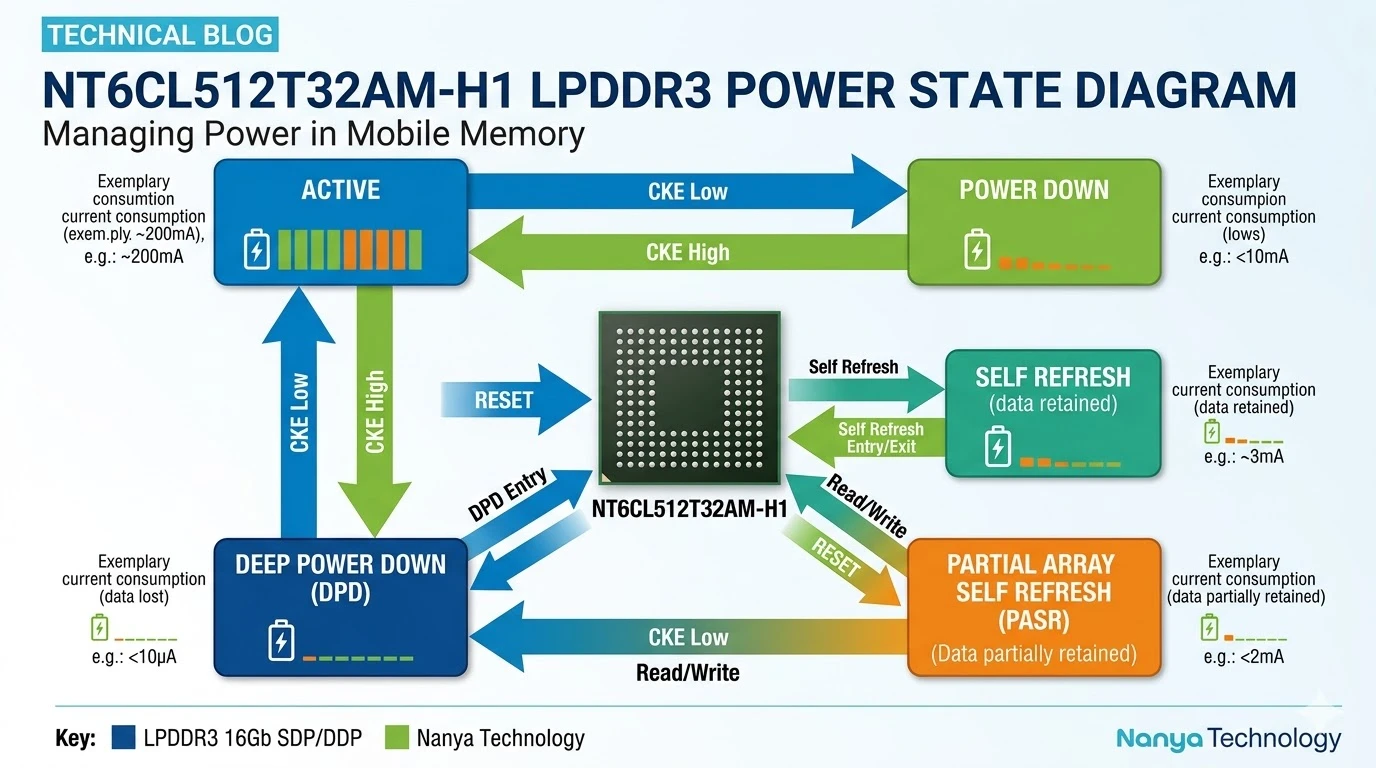
3.2 Power-Saving Modes: DPD, PASR, TCSR, and Clock Stop
The NT6CL512T32AM-H1 implements the complete LPDDR3 power management hierarchy — essential for extending battery life in mobile devices where memory power is a significant fraction of total platform power:
Clock Stop: During idle periods (no active command in progress), the memory controller can hold the CK/CK_n differential clock pair static (both low) to eliminate switching current in the DRAM's clock tree. Clock can be stopped at any time when the bank is precharged and the device is idle. This is the lowest-overhead power saving mechanism — no state is lost and the device resumes normal operation immediately upon clock restart.
Power Down Mode: When all banks are precharged and the CKE (Clock Enable) signal is deasserted (CKE = LOW), the DRAM enters Power Down mode. DLL (Delay-Locked Loop) is disabled, reducing current to IDD2P level. Data is retained. The device exits Power Down within tXP after CKE is reasserted.
Self Refresh (SR): The DRAM autonomously manages its own refresh operations, allowing the memory controller to completely shut down its clock and power-save circuits while the DRAM retains all data. Self Refresh current (IDD6) of ~2–5 mA total is the dominant memory power consumption in smartphone deep sleep states. TCSR (Temperature Compensated Self Refresh) automatically increases the refresh rate at elevated temperatures to maintain data integrity without controller intervention.
Partial Array Self Refresh (PASR): Configures the DRAM to only refresh a user-defined subset of its banks during Self Refresh — for example, only 2 of 8 banks. Banks that are not refreshed lose their data, but if the system can guarantee those banks contain no critical data during sleep, PASR reduces Self Refresh power proportionally. At PASR = 1/8 (one bank retained), Self Refresh current may drop to ~0.5–1 mA — a significant improvement for ultra-long standby applications.
Deep Power Down (DPD): The absolute minimum power state — the DRAM shuts down all internal circuits including the voltage regulators and refresh logic. Current drops to < 1 µA per die, but all data is lost. DPD is used when the system undergoes a complete power-off sequence and DRAM content will be reloaded from non-volatile storage upon wake-up.
3.3 Embedded Computing and Industrial Mobile Platforms
Beyond consumer smartphones and tablets, the NT6CL512T32AM-H1's −30°C to +105°C operating temperature range and JEDEC LPDDR3 compliance make it suitable for embedded computing platforms where LPDDR3 application processors are deployed in demanding environments:
Single-board computers (SBCs) and system-on-module (SoM): ARM-based SBCs built around Rockchip RK3288/RK3399, AllWinner A64/H6, or similar LPDDR3-capable SoCs use the NT6CL512T32AM-H1 as the primary system memory. The 178-ball FBGA footprint is compatible with standard BGA PCB design rules and widely used in 4-layer and 6-layer PCB designs at these SoC speeds.
Industrial HMI and thin-client terminals: Human-Machine Interface (HMI) panels and industrial terminals running Linux on ARM application processors benefit from the NT6CL512T32AM-H1's combination of 2 GB capacity, wide operating temperature (well covering the −20°C to +85°C industrial range), and LPDDR3's mature controller ecosystem.
Automotive infotainment and telematics: LPDDR3-based automotive memory solutions operate in the demanding −30°C to +105°C range. While automotive-grade DRAM typically requires AEC-Q100 qualification (available from Samsung and Micron for LPDDR3, not confirmed for NT6CL512T32AM-H1), this part's extended temperature range makes it suitable for non-safety-critical automotive applications (infotainment, rear-seat entertainment, telematics units).
4.0 NT6CL512T32AM-H1 vs. Competing LPDDR3 Devices
4.1 NT6CL512T32AM-H1 vs. NT6CL256T32AM, Samsung K4EBE304, and Micron MT52L512M32D2PF
| Feature | NT6CL512T32AM-H1 | NT6CL256T32AM-H1 | Samsung K4EBE304EB-EGCG | Micron MT52L512M32D2PF-10 |
|---|---|---|---|---|
| Manufacturer | Nanya Technology | Nanya Technology | Samsung Semiconductor | Micron Technology |
| Density | 16Gb (DDP) | 8Gb (SDP) | 16Gb (DDP) | 16Gb (DDP) |
| Organization | 512M × 32 | 256M × 32 | 512M × 32 | 512M × 32 |
| Data Rate | 1866 Mbps | 1866 Mbps | 1866 Mbps | 1866 Mbps |
| Standard | LPDDR3 | LPDDR3 | LPDDR3 | LPDDR3 |
| Read Latency | RL14 (Set A) | RL14 (Set A) | RL14 | RL14 |
| VDD1 | 1.8 V | 1.8 V | 1.8 V | 1.8 V |
| VDD2/VDDQ | 1.2 V | 1.2 V | 1.2 V | 1.2 V |
| tRFC | 210 ns | 130 ns (8Gb) | 210 ns | 210 ns |
| Operating Temp | −30°C to +105°C | −30°C to +105°C | −30°C to +85°C (std) | −25°C to +85°C (std) |
| Package | 178-ball FBGA (9×12mm) | 178-ball FBGA (9×12mm) | 178-ball FBGA (9×12mm) | 200-ball FBGA (9×12mm) |
| Ball Pitch | 0.65 mm | 0.65 mm | 0.65 mm | 0.65 mm |
| AEC-Q100 | Not specified | Not specified | Yes (K4EBE3 automotive) | Yes (automotive variants) |
Key selection guidance:
- Need 16Gb DDP in standard LPDDR3 platform, cost-competitive → NT6CL512T32AM-H1 — Nanya's production-proven DDP; widely used in mid-range consumer tablets and SBCs; pin-compatible with Samsung and Micron LPDDR3 DDP at the same density
- Need 8Gb SDP (only 1 GB needed), lower tRFC overhead → NT6CL256T32AM-H1 — single-die, 8Gb, smaller tRFC (130 ns vs. 210 ns for DDP) reduces refresh bandwidth penalty; footprint-identical to NT6CL512T32AM-H1 on the same PCB layout
- Need AEC-Q100 automotive qualification → Samsung K4EBE304 automotive or Micron MT52L1G32D4PG automotive variants — Nanya's NT6CL512T32AM-H1 does not carry AEC-Q100 certification; for automotive safety-relevant applications use Samsung or Micron automotive-qualified LPDDR3 DDP
- Need LPDDR3 with broadest AP compatibility and longest production lifetime → Samsung K4EBE304EB series — Samsung's LPDDR3 DDP is the reference design point for most LPDDR3 AP memory controller validation; widest ecosystem support
4.2 LPDDR3 vs. LPDDR4: When to Choose Each
A frequent design decision for new platforms is whether to use LPDDR3 (of which the NT6CL512T32AM-H1 is a leading representative) or upgrade to LPDDR4/LPDDR4X. The answer depends on the application processor and total system requirements:
Choose LPDDR3 (NT6CL512T32AM-H1) when:
- Your application processor only supports LPDDR3 — many widely-used ARM SoCs (Rockchip RK3288, Qualcomm Snapdragon 410/617, MediaTek Helio P10) have LPDDR3 controllers only
- Cost is a primary constraint — LPDDR3 components are priced lower than equivalent LPDDR4 density due to mature manufacturing yields and high-volume production
- 7.5 GB/s peak bandwidth is sufficient for the application — LPDDR3 at 1866 Mbps ×32 delivers enough throughput for most embedded Linux, Android, and real-time control applications
- Ecosystem maturity is valued — LPDDR3 board design, training algorithms, and signal integrity methodology are very well established across the industry
Choose LPDDR4 / LPDDR4X when:
- Your AP supports LPDDR4 and you need > 7.5 GB/s bandwidth — LPDDR4 at 3200 Mbps ×32 delivers 12.8 GB/s; LPDDR4X at 4267 Mbps delivers 17 GB/s
- Lower power at high performance is required — LPDDR4X at 0.6 V VDDQ reduces I/O power significantly versus LPDDR3's 1.2 V VDDQ
- Higher density per channel is needed — LPDDR4 QDP (Quad Die Package) enables 32Gb (4 GB) per channel; LPDDR3 is limited to 16Gb DDP (2 GB per channel) in standard configurations
- You are designing a new platform with no LPDDR3 legacy requirement — choosing LPDDR4/4X future-proofs the memory subsystem for longer product lifetime
4.3 Pricing, Availability & Authenticity
- Authorized distributors: Arrow Electronics, Avnet, Mouser, LCSC Electronics — all carry or can source NT6CL512T32AM-H1
- Typical unit pricing: ~$8–$15 USD per component (depending on quantity and market conditions; DRAM pricing is highly cyclical)
- Tape-and-reel: NT6CL512T32AM-H1-TR suffix — 500 pcs/reel minimum at most distributors
- Operating temperature grade: The standard H1 grade covers −30°C to +105°C — wider than typical commercial DDR4 (0°C to +95°C), reflecting LPDDR3's mobile heritage
- RoHS / Halogen-Free: Yes — Nanya's standard for all current-production LPDDR3
For verified authentic Nanya Technology NT6CL512T32AM-H1 inventory with competitive pricing and volume procurement support, visit aichiplink.com — NT6CL512T32AM-H1 listing.
5.0 PCB Layout and Signal Integrity Design
5.1 178-Ball FBGA Package, Ball Map, and Footprint
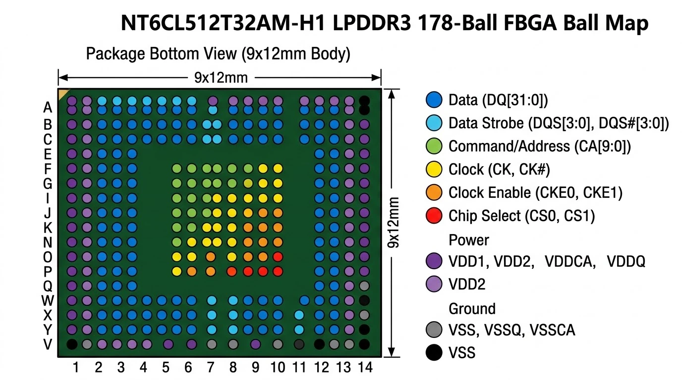
The 178-ball FBGA package body measures 9 mm × 12 mm with a 0.65 mm ball pitch in a partial-array grid layout. At 0.65 mm pitch, the PCB escape routing requires:
- Minimum trace width: 0.10 mm (4 mil) under the package
- Minimum trace-to-trace spacing: 0.10 mm (4 mil) between adjacent signal traces
- Via drill size: 0.25 mm (10 mil) drill, 0.5 mm pad for micro-vias; standard vias 0.3 mm drill for inner-layer escape
A minimum 6-layer PCB stackup is strongly recommended for LPDDR3 designs: top (signal) — ground — signal — power — ground — bottom (signal). The dedicated inner ground and power planes provide the continuous reference plane required for controlled-impedance routing at 1866 Mbps and the low-inductance power delivery needed by the DRAM's switching currents.
Signal ball groupings in the 178-ball map:
- DQ0–DQ31: 32 data pins, organized as two 16-bit bytes (lower byte DQ0–DQ15, upper byte DQ16–DQ31)
- DQS0_t/c, DQS1_t/c: 4 pins — two differential data strobe pairs (one per 16-bit byte lane)
- DM0, DM1: 2 data mask pins
- CA0–CA9: 10 command/address pins (DDR CA bus)
- CK_t, CK_c: 1 differential clock pair
- CKE0, CKE1: 2 clock enable pins (one per die in DDP)
- CS0, CS1: 2 chip select pins (one per die in DDP)
- ODT: 1 pin (may be connected to VSS inside package depending on ballout — verify from datasheet ball map)
- ZQ: 1 pin (connect to 240 Ω ±1% precision resistor to GND)
- VDD1, VDD2, VDDQ, VDDCA, VSS: Multiple power and ground balls distributed across the array
5.2 CA Training, Write Leveling, and DQ Calibration
LPDDR3 at 1866 Mbps requires a mandatory initialization and training sequence before the memory subsystem is operational. This training process is significantly different from DDR4 fly-by training:
CA Training (Command/Address Training): LPDDR3 uses a DDR CA bus — the 10-bit command/address signals are transferred at double data rate (on both rising and falling edges of CK). The timing relationship between CK and the CA bus must be calibrated to ensure setup and hold margins are met at each DRAM die. The CA training procedure involves the DRAM entering CA Training mode (via MR register write), the controller sweeping CA bus timing, and the DRAM responding with defined patterns on the DQ bus to indicate correct/incorrect CA timing.
For a DDP device like the NT6CL512T32AM-H1, each die (CS0 and CS1) must be trained independently — the two dies may have different CA propagation delays due to die-to-die variation within the DDP stack.
Write Leveling: LPDDR3 uses a point-to-point topology (unlike DDR4's fly-by) but still requires write leveling to compensate for DQS-to-CK timing skew introduced by PCB routing differences and internal die delays. The controller sweeps the write DQS phase for each byte lane and uses DRAM feedback to find the phase point where DQS crosses CK at the DRAM die.
DQ Calibration: Fine per-bit DQ timing adjustment within each byte lane, compensating for PCB trace length mismatches and package bond wire delays. The DRAM provides specific DQ output patterns (defined in JESD209-3) during calibration mode, allowing the controller to measure and correct individual DQ timing.
PCB trace length matching rules for NT6CL512T32AM-H1 at 1866 Mbps:
- Match all DQ and DM traces within a byte lane to within ±5 mil (0.127 mm)
- Match DQS_t and DQS_c within ±3 mil of each other
- Match CK_t and CK_c within ±3 mil of each other
- Match CA0–CA9 traces to within ±15 mil of each other (CA bus has more timing margin than DQ)
- Keep all LPDDR3 traces under 30 mm (1.2 inches) from AP to DRAM for reliable 1866 Mbps operation
5.3 Power Supply Decoupling and Rail Sequencing
The NT6CL512T32AM-H1's four power domains require careful decoupling and sequencing:
Decoupling capacitor recommendations:
- VDD1 (1.8 V) pins: 100 nF X5R/X7R ceramic per pin + 4.7 µF bulk at supply entry; total bulk ≥ 47 µF for both dies combined
- VDD2 / VDDQ / VDDCA (1.2 V) pins: 100 nF X5R ceramic per pin + 4.7 µF bulk at supply entry; total bulk ≥ 47 µF
- Placement: All decoupling capacitors must be placed on the same PCB layer as the DRAM (or the immediately adjacent layer accessible via short vias), within 3 mm of the corresponding power ball
Power-up sequencing (JEDEC JESD209-3 requirement):
- VDD1 must be applied before or simultaneously with VDD2/VDDQ/VDDCA — never apply VDD2/VDDQ before VDD1
- Both supply domains must reach their operating voltage range before CKE is asserted
- After both supplies are stable, apply a 200 µs minimum stabilization time before issuing the initialization command sequence (Reset, MR writes, ZQ calibration)
- The total initialization sequence (from power-stable to first READ/WRITE command available) takes approximately 2 ms, dominated by the ZQ calibration (tZQINIT = 1 µs minimum, typically longer) and training procedures
Violation of the power sequencing order — particularly applying VDD2/VDDQ before VDD1 — can cause destructive latch-up in the DRAM output drivers. Implement sequencing using the PMIC's programmable rail enable delay functions or dedicated power sequencer ICs.
6.0 How to Source Authentic NT6CL512T32AM-H1 Units
DRAM components — particularly mobile LPDDR variants — are among the most counterfeited categories in the electronic component secondary market. A counterfeit NT6CL512T32AM-H1 may be a relabeled lower-density device (8Gb SDP remarked as 16Gb DDP), a rejected lot with latent defects, or a completely non-functional component that mimics the package appearance. In a mobile platform, counterfeit DRAM manifests as system instability, random crashes, and memory test failures — problems that are extremely difficult and expensive to diagnose after product launch.
Sourcing best practices:
- Purchase from Nanya Technology authorized distributors: Arrow Electronics, Avnet, Mouser, and LCSC are established distribution partners for Nanya Technology products. These channels provide factory-traceable inventory with original packaging and date/lot codes.
- Verify the FBGA package marking: Authentic NT6CL512T32AM-H1 units are laser-marked on the FBGA mold compound with the part number, lot code, and date code. The marking should be sharp, correctly formatted, and match Nanya's standard marking conventions. Any component with ink-printed markings, inconsistent character sizing, or incorrect part number format should be rejected.
- Inspect reel label and moisture barrier bag: Authentic tape-and-reel units come in sealed moisture barrier bags (MSL 3 rated) with Nanya's reel label showing the full part number, quantity, lot code, and country of manufacture. Bags that have been re-sealed, lack humidity indicator cards, or show label inconsistencies are red flags.
- Functional density test: After board assembly, run a comprehensive memory test covering the full 2 GB address space (e.g., memtest86, Linux memtool, or the AP's built-in memory test routines). A relabeled 8Gb (1 GB) device will fail or crash when the test accesses addresses above the 1 GB boundary.
- Request Certificate of Conformance: For production volume orders, require a CoC with Nanya Technology lot traceability and original factory test documentation before accepting shipment.
For verified authentic Nanya Technology NT6CL512T32AM-H1 inventory with full traceability, competitive pricing, and expert procurement support, visit aichiplink.com.
7.0 Conclusion
The NT6CL512T32AM-H1 delivers Nanya Technology's proven LPDDR3 DDP solution for platforms requiring 2 GB of low-power mobile DRAM at 1866 Mbps from a single 178-ball FBGA component. Its combination of 16Gb DDP density, −30°C to +105°C operating range, complete JEDEC JESD209-3 LPDDR3 compliance, configurable drive strength and ODT, temperature-compensated self-refresh, and deep power management hierarchy makes it a versatile choice across the range of mobile, embedded, and industrial applications that have standardized on LPDDR3 application processors.
For new platform designs where the AP supports LPDDR4, the step up in bandwidth and power efficiency is compelling. But for the vast installed base of LPDDR3-capable SoCs — Rockchip RK3288/RK3399, MediaTek Helio P and X series, Qualcomm Snapdragon 4xx and 6xx series, and hundreds of other embedded Linux platforms — the NT6CL512T32AM-H1 remains a production-proven, commercially available, and cost-competitive solution that will continue to serve new designs through the foreseeable future.
Ready to source? Explore verified authentic Nanya Technology NT6CL512T32AM-H1 inventory with competitive pricing, volume RFQ support, and full traceability documentation at aichiplink.com — NT6CL512T32AM-H1.

Written by Jack Elliott from AIChipLink.
AIChipLink, one of the fastest-growing global independent electronic components distributors in the world, offers millions of products from thousands of manufacturers, and many of our in-stock parts is available to ship same day.
We mainly source and distribute integrated circuit (IC) products of brands such as Broadcom, Microchip, Texas Instruments, Infineon, NXP, Analog Devices, Qualcomm, Intel, etc., which are widely used in communication & network, telecom, industrial control, new energy and automotive electronics.
Empowered by AI, Linked to the Future. Get started on AIChipLink.com and submit your RFQ online today!
Frequently Asked Questions
What is the memory capacity of the NT6CL512T32AM-H1 in gigabytes?
The NT6CL512T32AM-H1 has a total capacity of 2 GB, derived from its 16Gb (gigabit) density. Since 8 bits equal 1 byte, 16Gb converts directly to 2GB, and the device is organized as 512M × 32, providing a 32-bit data interface to the memory controller.
Is the NT6CL512T32AM-H1 compatible with LPDDR3 memory controllers from Qualcomm, MediaTek, and Rockchip?
Yes, the NT6CL512T32AM-H1 is compatible with standard LPDDR3 memory controllers, as it follows the JEDEC LPDDR3 specification. This ensures interoperability with processors from Qualcomm, MediaTek, Rockchip, and others, although timing calibration and validation may still be required during system integration.
What is the difference between the H1 and H0NA speed grade suffixes for NT6CL512T32AM?
The H1 and H0NA suffixes mainly indicate variant or qualification differences rather than major performance changes. Both typically support the same 1866 Mbps speed grade, but H0NA may refer to specific production, region, or qualification requirements, so datasheet verification is recommended before substitution.
Can the NT6CL512T32AM-H1 operate at lower speeds than 1866 Mbps?
Yes, the NT6CL512T32AM-H1 supports operation at lower LPDDR3 speed grades, allowing it to run at reduced data rates with adjusted timing parameters. This flexibility helps ensure compatibility with different system designs and signal integrity conditions.
Why does the NT6CL512T32AM-H1 have a longer tRFC than an 8Gb LPDDR3 device?
The longer tRFC is due to higher memory density, as larger DRAM arrays require more time to complete refresh cycles. This results in slightly increased refresh overhead, which can have a minor impact on overall memory bandwidth in performance-critical applications.