Introduction
The Internet of Things was once a concept defined by low-power microcontrollers running bare-metal firmware — tiny, simple nodes that sensed and reported, but could not reason, route, or run a real operating system. Today's IoT is fundamentally different. Edge gateways need to run Linux, execute Python scripts, serve REST APIs, bridge Wi-Fi to cellular, transcode video, and handle TLS encryption — all on a device that must fit inside a wall outlet, a doorbell, or a factory sensor enclosure.
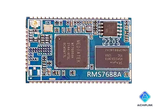
The MT7688AN from MediaTek is a System-on-Chip engineered for exactly this next-generation IoT challenge. By integrating a 580 MHz MIPS24KEc CPU, a 1T1R 802.11b/g/n Wi-Fi radio, a 5-port 100Mbps Ethernet switch, USB 2.0 host, PCIe, and a comprehensive suite of low-speed I/O peripherals — all on a single die in a 12 mm × 12 mm DR-QFN package — the MT7688AN delivers gateway-class compute and connectivity in a chipset small enough for the most space-constrained IoT designs.
According to IoT Analytics' State of IoT Report, the number of connected IoT devices globally surpassed 14 billion in 2022 and continues to grow at over 18% annually — with gateway and edge intelligence nodes representing the fastest-growing product segment. The MT7688AN powers thousands of commercial products in this category, from industrial Modbus-to-Wi-Fi bridges to consumer mesh network extenders and IP camera platforms, making it one of the most field-proven IoT SoCs in production today.
1.0 What Is the MT7688AN? An Overview
The MT7688AN is MediaTek's fully integrated appliance automation bridge SoC — the "A" variant of the MT7688 family, distinguished from the smaller MT7688KN by its expanded peripheral set, larger package, and support for DDR2 SDRAM. It is the direct successor to MediaTek/Ralink's MT7620 and part of the broader MT76xx SoC lineage inherited from Ralink Technology (acquired by MediaTek in 2011).
Decoding the part number:
- MT — MediaTek manufacturer prefix
- 7688 — Product family identifier (IoT gateway/device SoC, 802.11n integrated)
- A — Advanced variant: expanded peripheral set vs. base MT7688K; includes eMMC, SD-XC, SPI slave, 3 UARTs, PWM, and more GPIO
- N — Package type: DR-QFN (Dual Row Quad Flat No-Lead), 156 balls/pads, 12 mm × 12 mm
The companion MT7688KN is a smaller (10 mm × 10 mm, 120-pin), lower-cost variant with reduced peripheral count — DDR1 only, no eMMC, no SD-XC, fewer GPIOs — targeted at compact entry-level router and repeater applications where the MT7688AN's full peripheral suite is not required.
"MT7688AN SoC is an appliance automation bridge. It integrates a 1T1R 802.11n Wi-Fi radio, a 580MHz MIPS® 24KEc™ CPU, 1-port fast Ethernet PHY, USB2.0 host, PCIe, SD-XC, I2S/PCM and multiple low-speed IOs in a single SoC." — MediaTek Labs MT7688 Product Page
The MT7688AN achieved notable recognition when MediaTek partnered with Seeed Studio to release the LinkIt Smart 7688 development platform — an open-hardware, OpenWrt-based SBC built around the MT7688AN that brought this industrial IoT SoC into the hands of the maker and developer community worldwide.
2.0 Full Technical Specifications & SoC Architecture
2.1 MIPS24KEc CPU, Cache, and AES Hardware Engine
The MT7688AN's processor core is the MIPS24KEc — a member of the MIPS32 Release 2 architecture family from Imagination Technologies (formerly MIPS Technologies), well-established in networking and embedded Linux platforms:
- CPU Core: MIPS24KEc (MIPS32 Release 2, with DSP ASE extension)
- Clock Frequency: 575/580 MHz (datasheet specifies 575 MHz in some revisions, 580 MHz as target frequency; in practice commercial modules run at 580 MHz)
- Instruction Cache (I-Cache): 64 KB, 4-way set-associative
- Data Cache (D-Cache): 32 KB, 4-way set-associative
- FPU (Floating Point Unit): Not present — all floating-point operations are software-emulated; compute-intensive FP workloads should be avoided or pre-optimized
- DSP Extensions: MIPS DSP Application Specific Extension (ASE) — provides hardware-accelerated multiply-accumulate, saturating arithmetic, and 16-bit SIMD operations for audio DSP and signal processing
- Hardware AES Engine: AES-128 and AES-256 encryption/decryption accelerator — offloads WPA2/WPA3 Wi-Fi encryption and TLS/SSL traffic encryption from the CPU, enabling wire-speed encrypted throughput without CPU saturation
- Memory Management Unit (MMU): Full MIPS32 MMU — required for virtual memory management under Linux, enabling user-space/kernel-space separation and process isolation
- Endianness: Big-endian (default MIPS configuration)
The hardware AES engine deserves particular emphasis for IoT security applications. At 580 MHz without hardware acceleration, software AES on a MIPS24KEc achieves approximately 40–60 Mbps — adequate for light TLS traffic but insufficient for 100 Mbps encrypted tunnels (VPN, HTTPS camera streaming). With the MT7688AN's hardware AES engine, encrypted throughput approaches line rate — a critical advantage for IoT gateways handling secure cloud communication, MQTT over TLS, or encrypted video streams.
2.2 Integrated 802.11n Wi-Fi Radio (1T1R, 2.4 GHz)
The MT7688AN integrates a complete IEEE 802.11b/g/n Wi-Fi radio on the same die as the CPU:
- Standard: IEEE 802.11b/g/n (2.4 GHz band)
- Antenna Configuration: 1T1R (1 transmit, 1 receive chain — single spatial stream)
- Maximum PHY Data Rate: 150 Mbps (802.11n, 40 MHz channel, 400 ns guard interval)
- Channel Bandwidth: 20 MHz (standard), 40 MHz (optional, 802.11n HT40)
- Security: WEP-64/128, TKIP, AES-CCMP, WPA, WPA2, WAPI
- Wi-Fi Modes: AP mode, Station (STA) mode, AP+STA concurrent mode
- QoS: WMM (Wi-Fi Multimedia), WMM-PS (Power Save)
- Operating Channel Range: Channels 1–14 (region-dependent)
The 1T1R SISO (Single Input Single Output) configuration means the MT7688AN does not support MIMO — maximum 150 Mbps PHY rate under ideal conditions, with real-world TCP throughput typically in the 60–90 Mbps range depending on distance, interference, and channel conditions. For applications requiring higher Wi-Fi throughput (> 150 Mbps, 5 GHz band, or MU-MIMO), the MT7688AN's PCIe interface connects to an external 802.11ac chipset (such as MediaTek's MT7612E) to form an 802.11ac dual-band concurrent gateway — one of the device's key design use cases.
The Wi-Fi radio requires an external RF front-end comprising a matching network and antenna. MediaTek provides reference RF matching circuit designs in the MT7688AN hardware design guide. For compact module designs, a chip antenna or PCB trace antenna is most common; for router and gateway products requiring extended range, an external whip or dipole antenna connected via U.FL/IPEX connector is standard.
2.3 Peripheral Interfaces: eMMC, SD-XC, USB, I2S, PCM, PWM, UART
The MT7688AN's peripheral richness is its defining competitive advantage over lower-cost IoT MCUs. The complete peripheral inventory:
Storage Interfaces:
- SPI Flash: Dedicated SPI controller supporting 3-byte (max 128 Mbit / 16 MB) and 4-byte (max 512 Mbit / 64 MB) address modes — primary boot storage for OpenWrt firmware
- eMMC: eMMC 4.41 interface (up to 8-bit data bus) — supports high-capacity embedded flash (4 GB–32 GB) for storing large Linux root filesystems, application data, and media
- SD-XC: SDIO 3.0 / SD-XC interface — supports SD cards up to theoretical 2 TB; used for removable storage in NAS, camera, and media player applications
- 16-bit DDR Memory Bus: Supports DDR1 (MT7688KN) and DDR2 (MT7688AN) SDRAM up to 256 MB
High-Speed Interfaces:
- USB 2.0 Host (×1): High-speed 480 Mbps USB 2.0 host port — supports USB storage (mass storage class), USB-to-serial adapters, LTE/3G modems (CDC-NCM, RNDIS), USB webcams (UVC), and USB audio (UAC)
- PCIe Gen 1 (×1): Single-lane PCIe 1.0 interface — primary expansion bus for 802.11ac radio cards (MT7612E, MT7612EN) in dual-band gateway designs; also supports PCIe Ethernet cards and other PCIe peripherals
Ethernet:
- 5-Port Fast Ethernet Switch (IoT Gateway Mode): Internal 5-port 10/100 Mbps switch with MII/RGMII interface — standard for wireless router LAN port switching
- 1-Port Fast Ethernet PHY (IoT Device Mode): Single 10/100 Mbps Ethernet PHY — for device-mode applications requiring a single wired network connection
Low-Speed Interfaces (IoT Device Mode):
- I2C: Standard I2C master (100 kHz / 400 kHz) — sensor interfaces, OLED displays, EEPROMs
- SPI Master: Up to 3 chip selects — external ADCs, DACs, LCD controllers, sensor ICs
- SPI Slave: Available in IoT Device Mode — for co-processor communication (e.g., ATmega32U4 in LinkIt Smart 7688 Duo)
- I2S: 192 kHz / 24-bit I2S audio interface — high-quality audio output for Wi-Fi speakers, VoIP terminals, and smart displays
- PCM: PCM voice codec interface — VoIP handset and telephone gateway applications
- UART (×3): Three hardware UARTs in IoT Device Mode — console/debug (UART0), co-processor communication, and external modem/module interfaces
- PWM: Multiple PWM output channels — motor speed control, LED dimming, servo positioning
- GPIO: Up to 70+ GPIO pins (depending on mode and pin muxing configuration)
- JTAG: Hardware debug interface for kernel and firmware development
2.4 Power Supply Requirements and Current Consumption
The MT7688AN operates from a 3.3 V core supply with internal voltage regulators generating the lower voltages required by the CPU core and radio:
- Primary Supply Voltage (VCC): 3.3 V ± 10% (3.0 V – 3.6 V)
- DDR2 Interface Supply (VDDQ): 1.8 V (requires external LDO or DCDC from 3.3 V)
- Core Voltage (VDD_CORE): ~1.1 V (generated internally or from external LDO depending on design)
- PLL Supply (VDD_PLL): 1.8 V
Typical current consumption:
- Active (CPU running, Wi-Fi transmitting at max power): ~500–700 mA from 3.3 V (approximately 1.7–2.3 W)
- Active (CPU running, Wi-Fi idle): ~250–400 mA from 3.3 V
- Wi-Fi TX peak current: Can spike to 800+ mA for short intervals during 802.11n OFDM burst transmission — supply decoupling must handle this transient
- Idle/Low activity: ~150–200 mA
The 3.3 V supply current requirement means the MT7688AN typically requires a regulated 5 V → 3.3 V step-down converter (DCDC buck regulator, not LDO — the 2 W+ continuous power makes LDO efficiency unacceptable) as the primary power stage. Standard module implementations (HLK-7688A, Onion Omega2, etc.) integrate this converter on-board and accept 5 V or USB power input.
3.0 Software Ecosystem, Operating Modes & Applications
3.1 IoT Gateway Mode vs. IoT Device Mode
The MT7688AN's most architecturally distinctive feature is its dual operating mode — the same silicon die is configurable (via bootstrap pins at power-up) for two fundamentally different system roles:
IoT Gateway Mode: In gateway mode, the MT7688AN activates its 5-port 100Mbps Ethernet switch and optimizes for network routing and bridging functions. The PCIe port can connect to an 802.11ac external radio (forming a dual-band AC+N concurrent gateway — 5 GHz 802.11ac via PCIe card + 2.4 GHz 802.11n via internal radio). Additional gateway-mode features include: touchscreen panel support, Bluetooth Low Energy bridge capability (via USB BT dongle), Zigbee/Z-Wave/Sub-1 GHz coordination (via USB or UART adapters), and 3G/LTE modem support via USB 2.0.
IoT Device Mode: In device mode, the 5-port Ethernet switch pins are reassigned to peripheral I/O functions, enabling the expanded peripheral set that makes the MT7688AN suitable for end-node applications rather than network infrastructure: eMMC storage, SD-XC card support, SPI slave interface, three hardware UARTs, PWM outputs, and the full GPIO complement. This mode is used in IP cameras, smart speakers, industrial gateways (UART-to-Wi-Fi bridges), and development boards (LinkIt Smart 7688).
The mode selection is made at boot time via hardware bootstrap strapping resistors — it cannot be changed at runtime. Design the PCB for a fixed operating mode, and ensure the bootstrap resistors reflect the intended configuration.
3.2 OpenWrt Linux, Python, Node.js, and SDK Development
The MT7688AN runs OpenWrt Linux — the open-source embedded Linux distribution purpose-built for network devices — out of the box. This positions it firmly in a different category from microcontroller-based IoT solutions: the MT7688AN is a Linux application processor that happens to have integrated Wi-Fi, not a Wi-Fi chip with peripheral I/O.
Development environment options:
- OpenWrt: The primary OS, based on Linux kernel 3.10 (MediaTek AP SOC SDK) or later kernels (mainline OpenWrt). Full package management via opkg, mature networking stack (iptables, dnsmasq, hostapd), and extensive Wi-Fi management tools (iwconfig, iw, hostapd).
- Python 2.7/3.x: Available via OpenWrt package manager — enables rapid application prototyping, MQTT client implementation, REST API clients, and GPIO control via /sys/class/gpio
- Node.js: Supported on the LinkIt Smart 7688 platform — enables JavaScript-based IoT applications, WebSocket servers, and cloud service integration
- Native C/C++: Full GCC cross-compilation toolchain available via OpenWrt SDK for performance-critical applications (video encoding pipelines, real-time control loops)
- Arduino IDE (Duo variant): On the LinkIt Smart 7688 Duo board, the co-processor ATmega32U4 is programmable via the Arduino IDE, with the MT7688AN handling Linux-side tasks and communicating to the MCU over a dedicated serial bridge
Apple HomeKit certification: The MT7688AN has passed Apple HomeKit Adjunct Review certification for various HomeKit devices and bridges — a significant commercial advantage for smart home product manufacturers targeting the Apple ecosystem, enabling direct Siri control and Home app integration without a hub.
3.3 IP Camera, Smart Home Gateway, and Industrial IoT
The MT7688AN's feature integration makes it the reference SoC for several high-volume IoT application categories:
Wi-Fi IP Camera: The USB 2.0 host connects to a UVC-compatible H.264 image signal processor (ISP) or directly to a USB camera module. OpenWrt's mjpeg-streamer or ffmpeg package handles video encoding and RTSP/HTTP streaming. Hardware AES enables encrypted video streams without CPU bottleneck. The MT7688AN handles the complete camera-to-cloud pipeline: capture → encode → TLS encrypt → MQTT/RTSP stream → cloud storage.
Smart Home Hub/Bridge: In gateway mode with PCIe 802.11ac + internal 802.11n, the MT7688AN operates as a dual-band Wi-Fi router. USB or UART-attached Zigbee/Z-Wave/Bluetooth LE coordinators bridge smart home protocols to the IP network. OpenWrt's Home Automation support (domoticz, openHAB running via opkg) enables local processing of automation rules without cloud dependency.
Industrial UART-to-Wi-Fi Bridge (Modbus/RS-485 Gateway): Three hardware UARTs in device mode allow simultaneous connection to multiple RS-232/RS-485 industrial devices. A Python script running on OpenWrt reads Modbus RTU frames from each UART and publishes them to an MQTT broker over Wi-Fi/Ethernet — converting legacy industrial protocols to IP in a single-chip solution.
VoIP/Audio Gateway: The I2S interface (192 kHz / 24-bit capable) connects to a high-quality audio codec DAC/ADC. PCM interface supports telephony-grade voice codecs (G.711, G.722). Combined with OpenWrt's Asterisk package (SIP PBX), the MT7688AN becomes a complete Wi-Fi VoIP adapter or conference phone platform.
3.4 PCIe, USB 2.0 Host, and 5-Port FE Switch Expansion
The PCIe Gen 1 ×1 interface is the MT7688AN's primary high-bandwidth expansion bus. In gateway mode, the standard use case is connecting an 802.11ac mini-PCIe card (MT7612E or MT7612EN from MediaTek) to create a concurrent dual-band gateway. The MT7688AN's internal 2.4 GHz radio handles legacy 802.11n clients, while the PCIe-attached 5 GHz 802.11ac card handles high-bandwidth devices — a configuration found in hundreds of commercial router products.
The USB 2.0 host provides 480 Mbps bandwidth and supports the standard Linux USB class drivers available in OpenWrt:
- mass_storage: USB flash drives, hard drives (with external power), SD card readers
- cdc_ncm / rndis: 4G LTE modems (Huawei, ZTE, Sierra Wireless) for cellular WAN connectivity
- uvcvideo: USB webcams and IP camera sensors
- btusb: Bluetooth USB dongles (BT 4.x BLE adapters)
- audio: USB audio DAC/ADC for high-quality audio I/O without using the I2S pins
The 5-port 100Mbps Fast Ethernet switch (gateway mode) provides enough LAN bandwidth for 4 wired clients at 100 Mbps full duplex simultaneously, with the 5th port connected internally to the MT7688AN's CPU via a GMAC interface. The switch supports VLAN tagging (802.1Q) for traffic segmentation between WAN and LAN ports.
This video covers MT7688AN hardware bring-up, OpenWrt first boot, Python and Node.js environment setup, GPIO control, and Wi-Fi configuration for IoT gateway and device mode applications.
4.0 MT7688AN vs. Competing IoT SoCs
4.1 MT7688AN vs. MT7688KN, MT7628AN, and Atheros AR9331
| Feature | MT7688AN | MT7688KN | MT7628AN | Atheros AR9331 |
|---|---|---|---|---|
| CPU Core | MIPS24KEc | MIPS24KEc | MIPS24KEc | MIPS24K |
| CPU Frequency | 580 MHz | 580 MHz | 580 MHz | 400 MHz |
| Wi-Fi | 802.11b/g/n 1T1R | 802.11b/g/n 1T1R | 802.11b/g/n 2T2R | 802.11b/g/n 1T1R |
| Max Wi-Fi Rate | 150 Mbps | 150 Mbps | 300 Mbps | 150 Mbps |
| DDR Support | DDR1 + DDR2 | DDR1 only | DDR1 + DDR2 | DDR1 + DDR2 |
| Max RAM | 256 MB | 128 MB (DDR1) | 256 MB | 128 MB |
| eMMC | Yes | No | No | No |
| SD-XC | Yes | No | Yes | No |
| USB 2.0 Host | Yes | Yes | Yes | Yes |
| PCIe | Yes | Yes | Yes | No |
| UART Count | 3 (device mode) | 2 | 3 | 2 |
| I2S Audio | Yes (192kHz/24b) | No | No | No |
| PCM | Yes | No | No | No |
| PWM | Yes | No | Yes | No |
| Package | DR-QFN 156 (12×12mm) | DR-QFN 120 (10×10mm) | QFN (12×12mm) | QFN (9×9mm) |
| OpenWrt Support | Mainline | Mainline | Mainline | Mainline |
| Apple HomeKit | Certified | Not listed | Not listed | No |
Key selection guidance:
- Need maximum peripheral richness, DDR2, eMMC, I2S audio, 3 UARTs → MT7688AN — this device; the most fully-featured member of the MT7688 family, used in design-in products requiring Linux + rich I/O
- Need lowest-cost single-die 802.11n router chipset → MT7688KN — reduced peripherals, DDR1 only, smaller 10×10 mm package; used in compact routers and repeaters where eMMC/SD/I2S are not required
- Need 2T2R dual-stream Wi-Fi (300 Mbps) for higher throughput → MT7628AN — pin-compatible with MT7688 series, 2T2R antenna, same CPU/frequency; the preferred choice when Wi-Fi throughput matters more than audio/eMMC peripherals
- Working with legacy designs based on Atheros/Qualcomm → AR9331 — older 400 MHz platform, no PCIe, no eMMC, no I2S; extensive community support (OpenWrt ath79 target) but slower CPU and fewer peripherals than MT7688AN
4.2 Module Ecosystem, Pricing & Availability
The MT7688AN is available both as a bare SoC die (for custom PCB designs) and as a complete SoM (System-on-Module) from multiple vendors — the module route dramatically reduces hardware development time and risk by providing pre-validated, FCC/CE-certified Wi-Fi RF designs:
Bare SoC:
- Direct procurement from MediaTek's authorized distributors (Arrow, Avnet, Future Electronics)
- Typical bare SoC pricing: ~$4–$8 USD per unit (volume-dependent)
- Requires full board-level design including DDR2, SPI flash, power management, RF matching, and antenna
Ready-to-use modules based on MT7688AN:
- HLK-7688A (Hi-Link): 128 MB DDR2 + 32 MB SPI flash, FCC/CE certified, ~$8–$12 USD
- Onion Omega2 / Omega2S: 64 MB DDR2 + 16 MB flash (Omega2), or 128 MB DDR2 + 32 MB flash (Omega2+), ~$5–$13 USD; popular in maker community
- LinkIt Smart 7688 (Seeed Studio / MediaTek Labs): 128 MB DDR2 + 32 MB flash, development-oriented with full pin headers, ~$12–$15 USD
- DWM-JS7688 and similar OEM modules: 64/128/256 MB DDR2 configurations, stamp-hole or pin-header mounting
Apple HomeKit: The MT7688AN has passed Apple HomeKit Adjunct Review certification — product manufacturers using this SoC in HomeKit accessories can reference MediaTek's certification documentation to accelerate their own MFi certification process.
For competitive pricing on bare MT7688AN SoC units, authentic MediaTek inventory with full traceability, and volume procurement support, visit aichiplink.com — MT7688AN listing.
5.0 Hardware Design and PCB Guidelines
5.1 156-Pin DR-QFN Package and PCB Footprint
The MT7688AN is housed in a DR-QFN (Dual Row Quad Flat No-Lead) package with 156 pads arranged in two concentric rows around the perimeter of a 12 mm × 12 mm body at a 0.5 mm pad pitch. A large central exposed pad (EP) provides both the primary thermal path and a ground connection for the die substrate.
PCB design requirements for the DR-QFN-156:
- Pad dimensions: 0.3 mm × 0.6 mm per pad (outer row), as specified in MediaTek's package drawing; verify against your PCB manufacturer's capabilities — 0.5 mm pitch QFN requires 4-mil/4-mil minimum trace/space rules
- Exposed pad (EP): Must be soldered to a solid ground plane beneath the package. Add a 6×6 grid of 0.3 mm thermal vias (filled or tented) under the EP, connecting to the inner PCB ground plane for both thermal relief and RF ground integrity
- Stencil design: Use a 0.12–0.15 mm stencil aperture reduction on the EP to prevent solder bridging to the outer pads during reflow
- Reflow profile: Standard lead-free SAC305 profile — preheat 150–180°C, soak 180–220°C, peak ≤ 260°C, time above liquidus ≤ 30 seconds
- X-ray inspection: Mandatory for production — the EP solder joint is not visually inspectable; X-ray confirms full EP wetting and absence of voids
The dual-row pad arrangement requires careful escape routing under the package. Inner-row pads escape to layer 2 via micro-vias (0.2 mm drill), while outer-row pads can be fanned out on the top layer with 0.15 mm traces before routing to internal layers. A minimum 6-layer PCB stackup (signal–ground–signal–signal–power–signal) is recommended for designs using DDR2 memory alongside the RF signals.
5.2 DDR2 Memory Interface Layout and Signal Integrity
The MT7688AN supports a 16-bit DDR2 SDRAM interface capable of addressing up to 256 MB of external DRAM. The DDR2 interface operates at up to DDR2-400/DDR2-800 speeds depending on memory configuration. Key layout rules:
- Topology: Point-to-point (one DRAM device per channel) — no fly-by topology required for DDR2 at these data rates; shorter stub connections are preferred
- Trace length matching: Match all 16 DQ data lines within ±5 mil (0.127 mm) of each other; match DQS/DQS_n differential pair traces to within ±3 mil; match CLK/CLK_n differential pair to within ±3 mil
- Reference planes: Route all DDR2 signals over continuous ground or power planes — no splits or gaps in the reference plane beneath DDR2 traces
- Decoupling capacitors: Place 100 nF + 10 nF ceramic decoupling capacitors at each VDD, VDDQ, and VTT power pin of the DRAM device, within 3 mm of the pin
- VDDQ (1.8 V): Requires a dedicated, low-noise 1.8 V LDO or DCDC converter. Use a Pi filter (inductor + input/output capacitors) at the VDDQ supply entry point to prevent SoC switching noise from coupling into the memory interface
- ODT termination: DDR2 uses on-die termination (ODT) within the DRAM die itself — no external termination resistors are required on the data bus, simplifying the layout compared to older DDR1 designs
- Max trace length: Keep DDR2 trace lengths below 5 cm (2 inches) for reliable operation at DDR2-400/800 speeds on standard FR4 material
5.3 RF Layout, Antenna Design, and Power Decoupling
The MT7688AN integrates the entire 802.11n RF transceiver, requiring only an external matching network, RF switch (if needed), and antenna:
RF matching network: MediaTek provides a reference matching circuit in the hardware design guide. A typical implementation uses a low-pass LC matching network between the RF_OUT pin and the antenna connector/trace. Component values are optimized for 2.4 GHz (2400–2484 MHz) operation and must be precisely placed and routed.
Antenna options:
- PCB trace antenna: Inverted-F antenna (IFA) printed directly on the PCB — zero component cost, requires careful PCB area allocation (typically 30–40 mm long), sensitive to nearby copper pours and keepout violations
- Chip antenna: 0402 or 0603 ceramic chip antenna (e.g., Molex, Taoglas series) — more compact than trace antenna, less sensitive to PCB keepout, slightly higher insertion loss
- External antenna via U.FL/IPEX connector: Best for applications requiring directional gain or remote antenna placement (enclosure-mounted antennas, external dipoles)
RF keepout rules:
- No copper pours or signal traces within 15 mm of the antenna element — violating this rule will detune the antenna and severely reduce Wi-Fi range
- Ground plane cutout beneath the antenna: For PCB trace antennas, remove the ground plane directly below the antenna element on all PCB layers
- RF trace routing: Route the RF matching network traces as 50 Ω coplanar waveguide (CPW) — use a coplanar ground on the same layer alongside the trace, with via stitching to the ground plane
Power supply decoupling for the SoC:
- Place 10 µF + 100 nF ceramic capacitors at each VCC (3.3 V) supply pin of the MT7688AN
- Place a 47 µF bulk capacitor near the 3.3 V main supply entry point on the PCB
- The Wi-Fi TX current surge (potentially 200–300 mA transient) must be sourced from local decoupling, not from the power supply trace inductance — insufficient decoupling causes supply droops that reset the SoC or corrupt the Wi-Fi transmit waveform
6.0 How to Source Authentic MT7688AN Units
The MT7688AN's widespread use in consumer and industrial IoT products has made it a target for counterfeit and remarked parts in the secondary market. A counterfeit chip may execute basic MIPS code but fail to initialize the DDR2 interface, fail to achieve rated Wi-Fi TX power (causing range degradation), or lack the hardware AES engine (causing CPU overload during encrypted traffic). In production IoT devices, these failures often manifest as intermittent connectivity drops or cryptographic throughput limitations rather than obvious boot failures.
Sourcing guidelines:
- Purchase from MediaTek's authorized distributors: Arrow, Avnet, Future Electronics, and Mouser are authorized MediaTek distribution partners. These channels provide factory-sealed, traceable inventory with original MediaTek packaging.
- Verify package marking: Authentic MT7688AN dies are marked with the MediaTek logo, part number, lot code, and date code. The marking is laser-etched on the QFN mold compound. Compare the marking font and character spacing against MediaTek reference images.
- For rapid development, use certified modules: Modules like the HLK-7688A (Hi-Link) and Onion Omega2 integrate authenticated MT7688AN silicon with pre-certified RF designs, saving both sourcing risk and RF compliance testing time and cost.
- Functional validation: At board bring-up, verify CPU clock frequency (check /proc/cpuinfo for "BogoMIPS" around 1160 — corresponding to 580 MHz × 2), confirm DDR2 memory size via /proc/meminfo, run a Wi-Fi throughput test (iperf3 to a nearby client — should achieve > 50 Mbps TCP), and test hardware AES acceleration (OpenSSL speed test comparing aes-128-cbc with and without engine — hardware AES should be 3–5× faster).
- Request CoC for production volumes: For volume bare-SoC procurement, demand a Certificate of Conformance with MediaTek lot traceability before accepting delivery.
For verified authentic MediaTek MT7688AN inventory, competitive pricing, and volume RFQ support, visit aichiplink.com — MT7688AN.
7.0 Conclusion
The MT7688AN has earned its status as one of the most widely deployed Linux-capable IoT SoCs in production hardware. Its combination of 580 MHz MIPS24KEc CPU, integrated 802.11b/g/n 1T1R Wi-Fi, 5-port Ethernet switch (gateway mode), USB 2.0 host, PCIe expansion, eMMC and SD-XC storage, 192 kHz/24-bit I2S audio, hardware AES encryption, and 3 hardware UARTs (device mode) — all on a single die in a 12 mm × 12 mm DR-QFN package running full OpenWrt Linux — represents a level of integration that no discrete component design can match at comparable cost and footprint.
Its dual operating mode philosophy — configurable as either a Wi-Fi router/gateway or a feature-rich IoT device processor — gives hardware designers a single SKU that addresses two fundamentally different product architectures, reducing component inventory and simplifying certification processes. The mature OpenWrt ecosystem, Python/Node.js support, active community, and Apple HomeKit certification pathway further lower the software development barrier for commercial product development.
For engineers building industrial IoT gateways, Wi-Fi IP cameras, smart home bridges, VoIP adapters, or connected audio devices, the MT7688AN remains a battle-tested, production-proven platform with an active ecosystem and broad supply chain availability.
Ready to design in the MT7688AN? Source verified authentic MediaTek inventory — bare SoC or certified module options — with competitive pricing and volume procurement support at aichiplink.com — MT7688AN.

Written by Jack Elliott from AIChipLink.
AIChipLink, one of the fastest-growing global independent electronic components distributors in the world, offers millions of products from thousands of manufacturers, and many of our in-stock parts is available to ship same day.
We mainly source and distribute integrated circuit (IC) products of brands such as Broadcom, Microchip, Texas Instruments, Infineon, NXP, Analog Devices, Qualcomm, Intel, etc., which are widely used in communication & network, telecom, industrial control, new energy and automotive electronics.
Empowered by AI, Linked to the Future. Get started on AIChipLink.com and submit your RFQ online today!
Frequently Asked Questions
What is the difference between MT7688AN and MT7688KN?
MT7688AN and MT7688KN share the same CPU and Wi-Fi capabilities, but the MT7688AN offers more interfaces and supports DDR2 memory up to 256MB, while the MT7688KN uses a smaller package and supports fewer peripherals with up to 128MB DDR1 memory.
Can MT7688AN run Linux?
Yes, the MT7688AN can run Linux-based systems, with OpenWrt being the most commonly used distribution because it provides optimized drivers and strong community support.
What is the maximum RAM supported by MT7688AN?
The chip supports up to 256MB of DDR2 SDRAM through a 16-bit memory interface, though many devices commonly use 128MB.
How is the operating mode selected in MT7688AN?
The operating mode is determined by hardware strap pins sampled during power-up, which define the device configuration before the system boots.
Is MT7688AN suitable for battery-powered IoT devices?
The MT7688AN is designed for Linux-based networking devices and typically consumes more power than microcontroller solutions, making it less suitable for long-term battery-powered IoT applications.