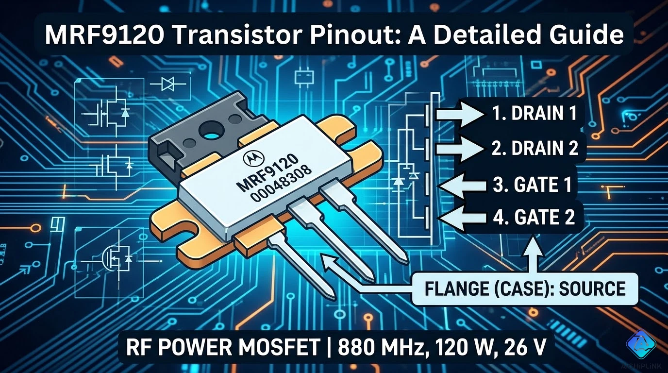
Introduction
The MRF9120 is a 20-watt RF power transistor manufactured by NXP (formerly Motorola/Freescale), widely used in amateur radio transmitters, two-way radio amplifiers, and RF power amplifier circuits operating in the 150-175 MHz frequency range. Understanding the MRF9120 pinout is critical for proper circuit connection—incorrect wiring can damage the transistor or result in poor performance. This step-by-step guide explains the MRF9120 pin configuration, identification methods, and practical connection examples for reliable RF amplifier construction.
MRF9120 Overview
Key Specifications
| Parameter | Value |
|---|---|
| Output Power | 20W typical @ 150 MHz |
| Frequency Range | 136-174 MHz |
| Supply Voltage | 12.5V (typical) |
| Gain | 14 dB (typical) |
| Package | NI-360 (plastic, 4-pin) |
| Pin Count | 4 pins |
| Technology | MOSFET (lateral N-channel) |
Common Applications
- VHF amateur radio transmitters (2-meter band: 144-148 MHz)
- Commercial two-way radio power amplifiers (VHF business band)
- Marine VHF radios (156-162 MHz)
- FM broadcast transmitters (low power)
- RF test equipment
Why Pinout Matters
Critical Reasons:
- Prevent damage: Reversed connections destroy transistor
- Ensure performance: Correct impedance matching requires proper pin identification
- Safety: RF power (20W) with wrong connections creates hazards
- Troubleshooting: Knowing pinout speeds up circuit debugging
Pin Configuration & Identification
MRF9120 Pinout (4-Pin Package)
Package View (Top View, Leads Down):
         MRF9120
    ┌─────────────┐
    │             │
    │   MOSFET    │  (Metal tab at top = DRAIN)
    │   Die       │
    │             │
    └─────────────┘
      │  │  │  │
      1  2  3  4

Pin 1: GATE (Input)
Pin 2: SOURCE (Ground)
Pin 3: SOURCE (Ground)
Pin 4: DRAIN (Output) - connects to metal tab
Alternative Pin Naming:
Pin 1: Gate (G)
Pin 2: Source (S)
Pin 3: Source (S)
Pin 4: Drain (D)
Physical Pin Identification
Method 1: Visual Inspection (Most Reliable)
Step 1: Hold transistor with metal tab facing UP and pins facing DOWN
Step 2: Number pins left to right: 1, 2, 3, 4
    [Metal Tab = DRAIN]
    ┌───────────────┐
    │   MRF9120     │
    │   (Markings)  │
    └───────────────┘
      1   2   3   4
     Gate S  S  Drain
Step 3: Verify with datasheet markings:
- Pin 1 (leftmost): Small dot or notch near Gate
- Metal tab: Always DRAIN connection
Method 2: Datasheet Verification
Download official NXP datasheet:
- Search: "MRF9120 datasheet PDF"
- Find: Pin configuration diagram (usually page 1-2)
- Confirm: Pin numbering matches physical package
Method 3: Multimeter Testing (Use with Caution)
MOSFET Body Diode Test:
- Set multimeter to diode test mode
- Measure Gate to Source: Open circuit (no reading)
- Measure Drain to Source: Body diode (~0.5-0.7V one direction)
- WARNING: Static-sensitive—use ESD protection!
Step-by-Step Connection Guide
Step 1: Identify Pins
Action:
- Orient transistor: Metal tab UP, pins DOWN
- Count from LEFT: Pin 1 (Gate), 2 (Source), 3 (Source), 4 (Drain)
- Mark pins with marker if needed
Visual Confirmation:
Look for:
- Pin 1: Closest to left edge (Gate)
- Pins 2 & 3: Middle pins (both Source/Ground)
- Pin 4: Closest to right edge (Drain/Output)
- Metal tab: Top of package (Drain connection)
Step 2: Prepare PCB or Breadboard
For PCB:
- Verify PCB footprint matches NI-360 package
- Check pin spacing: Standard 0.1" (2.54mm) between pins
- Ensure thermal pad for metal tab connection
For Breadboard (Prototyping):
- Not recommended for final design (RF performance issues)
- If using: Keep leads short (<5mm), add ground plane
Step 3: Connect Gate (Pin 1 - INPUT)
Gate Connection:
RF Input Signal → Input Matching Network → Pin 1 (Gate)

Typical input matching:
- Series capacitor (e.g., 100pF) for DC blocking
- Parallel inductors for impedance transformation
- Resistor (10Ω) for stability (optional)
Example Circuit:
RF_IN ─┬─[100pF]─┬──[Matching]── Pin 1 (Gate)
       │         │
      [10Ω]     GND
    (stability)
Step 4: Connect Source (Pins 2 & 3 - GROUND)
Source Pins (Both Pins 2 and 3):
Critical: Connect BOTH pins to ground!
Pin 2 (Source) ───┬─── GND Plane
Pin 3 (Source) ───┘

Why both?
- Lower ground inductance
- Better RF performance
- Higher current handling
PCB Layout Tips:
- Wide, short traces to ground plane
- Via stitching around source pins
- Minimum trace length (<2mm)
Step 5: Connect Drain (Pin 4 - OUTPUT)
Drain Connection:
Pin 4 (Drain) → Output Matching → RF Load (50Ω antenna)
      ↑
   DC Supply (12.5V via RFC)
Typical Output Network:
+12.5V ─[RFC]─┬── Pin 4 (Drain)
              │
         [Matching Network] → RF_OUT (50Ω)
              │
            [Bypass Caps]
RFC (Radio Frequency Choke):
- Inductance: 1-10µH
- Prevents RF from entering power supply
- Allows DC voltage to reach drain
Step 6: Connect Metal Tab (DRAIN Ground Return)
Metal Tab Connection:
Purpose: Heat dissipation + drain electrical connection
Connection Method:
- Solder tab directly to PCB ground plane
- Use thermal paste if adding heatsink
- Ensure good electrical AND thermal contact
    [Heatsink (optional)]
           │
    [Metal Tab = Drain]
           │
    [PCB Ground Plane]
Thermal Management:
- Copper PCB area: Minimum 2 square inches under tab
- Heatsink: Required for continuous operation at 20W
- Thermal compound: Arctic Silver or equivalent
Practical Circuit Example
Basic 20W VHF Amplifier (150 MHz)
Complete Pin Connections:
                    MRF9120
                 ┌───────────┐
RF_IN → [Input  │ 1  2  3  4│ → RF_OUT
         Match]  └───────────┘   [Output
                   G  S  S  D     Match]
                   │  │  │  │
                   │  │  │  └─[RFC]─+12.5V
                   │  ├──┴─── GND
                   │
                [Bias Network]
                   │
                  GND

Input Matching: 50Ω → ~5Ω (Gate impedance)
Output Matching: ~5Ω (Drain impedance) → 50Ω
Component Values (Example for 150 MHz):
Input Network:
- C1 (DC block): 100pF
- L1 (matching): 47nH
- C2 (bypass): 1000pF to GND
Output Network:
- L2 (matching): 68nH
- C3 (tuning): 47pF
- C4 (output coupling): 100pF
Bias:
- R1 (gate bias): 1kΩ
- R2 (voltage divider): 220Ω
- C5 (RF bypass): 0.1µF
Power Supply Connections
Voltage Rail:
+12.5V Supply:
- Connect via RFC (1-10µH) to Drain (Pin 4/Metal Tab)
- Bypass with 100nF ceramic + 10µF electrolytic at supply point
- Separate RF ground from power supply ground if possible
Ground Connections:
Critical Ground Points:
1. Pins 2 & 3 (Source) → Star ground point
2. Metal tab → Ground plane (thermal + electrical)
3. Bypass capacitors → Ground near pins
4. Input/output matching networks → Ground
Common Mistakes to Avoid
Mistake 1: Reversed Gate and Drain
❌ Wrong: Connecting RF input to Pin 4 (Drain)
✅ Correct: RF input connects to Pin 1 (Gate only)
Result if wrong: No RF output, possible transistor damage
Mistake 2: Single Source Ground
❌ Wrong: Connecting only Pin 2 or Pin 3 to ground
✅ Correct: Connect BOTH Pins 2 AND 3 to ground
Why: Higher inductance, reduced performance, overheating risk
Mistake 3: Ignoring Metal Tab Connection
❌ Wrong: Leaving metal tab unconnected
✅ Correct: Solder tab to PCB ground plane + add heatsink
Result if wrong: Poor thermal dissipation, transistor overheating, failure
Mistake 4: No Input/Output Matching
❌ Wrong: Direct 50Ω connection to Gate/Drain
✅ Correct: Use impedance matching networks
Why: Gate/Drain impedance ≠ 50Ω; mismatch causes poor power transfer
Testing & Verification
Step 1: Visual Inspection
Checklist:
- All 4 pins soldered
- No solder bridges between pins
- Metal tab soldered to ground plane
- Input connected to Pin 1 (Gate)
- Drain (Pin 4) connected to supply via RFC
Step 2: DC Voltage Check (Power OFF)
Multimeter Checks:
- Gate to Source: Open circuit (high resistance)
- Drain to Source: Body diode (~0.5-0.7V one direction)
Step 3: Power-On Test (No RF Signal)
Expected DC Readings:
- Drain voltage: ~12.5V (with small quiescent current <50mA)
- Gate voltage: Bias voltage (typically 2-4V depending on circuit)
Step 4: RF Performance Test
With RF Signal Generator:
- Input: 1W @ 150 MHz
- Expected output: 14-20W (depending on matching)
- Monitor: Drain current (should be 3-4A at full power)
Conclusion
Understanding the MRF9120 transistor pinout—Pin 1 (Gate/input), Pins 2-3 (Source/ground), Pin 4 (Drain/output), and metal tab (drain/thermal)—is essential for successful RF power amplifier construction. Correct pin identification, proper grounding of both Source pins, appropriate input/output matching networks, and adequate thermal management through heatsinking enable reliable 20W RF output at 150 MHz for amateur radio, two-way radio, and VHF communication applications.
Key Takeaways:
✅ Pin 1 = Gate (RF input) - leftmost pin
✅ Pins 2 & 3 = Source (ground) - BOTH must connect to ground
✅ Pin 4 = Drain (RF output + DC supply) - rightmost pin
✅ Metal tab = Drain connection - solder to ground plane
✅ Impedance matching required - Gate/Drain ≠ 50Ω
✅ Heatsink mandatory - 20W dissipation requires cooling
✅ Supply voltage: 12.5V DC via RFC to drain
Building RF amplifiers? Visit AiChipLink.com for RF transistor sourcing, pinout verification, and amplifier design consultation.

Written by Jack Elliott from AIChipLink.
AIChipLink, one of the fastest-growing global independent electronic components distributors in the world, offers millions of products from thousands of manufacturers, and many of our in-stock parts is available to ship same day.
We mainly source and distribute integrated circuit (IC) products of brands such as Broadcom, Microchip, Texas Instruments, Infineon, NXP, Analog Devices, Qualcomm, Intel, etc., which are widely used in communication & network, telecom, industrial control, new energy and automotive electronics.
Empowered by AI, Linked to the Future. Get started on AIChipLink.com and submit your RFQ online today!
Frequently Asked Questions
What is the MRF9120 pinout?
The MRF9120 uses a 4-pin NI-360 package with Gate, Source, Source, and Drain connections. When viewed with the metal tab facing up and pins downward, the pins from left to right are Gate (Pin 1), Source (Pin 2), Source (Pin 3), and Drain (Pin 4), with the metal tab also connected to the Drain for output and heat dissipation.
How do I identify Pin 1 on the MRF9120?
Pin 1 is the leftmost pin when the transistor is oriented with the metal tab facing up and pins downward. It is typically marked by a dot or notch on the package, and correct identification is critical since miswiring the Gate and Drain can permanently damage the device.
Can I connect only one Source pin to ground?
No, both Source pins must be connected to ground for proper operation. Using both pins reduces inductance, improves thermal performance, and ensures stable RF operation, while using only one can lead to reduced gain, instability, and overheating.
What voltage should I apply to the MRF9120 drain?
The MRF9120 typically operates with a 12.5V DC supply applied to the Drain. This voltage is usually fed through an RF choke to isolate the signal, and a stable, low-noise power supply is essential to ensure proper performance and avoid damage.
Do I need a heatsink for the MRF9120?
Yes, a heatsink is required for continuous operation to manage heat dissipation. Without proper cooling, the device can overheat due to power loss, so using a heatsink or sufficient PCB thermal design is necessary to maintain safe operating temperatures.