You can connect the High-Precision AD5541 DAC to your FPGA using the SPI lines for wiring. Make sure the frequency matches your system requirements. The FPGA sends digital data to the High-Precision AD5541 DAC through SPI communication, allowing you to generate a high-precision analog signal. Set the voltage range for the High-Precision AD5541 DAC and control noise to maintain a steady frequency output. This setup works best with proper frequency management. Using field programmable gate arrays enhances performance. For accurate results, refer to application notes and design guides specific to the High-Precision AD5541.
Tip: Good frequency planning helps your FPGA and High-Precision AD5541 DAC work well together.
Key Takeaways
-
Connect the AD5541 DAC to your FPGA with short wires. Use short wires for SCLK, DIN, CS, and LDAC pins. This helps keep signals clean and stable.
-
Use SPI mode 0 with CPOL set to 0 and CPHA set to 0. Send 16-bit data while the chip select line is low. This makes communication accurate.
-
Calibrate your system by sending known values. Measure the output voltage each time. Adjust your FPGA code to get precise analog signals.
-
Design your PCB with short signal paths. Make sure you have good grounding. Put decoupling capacitors near the DAC. This lowers noise and makes things more stable.
-
Test and take care of your setup often. Use oscilloscopes or logic analyzers to check it. This keeps your system accurate and working well for a long time.
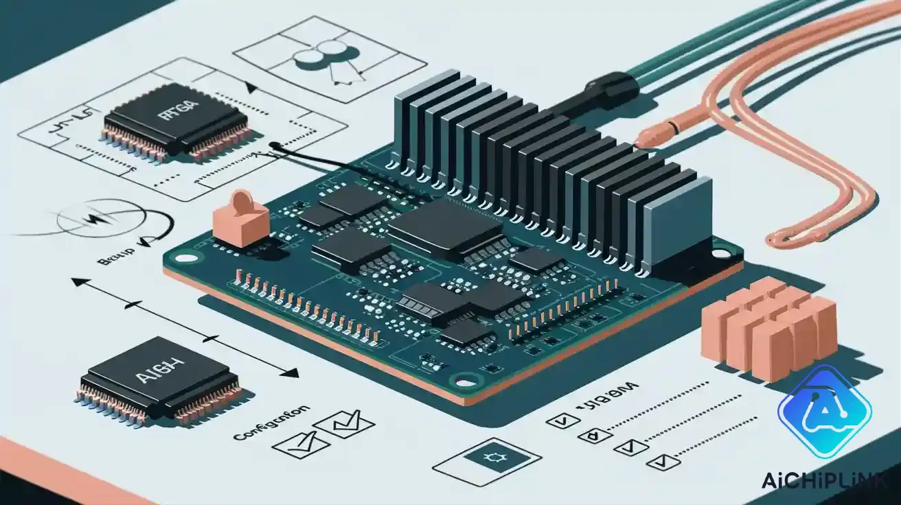
High-Precision AD5541 FPGA Integration
You can get very accurate analog output by connecting the high-precision AD5541 DAC to your FPGA. This setup lets you control voltage well, which is important for things that need steady and reliable analog signals. The high-precision AD5541 DAC uses a simple SPI interface, so it is easy to connect to most FPGA boards. When you use field programmable gate arrays, you can send digital signals to the DAC and turn them into smooth, high-precision analog output. The Analog Devices CN0169 application note shows you how to connect everything step by step. It explains how to send 16-bit data from the FPGA to the DAC and how to keep your signals clean for the best results. Many engineers use Pmod interface boards, like the Digilent Pmod DA3, to make wiring easier and help the signals stay strong. These boards help you set up your system fast and lower the chance of making wiring mistakes.
Hardware Requirements
To connect the high-precision AD5541 DAC to your FPGA, you need some hardware:
-
FPGA board to make clock and control signals for the DAC
-
High-precision AD5541 DAC chip, often on a Pmod board like the Digilent Pmod DA3
-
Good power supply (2.7 V to 5.5 V) for both the FPGA and DAC
-
Short, direct wires to cut down noise and signal loss
-
Decoupling capacitors close to the DAC power pins to block noise
-
Optional: Oscilloscope or logic analyzer to test and check timing and analog output
You also need to connect these main signal lines between the FPGA and the DAC:
-
SCLK (Serial Clock): Sends the clock from the FPGA to the DAC
-
~CS (Chip Select): Lets the DAC get data when pulled low
-
DIN (Data Input): Sends the 16-bit data from the FPGA to the DAC
-
~LDAC (Load DAC): Updates the DAC output when pulled low
Note: Keep your power rails clean and steady. Put decoupling capacitors close to the DAC. Use short wires and keep them away from high-current wires to keep your analog output accurate.
Connection Diagram
The best way to connect the high-precision AD5541 DAC and FPGA is to use the SPI interface. You connect the SCLK, DIN, CS, and ~LDAC lines from the FPGA to the matching pins on the DAC. The chip select (CS) line should stay low during the whole 16-bit data transfer. The FPGA sends data on the DIN line, and the DAC reads it when the SCLK goes up. If you keep the LDAC line low, the DAC updates its output right after each data transfer. Always follow the timing diagram in the AD5541 datasheet to make sure the data is sent right and the analog output updates as it should.
Using a Pmod interface board, like the Digilent Pmod DA3, makes this easier. The Pmod board holds the DAC and has pins that match the FPGA signals. This keeps wires short and direct, which helps keep the analog output accurate. The Pmod board also has a voltage reference and meets the timing needs of the DAC, so your setup is smoother and more reliable.
You should always test your system with a logic analyzer or oscilloscope. This helps you check the timing and make sure your analog output is correct. The CN0169 application note from Analog Devices gives more details, including example Verilog code for SPI communication and tips for calibration and debugging.
Wiring and Pin Mapping
FPGA to AD5541 Connections
You need to connect your fpga to the ad5541 dac chip using the correct pins. The dac uses a SPI interface. You will use four main lines for this connection. The SCLK pin on the fpga sends clock pulses to the dac. The DIN pin carries the serial data from the fpga to the dac. The CS pin selects the dac device when you want to send data. The LDAC pin tells the dac when to update its output. When you pull LDAC low, the dac updates the readout right after each data transfer. This setup helps you control the timing and frequency of your analog signal.
You should match the SPI port names on your fpga to the dac pins. The SCLK line connects to the SCLK pin, DIN to DIN, and CS to CS. The LDAC pin can connect to a general-purpose output on your fpga. This lets you control when the dac updates its readout. You will send 16-bit data words from the fpga to the dac. Each word sets the analog output. The frequency of the SCLK signal controls how fast you send data. You can use this setup for lock-in readout, signal acquisition, and other high-precision tasks. Always check your wiring to keep signal integrity high and avoid errors in your data acquisition.
Power and Ground
You must give the ad5541 dac chip a clean power supply. Connect the VDD pin to a stable voltage source. Most fpga boards use 3.3V or 5V. Make sure the ground (GND) of the fpga and the dac are tied together. This keeps the signal levels correct and helps with signal integrity. Place decoupling capacitors close to the dac power pins. These capacitors block noise and keep the voltage steady during data acquisition and readout.
Short wires help reduce noise and keep your signal clean. Keep the analog signal lines away from high-frequency digital lines on your board. This helps prevent interference during lock-in acquisition and readout. Good power and ground connections make your frequency output stable and reliable. You will see better results in your lock-in signal acquisition and readout if you follow these steps.
Tip: Always double-check your power and ground connections before you start your data acquisition or lock-in readout. A small wiring mistake can cause big problems in your signal.
SPI Configuration
SPI Protocol
You use SPI communication to send digital data from your fpga to the dac. SPI stands for Serial Peripheral Interface. This protocol uses four main lines: SCLK (clock), DIN (data in), CS (chip select), and LDAC (load dac). You control the timing and order of each signal to make sure the dac gets the right data.
When you want to send data, you pull the chip select (CS) line low. This tells the dac to listen for new data. You send 16 bits of data, one bit at a time, on the DIN line. The fpga creates clock pulses on the SCLK line. The dac reads each bit on the rising edge of the clock. You must keep the CS line low for the whole data transfer. After you send all 16 bits, you bring CS high. This latches the data into the dac and updates the analog output.
The LDAC line controls when the dac updates its output. If you keep LDAC low, the dac updates right after each data transfer. If you want to control the update timing, you can pulse LDAC low after sending data. This gives you more control over when the analog signal changes.
Tip: Always match the SPI mode to the dac's requirements. For the AD5541, use CPOL=0 and CPHA=0. This means the clock starts low, and the dac reads data on the rising edge.
Timing and Data Transfer
Signal timing is very important in spi communication. The fpga must follow the timing rules in the dac datasheet. You must keep the CS line low during the whole 16-bit transfer. The dac expects each bit to arrive on the DIN line just before the rising edge of SCLK. The data must stay stable at each clock edge. After you finish sending data, you must wait at least 15-20 nanoseconds before starting a new transfer. This pause helps the dac process the last data and get ready for the next one.
The fpga sends the most significant bit first. You control the frequency of the SCLK signal to match the dac's maximum speed. If you send data too fast, the dac may not read it correctly. If you send it too slow, your analog signal may lag. You must find the right balance for your application.
Here is a simple VHDL code example for spi communication with the AD5541 dac. This code uses a state machine to manage the transaction. It sets the clock frequency, waits for the right signal timing, and sends 16 bits of data from the fpga to the dac.
-- Simple VHDL SPI Controller for AD5541 DAC
process(clk)
    variable bit_cnt : integer range 0 to 15 := 0;
    variable data_reg : std_logic_vector(15 downto 0);
begin
    if rising_edge(clk) then
        if start_transfer = '1' then
            cs <= '0'; -- Start transfer
            data_reg := data_in; -- Load data
            bit_cnt := 15;
        elsif cs = '0' then
            sclk <= not sclk; -- Toggle clock
            if sclk = '1' then
                din <= data_reg(bit_cnt); -- Send bit
                if bit_cnt = 0 then
                    cs <= '1'; -- End transfer
                else
                    bit_cnt := bit_cnt - 1;
                end if;
            end if;
        end if;
    end if;
end process;
This code shows how the fpga manages spi communication. It keeps the CS line low during the transfer, sends each bit on the DIN line, and toggles the SCLK signal. The code waits for the right signal timing and updates the dac output at the end.
You can adjust the clock frequency by changing the clock divider in your fpga code. Always check the dac datasheet for the maximum frequency. Use a logic analyzer to check your signal timing and make sure the data reaches the dac correctly.
Note: Good signal timing and clean spi communication help you get the best analog output from your dac. Always test your setup with real signals to catch any timing errors.
Calibration and Testing
Calibration Steps
You need to set up your fpga and dac before using them. Calibration makes sure your analog output is correct. This is important for lock-in signal processing and mems work. First, send some known data from your fpga to the dac. Use a multimeter or oscilloscope to check the analog voltage. Write down what you measure and what you expect. If the numbers do not match, change the scaling or offset in your fpga code. Try this with different data values across the dac’s whole range. Doing this helps you find mistakes in your setup.
Check how the system works at different frequencies too. Send data at slow and fast speeds. Watch the analog output to see if it matches what you need for lock-in acquisition. If you use mems devices, calibration helps you get good results for signal processing. Always keep your power supply steady while you calibrate. Put decoupling capacitors near the dac to block noise and help your measurements.
Tip: Use a logic analyzer or oscilloscope to look at your data signals. Good timing gives you clean analog output for lock-in readout and mems work.
Functional Testing
After calibration, you need to test your fpga and dac. This makes sure they work for acquisition, readout, and signal processing. Follow these steps to check your system:
-
Use an oscilloscope or logic analyzer to check spi communication. Look for good timing and correct data.
-
Send known data from your fpga to the dac.
-
Measure the analog output voltage for each data value.
-
Compare what you measure to what you expect. This checks accuracy for lock-in and mems readout.
-
Change scaling or offset in your fpga code if you see errors.
-
Repeat the tests with many data points across the dac’s range.
-
Use protocol analyzers and debug LEDs to check spi data during acquisition and readout.
-
Test for noise and signal quality on your pcb and wires. Use an oscilloscope to make sure your analog output is clean for lock-in and mems work.
You can check how accurate and straight your dac is with this table. These numbers show what you should get after calibration and testing:
| Specification | Value |
|---|---|
| Maximum INL (Integral Non-Linearity) | ±0.5 LSB |
| Maximum DNL (Differential Non-Linearity) | ±0.5 LSB |
These specs help you know what to expect for lock-in, mems, and signal processing. You get good analog output for frequency control and data collection if you follow these steps.
Noise Reduction and Stability
PCB Layout
You want your high-precision system to work well. Good PCB layout helps you keep signal quality high and signal integrity strong. Place your AD5541A DAC close to the FPGA. This keeps the signal lines short and reduces noise. Short wires help you keep the frequency stable during lock-in readout. You should keep analog signal traces away from digital lines. This stops digital noise from hurting your analog signal. Use a solid ground plane under your signal traces. This gives your signal a clear path and improves performance.
Decoupling capacitors near the DAC power pins block high-frequency noise. You can use 0.1 μF and 10 μF capacitors together for better results. Keep your frequency lines straight and avoid sharp bends. This helps you keep lock-in signal quality high. If you use a buffer amplifier, pick one with at least 1 MHz bandwidth. This matches the DAC’s fast 1 microsecond settling time. Fast settling lets you get stable analog output quickly, which is important for high-precision lock-in readout and signal processing.
Tip: Always check your PCB for clean signal paths. Good layout gives you better performance and less noise in your lock-in system.
Maintenance
You need to keep your system working at its best. Regular checks help you keep high-precision performance and strong signal integrity. Inspect your PCB for dust or corrosion. Clean boards help you keep signal quality high during lock-in readout. Check all connectors and wires for loose spots. Tight connections keep your frequency and signal stable.
Test your analog output often. Use an oscilloscope to watch the signal during lock-in readout. Look for any noise or drift in the signal. If you see problems, check your power supply and decoupling capacitors. Replace old capacitors if needed. Watch the frequency of your SPI signals. Make sure they match the DAC’s needs for best performance.
Keep your FPGA firmware up to date. Updates can improve lock-in readout and signal processing. Write down any changes you make to your system. Good records help you fix problems fast and keep your high-precision system running well.
Note: Regular maintenance keeps your lock-in readout system stable and your signal quality high. Small checks can make a big difference in long-term performance.
Best Practices for High-Precision Output
Reliable Performance
You want your system to give you accurate analog output each time. To get the best results, you should follow some important steps. These tips help your FPGA and AD5541 DAC work well together:
-
Connect both the analog ground and digital ground of the DAC to the main ground. This keeps your signal steady during lock-in readout and signal processing.
-
Use a precision voltage reference chip. This gives your analog output a steady base, which is important for MEMS and frequency control.
-
Pick a very low-noise, low dropout regulator for the voltage reference and the DAC. Clean power helps your system work better and lowers noise in lock-in processing.
-
Make sure your SPI data is in the right format. Always send the most important bit first and shift data when the clock goes up.
-
Control the chip select pin with care. The DAC only takes data when this pin is low, and when it goes from low to high, the output updates.
-
Use the formula in the datasheet to turn your wanted output voltage into the right 16-bit data word.
Tip: Keep wires short and make sure grounding is good. This helps you avoid noise and keeps your frequency output steady during lock-in readout and MEMS processing.
Long-Term Accuracy
You need your analog output to stay accurate for a long time. Many things can change your system, like temperature, power supply changes, and parts getting old. The table below lists common errors in high-precision systems and ways to fix them:
| Error Type | Description | Mitigation Techniques |
|---|---|---|
| Saturation Errors | Output voltage moves away from supply rails because of output stage limits. | Use amplifiers with higher supply voltages and filter the output. |
| Timing Errors | Differences in rise and fall times cause small mistakes. | Check sample groups and fix them during lock-in signal processing. |
| Resistance Errors | Different resistances in logic states change the duty cycle. | Adjust duty cycles digitally and design carefully for MEMS and lock-in processing. |
| Rds-on Errors | Changes in output driver resistance cause analog mistakes. | Use higher supply voltages and add filters for steady frequency output. |
You should also watch for offset, gain, and linearity errors. Calibrate and measure your system often to keep it accurate for lock-in readout, MEMS, and signal processing. Using filters and oversampling helps lower noise and jitter, which makes your frequency more stable. Keep your FPGA firmware up to date and test your analog output often. This helps you find problems early and keep your analog output accurate for all your lock-in and MEMS processing needs.
To integrate the AD5541 DAC with your FPGA, follow these steps:
-
Choose the right hardware and connect signal pins with short wires.
-
Set up SPI protocol and write HDL code for data transfer.
-
Calibrate by sending known values and adjusting your code.
-
Test and debug using tools like oscilloscopes.
-
Design your PCB to reduce noise and keep signals clean.
-
Maintain your system for reliable operation.
For more tips, check guides like CN0169 and reference designs for Xilinx or BeMicro FPGA boards. These resources help you optimize your setup and get the best results.
FAQ
How do you connect the AD5541 DAC to your FPGA?
You connect the SCLK, DIN, CS, and LDAC pins from your FPGA to the matching pins on the DAC. Use short wires. Make sure you tie the grounds together for stable signals.
What SPI settings should you use for the AD5541 DAC?
Use SPI mode 0 (CPOL=0, CPHA=0). The clock starts low. The DAC reads data on the rising edge. Set the clock speed below the DAC’s maximum limit for best results.
Why do you need decoupling capacitors near the DAC?
Decoupling capacitors block noise from the power supply. Place them close to the DAC power pins. This keeps your analog output clean and stable.
How can you check if your DAC output is accurate?
-
Send known values from your FPGA.
-
Measure the output voltage with a multimeter or oscilloscope.
-
Compare the measured value to the expected value.
-
Adjust your code if you see errors.
What should you do if you see noise in your analog output?
| Problem | Solution |
|---|---|
| Noisy output | Check power supply. Add or replace decoupling capacitors. Keep wires short. Separate analog and digital traces. |

Written by Jack Elliott from AIChipLink.
AIChipLink, one of the fastest-growing global independent electronic components distributors in the world, offers millions of products from thousands of manufacturers, and many of our in-stock parts is available to ship same day.
We mainly source and distribute integrated circuit (IC) products of brands such as Broadcom, Microchip, Texas Instruments, Infineon, NXP, Analog Devices, Qualcomm, Intel, etc., which are widely used in communication & network, telecom, industrial control, new energy and automotive electronics.
Empowered by AI, Linked to the Future. Get started on AIChipLink.com and submit your RFQ online today!
Frequently Asked Questions
How do you connect the AD5541 DAC to your FPGA?
You connect the SCLK, DIN, CS, and LDAC pins from your FPGA to the matching pins on the DAC. Use short wires. Make sure you tie the grounds together for stable signals.
What SPI settings should you use for the AD5541 DAC?
Use SPI mode 0 (CPOL=0, CPHA=0). The clock starts low. The DAC reads data on the rising edge. Set the clock speed below the DACâs maximum limit for best results.
Why do you need decoupling capacitors near the DAC?
Decoupling capacitors block noise from the power supply. Place them close to the DAC power pins. This keeps your analog output clean and stable.
How can you check if your DAC output is accurate?
Send known values from your FPGA. Measure the output voltage with a multimeter or oscilloscope. Compare the measured value to the expected value. Adjust your code if you see errors.
What should you do if you see noise in your analog output?
Problem Solution Noisy output Check power supply. Add or replace decoupling capacitors. Keep wires short. Separate analog and digital traces.