How to Solve PCB Space Constraints with the TCC0402X6S105K100AT
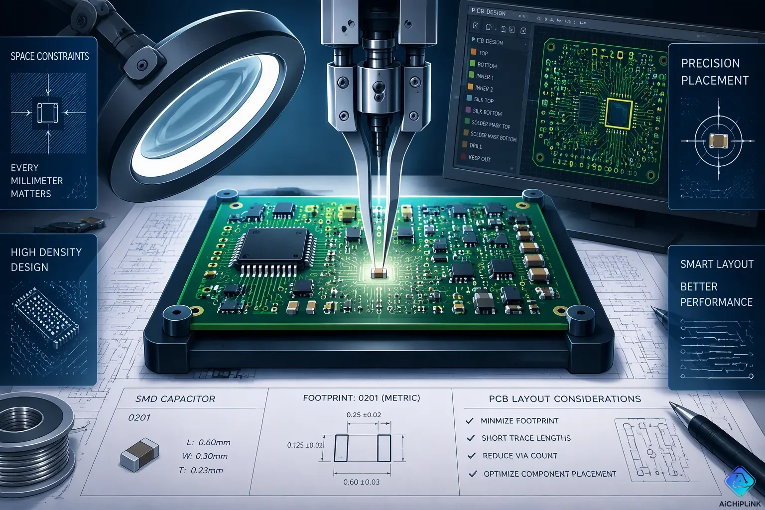
Having trouble fitting 1µF capacitance into your tight PCB layout? The TCC0402X6S105K100AT fixes this issue directly. This small capacitor provides 1µF in a tiny 0402 size with a 10V rating and X6S dielectric. Moving from a standard 0805 package to this 0402 part cuts board area by about 80%. You save valuable space without losing performance.
This part removes the need to choose between size and power for low-voltage circuits. You can safely run 3.3V or 5V power lines. The X6S dielectric keeps capacitance steady when temperature changes. Your mechanical design gets easier, and stress on the board drops. You get more routing paths and lower component height. For tight PCB layouts, this capacitor gives a practical, dependable answer that keeps your design small and your circuits working well.
Key Takeaways
-
Switching to the 0402 package uses 80% less board space per capacitor than an 0805 part.
-
One 1µF 0402 capacitor gives better decoupling than two 100nF capacitors and also cuts down the number of parts.
-
The X6S dielectric keeps its capacitance steady from -55°C to +105°C, making sure it works well in many different temperatures.
-
Put the capacitor 1-2mm from the IC power pins, and use even pads to stop soldering problems.
The PCB Space Crisis
Why Every Square Millimeter Counts
Modern electronics need incredible density. You pack more features into smaller cases every year. Smartphones, wearables, and IoT sensors all push this trend. Each part you place uses up precious board space. Each trace you route needs room around it. The result? You battle for every tiny bit of your PCB.
Your design choices affect the whole product. A smaller board means a thinner device. A thinner device means less weight and lower material costs. You also gain more design freedom. You can fit your product into tighter cases. You can add more features without making the housing bigger. These mechanical benefits lead directly to better market position.
The pressure grows with each design update. You add new functions, new sensors, new ways to connect. Every addition needs more board space. Yet your case size rarely gets bigger. You must find smart ways to win back space. This reality guides every choice you make during PCB design.
Traditional Capacitors as Space Bottlenecks
Capacitors often cause the biggest space problems. Decoupling capacitors sit near every IC power pin. Filtering capacitors appear throughout your power system. A typical design might use dozens of them. Each one takes up valuable space. Traditional packages waste this chance.
Look at the physical size of common capacitor packages. The table below shows the big differences:
| Package | Length (mm) | Width (mm) | Calculated Area (mm²) |
|---|---|---|---|
| 0402 | 1.0 | 0.5 | 0.5 |
| 0603 | 1.6 | 0.8 | 1.28 |
| 0805 | 2.0 | 1.25 | 2.5 |
These numbers tell a clear story. A 0603 capacitor takes up 2.56 times the board area of a 0402 part. An 0805 uses five times that space. When you need 1µF capacitance, older designs forced you into these bigger packages. You gave up precious area just to store the same energy.
This waste hurts your whole layout. Larger parts block routing paths. They create barriers for signal traces. They limit where you can place parts near dense ICs. Your PCB becomes harder to design. You face extra mechanical limits. Every oversized capacitor reduces your ability to improve the layout. The fix needs a basic change in how you pick components.
Introducing the tcc0402x6s105k100at: High Capacitance in an 0402 Package
The CCTC tcc0402x6s105k100at provides 1µF in a very small 0402 package. This surface-mount MLCC has a 10V rating and X6S dielectric. It offers ±10% tolerance and steady capacitance from -55°C to +105°C. CCTC builds this part with a nickel barrier termination for strong solder joints. AIChipLink, an AS9120 certified supplier, offers full traceability and quality checks. The part meets RoHS environmental rules. These specs make it a great pick for tight designs.
Why the 0402 Package and 1µF Capacitance Matter for Space-Constrained Designs
The 0402 package size gives you a key edge in crowded pcb layouts. Smaller packages like this one have lower Equivalent Series Inductance (ESL). Lower ESL means better high-frequency decoupling performance. You can put the capacitor closer to the IC power pins. This close placement is a must for good decoupling in dense layouts. Your circuit stays clean and steady.
The 1µF capacitance value also counts. In the past, engineers used 100nF capacitors because 1µF parts were too big and had high parasitic inductance. Modern MLCC technology changes that. A single 1µF capacitor in an 0402 package gives much lower impedance across a wide frequency range. It beats the old 100nF parts, especially above 40MHz. Using one 1µF part instead of a 100nF plus a bulk capacitor saves board space. Your pcb design gets simpler and more efficient. You also cut assembly costs with fewer parts to place. This one-part approach removes the old big/little method completely.
The mechanical perks of this package are obvious. A smaller part lowers mechanical stress on the board. It reduces part height and opens routing paths. You get more room to place other parts near dense ICs. This benefit directly boosts your overall design.
The Role of X6S Dielectric and 10V Rating in Reliability
The X6S dielectric keeps capacitance stable across temperature. Capacitance shifts by only ±22% from -55°C to +105°C. This stability covers consumer and industrial settings. Your circuit works well whether the device is cold or hot. The ±10% tolerance gives you exact values for key functions.
The 10V rating needs careful voltage handling. Use this capacitor with 3.3V or 5V supply rails. Running at 5V gives you a 50% derating margin against the 10V max. This margin greatly boosts part reliability. A common industry rule says to derate ceramic capacitors by at least 50% for best reliability. The max rated voltage should be double the normal working voltage. A 10V capacitor at 5V meets this double rule perfectly.
Voltage is one of the strongest accelerators for a number of failure mechanisms in capacitors. Therefore, reducing the applied voltage significantly improves component reliability.
A 10V capacitor at 5V faces less electrical stress and lasts longer. The nickel barrier termination adds strength to the solder joint. For a 12V rail, you need a higher rated part like 25V. The 10V rating fits low-voltage circuits well. It works for 3.3V and 5V rails with strong reliability margins.
The X6S dielectric and 10V rating together form a dependable part. You get stable capacitance over temperature and voltage. Your pcb gains from a part that handles real-world conditions without failure. The nickel barrier termination supports long-term durability. You can trust this tcc0402x6s105k100at for your next design.
Footprint Comparison: 0402 vs. Larger Packages
Quantifying the Board Area Reduction
You need to see the real difference in numbers. The table below shows the physical dimensions of both packages:
| Package (Imperial) | Length (mm) | Width (mm) |
|---|---|---|
| 0805 | 2.00 | 1.25 |
| 0402 | 1.00 | 0.50 |
The math tells a clear story. An 0805 capacitor measures 2.00 mm by 1.25 mm. That gives you a footprint of 2.5 square millimeters. The 0402 package measures 1.00 mm by 0.50 mm. That gives you only 0.5 square millimeters. When you divide 0.5 by 2.5, you get 0.2. This means the 0402 part takes up only 20 percent of the area that an 0805 requires. You save 80 percent of the board space for each capacitor you replace.
Think about a typical design with twenty decoupling capacitors. If you switch all of them from 0805 to 0402, you reclaim 40 square millimeters of board area. That space becomes available for other components. You can add features without enlarging the board. You can shrink the overall product size. You can reduce material costs. Every square millimeter you save gives you more options.
The weight difference also matters. Smaller parts weigh less. This reduction helps in portable devices where every gram counts. Drones, wearables, and handheld instruments all benefit from lighter components. The mechanical load on the board decreases as well. Smaller parts create less stress during vibration and thermal cycling. Your assembly becomes more robust over time.
Simplifying Layout and Reducing Component Count
The tcc0402x6s105k100at also simplifies your pcb design in another way. You can replace multiple smaller capacitors with one 1µF part. Older designs often used two 100nF capacitors in parallel to achieve adequate decoupling. This approach consumed twice the board area. It also doubled the component count. Each additional part adds assembly time and potential failure points.
A single 1µF capacitor in the 0402 package delivers better performance than two 100nF parts. The larger capacitance value provides lower impedance across a wider frequency range. You get superior decoupling with fewer components. Your bill of materials becomes shorter. Your inventory management gets easier. Your assembly process becomes faster and more reliable.
This consolidation creates more routing channels on your board. With fewer components blocking the way, you can route traces more directly. Signal paths become shorter. Crosstalk between traces decreases. Your overall signal integrity improves without extra effort.
The mechanical benefits extend beyond weight. A smaller component footprint gives you more flexibility in placement. You can position the capacitor closer to the IC power pin. This short distance reduces parasitic inductance. Your decoupling performance improves because the capacitor responds faster to current demands.
Your pcb design workflow also becomes simpler. You spend less time wrestling with component placement. You have more freedom to optimize trace paths. You can achieve a cleaner layout with fewer compromises. The design process moves faster from concept to production.
The space savings compound across your entire board. Each capacitor you shrink frees up area for other functions. You might fit additional sensors, connectors, or test points. You might reduce the number of board layers needed. Fewer layers mean lower manufacturing costs. The savings multiply across high-volume production runs.
When you compare the tcc0402x6s105k100at against larger alternatives, the choice becomes obvious. You gain board area, reduce component count, improve electrical performance, and simplify your mechanical design. These advantages make the 0402 package the smart choice for space-constrained applications.
Performance Considerations for Low‑Voltage Circuits
Temperature Stability of the X6S Dielectric
The X6S dielectric keeps capacitance steady over a wide range of temperatures. Your capacitor changes by only ±22% from -55°C to +105°C. This covers most consumer and industrial settings. Your circuit works well whether the device is in a cold storage area or a warm server room.
Think about a typical use case. Your product runs at room temperature near 25°C. The capacitor gives its full 1µF value at that point. If the surrounding temperature goes up to 85°C, the capacitance stays within the ±22% limit. Your circuit keeps running without problems. The same is true for cold conditions down to -55°C. This stability means you need fewer extra parts to fix temperature changes. You keep your pcb layout simpler and more efficient.
The stable dielectric also helps your mechanical design. Fewer changes in performance due to heat mean less stress on nearby parts. Your circuit keeps steady timing and filtering. This reliability helps you pass environmental tests faster. You spend less time fixing temperature issues during development.
Capacitance vs. DC Bias Behavior at 10V
DC bias derating affects all ceramic capacitors. When you apply a DC voltage, the capacitance drops. This effect is strongest in high-capacitance MLCCs with Class 2 dielectrics. But the TCC0402X6S105K100AT has very little derating at its 10V rating.
Why does this matter for your circuit? Your design runs on 3.3V or 5V power lines. These voltages stay well below the 10V rating. At 5V, you use only 50% of the rated voltage. The capacitor loses very little capacitance under these conditions. You get close to the full 1µF value in practice. Your calculations are accurate without needing large safety margins.
This behavior makes your design process simpler. You do not need to overcompensate for DC bias losses. You can trust the capacitance value in the datasheet. The 10V rating covers common low-voltage rails with plenty of room. Your circuit keeps its intended performance under all operating conditions.
When you combine temperature stability and little DC bias derating, you get a reliable part for space-constrained designs. Your pcb benefits from predictable performance without surprises. The mechanical layout stays the same because the electrical behavior remains stable.
Practical Layout Tips for the 0402 Capacitor
Optimizing Pad Geometry for Reliable Solder Joints
Your pad shape directly controls solder joint quality. Start with IPC-7351B standard land patterns as your starting point. For an 0402 capacitor, typical pads are 0.5 mm by 0.6 mm with a 0.4 mm gap. Keep both pads the same size and shape. If one pad is 20 percent bigger, it warms up slower. That delay causes uneven soldering and can lead to tombstoning.
Heat balance matters beyond the pad shape. Trace routing and power planes change how each pad heats. Connect one pad with a thin trace and the other with a thick trace. The thicker trace works like a heat sink. It pulls heat away from the pad and creates imbalance. Putting a pad inside a power plane makes this issue worse. Balance the routing between both pads. Use thermal relief spokes when connecting to metal planes.
IPC-7351 guideline for 0402 resistor: Pads might be 0.5 mm x 0.6 mm with a 0.4 mm gap. Keep both pads the same size and shape; if one pad is 20% bigger, it warms up slower, delaying wetting. Check spacing to match the component's footprint exactly.
Place 0402 capacitors away from board edges. Board edges face clamping and bending during assembly. Small parts near edges get more mechanical stress. Keep them inside the board boundary. Make sure rows of small passives face the same direction. Directional heat changes cause uneven warming. Consistent direction lowers this risk.
Placement Strategies to Free Up Routing Channels
Put your decoupling capacitor within 1-2 mm of the IC power pins. This close distance lowers trace inductance. Your capacitor sends current faster when the IC needs it. For high-speed microcontrollers and FPGAs, this distance is critical. You stop voltage drops in the power delivery network.
Use micro-vias or buried vias to connect capacitor pads to inner layers. These small vias take less board space than standard vias. You open up routing channels on the surface layer. Signal traces move between components easily. Your pcb layout becomes simpler to handle.
The pcb design also gains from smart placement. Group your capacitors close to the ICs they support. This method shortens trace length and boosts performance. It opens routing space for other signals. You avoid long paths around scattered parts.
Think about the mechanical limits of your board design. Small capacitors in an 0402 package create less mechanical stress. You place them in tight spots without bending the board. This mechanical freedom helps you fit more functions into the same area.
Each capacitor placed near its IC frees up space elsewhere. Your pcb gains from simpler paths. You get more routing options for other traces. The final board becomes cleaner.
This capacitor solves your space problem without sacrificing reliability. You reclaim significant board area with the 0402 footprint. The 10V rating covers your 3.3V and 5V rails safely. The X6S dielectric maintains stable capacitance across temperature extremes. Your pcb design becomes simpler with fewer components and better routing options. You reduce mechanical stress and gain mechanical freedom in tight layouts. This design choice delivers dependable performance for low-voltage circuits. The smaller footprint also improves high-frequency decoupling. Next time you redesign a space-constrained pcb, specify the CCTC TCC0402X6S105K100AT from AIChipLink to reclaim valuable board real estate.

Written by Jack Elliott from AIChipLink.
AIChipLink, one of the fastest-growing global independent electronic components distributors in the world, offers millions of products from thousands of manufacturers, and many of our in-stock parts is available to ship same day.
We mainly source and distribute integrated circuit (IC) products of brands such as Broadcom, Microchip, Texas Instruments, Infineon, NXP, Analog Devices, Qualcomm, Intel, etc., which are widely used in communication & network, telecom, industrial control, new energy and automotive electronics.
Empowered by AI, Linked to the Future. Get started on AIChipLink and submit your RFQ online today!
Frequently Asked Questions
Can I replace my 0805 capacitor with this 0402 part directly?
Yes, you can make this swap when your circuit runs at 10V or less. The 0402 package saves about 80% board area for each capacitor. Your pcb layout gains plenty of free space. Check your solder paste stencil thickness first. Thinner stencils work better for small parts.
What voltage rails work best with this capacitor?
This capacitor fits 3.3V and 5V supply rails perfectly. A 10V rating gives you a 50% derating margin at 5V operation. This margin boosts long-term reliability. For 12V rails, pick a higher-rated part instead. Your design stays safe when you respect voltage limits.
How does the X6S dielectric perform in hot environments?
The X6S dielectric shifts capacitance by only ±22% from -55°C to +105°C. Your circuit keeps stable performance across this range. This stability lowers mechanical stress from thermal cycling. You avoid adding compensation components. Your design passes environmental tests without extra effort.
What pad layout prevents soldering defects?
Follow IPC-7351B land patterns for reliable joints. Keep both pads equal in size and shape. Balance trace widths connecting to each pad. Uneven heating causes tombstoning defects. Place the capacitor away from board edges. This placement reduces mechanical strain during assembly.
Does this small capacitor affect routing flexibility?
No, the 0402 footprint actually boosts your routing options. Smaller parts create fewer obstacles for signal traces. You gain more channels between components. Place the capacitor within 1-2mm of IC power pins. Use micro-vias to connect inner layers and free up surface space.